EP4170717A1 - Substrat matriciel et son procédé de fabrication - Google Patents
Substrat matriciel et son procédé de fabrication Download PDFInfo
- Publication number
- EP4170717A1 EP4170717A1 EP20942098.3A EP20942098A EP4170717A1 EP 4170717 A1 EP4170717 A1 EP 4170717A1 EP 20942098 A EP20942098 A EP 20942098A EP 4170717 A1 EP4170717 A1 EP 4170717A1
- Authority
- EP
- European Patent Office
- Prior art keywords
- disposed
- insulating layer
- layer
- gate
- gate insulating
- Prior art date
- Legal status (The legal status is an assumption and is not a legal conclusion. Google has not performed a legal analysis and makes no representation as to the accuracy of the status listed.)
- Pending
Links
Images

Classifications
-
- H—ELECTRICITY
- H10—SEMICONDUCTOR DEVICES; ELECTRIC SOLID-STATE DEVICES NOT OTHERWISE PROVIDED FOR
- H10D—INORGANIC ELECTRIC SEMICONDUCTOR DEVICES
- H10D30/00—Field-effect transistors [FET]
- H10D30/60—Insulated-gate field-effect transistors [IGFET]
- H10D30/67—Thin-film transistors [TFT]
- H10D30/6704—Thin-film transistors [TFT] having supplementary regions or layers in the thin films or in the insulated bulk substrates for controlling properties of the device
- H10D30/6723—Thin-film transistors [TFT] having supplementary regions or layers in the thin films or in the insulated bulk substrates for controlling properties of the device having light shields
-
- H—ELECTRICITY
- H10—SEMICONDUCTOR DEVICES; ELECTRIC SOLID-STATE DEVICES NOT OTHERWISE PROVIDED FOR
- H10D—INORGANIC ELECTRIC SEMICONDUCTOR DEVICES
- H10D86/00—Integrated devices formed in or on insulating or conducting substrates, e.g. formed in silicon-on-insulator [SOI] substrates or on stainless steel or glass substrates
- H10D86/01—Manufacture or treatment
- H10D86/021—Manufacture or treatment of multiple TFTs
-
- H—ELECTRICITY
- H10—SEMICONDUCTOR DEVICES; ELECTRIC SOLID-STATE DEVICES NOT OTHERWISE PROVIDED FOR
- H10D—INORGANIC ELECTRIC SEMICONDUCTOR DEVICES
- H10D86/00—Integrated devices formed in or on insulating or conducting substrates, e.g. formed in silicon-on-insulator [SOI] substrates or on stainless steel or glass substrates
- H10D86/01—Manufacture or treatment
- H10D86/021—Manufacture or treatment of multiple TFTs
- H10D86/0221—Manufacture or treatment of multiple TFTs comprising manufacture, treatment or patterning of TFT semiconductor bodies
-
- H—ELECTRICITY
- H10—SEMICONDUCTOR DEVICES; ELECTRIC SOLID-STATE DEVICES NOT OTHERWISE PROVIDED FOR
- H10D—INORGANIC ELECTRIC SEMICONDUCTOR DEVICES
- H10D86/00—Integrated devices formed in or on insulating or conducting substrates, e.g. formed in silicon-on-insulator [SOI] substrates or on stainless steel or glass substrates
- H10D86/01—Manufacture or treatment
- H10D86/021—Manufacture or treatment of multiple TFTs
- H10D86/0231—Manufacture or treatment of multiple TFTs using masks, e.g. half-tone masks
-
- H—ELECTRICITY
- H10—SEMICONDUCTOR DEVICES; ELECTRIC SOLID-STATE DEVICES NOT OTHERWISE PROVIDED FOR
- H10D—INORGANIC ELECTRIC SEMICONDUCTOR DEVICES
- H10D86/00—Integrated devices formed in or on insulating or conducting substrates, e.g. formed in silicon-on-insulator [SOI] substrates or on stainless steel or glass substrates
- H10D86/40—Integrated devices formed in or on insulating or conducting substrates, e.g. formed in silicon-on-insulator [SOI] substrates or on stainless steel or glass substrates characterised by multiple TFTs
-
- H—ELECTRICITY
- H10—SEMICONDUCTOR DEVICES; ELECTRIC SOLID-STATE DEVICES NOT OTHERWISE PROVIDED FOR
- H10D—INORGANIC ELECTRIC SEMICONDUCTOR DEVICES
- H10D86/00—Integrated devices formed in or on insulating or conducting substrates, e.g. formed in silicon-on-insulator [SOI] substrates or on stainless steel or glass substrates
- H10D86/40—Integrated devices formed in or on insulating or conducting substrates, e.g. formed in silicon-on-insulator [SOI] substrates or on stainless steel or glass substrates characterised by multiple TFTs
- H10D86/421—Integrated devices formed in or on insulating or conducting substrates, e.g. formed in silicon-on-insulator [SOI] substrates or on stainless steel or glass substrates characterised by multiple TFTs having a particular composition, shape or crystalline structure of the active layer
-
- H—ELECTRICITY
- H10—SEMICONDUCTOR DEVICES; ELECTRIC SOLID-STATE DEVICES NOT OTHERWISE PROVIDED FOR
- H10D—INORGANIC ELECTRIC SEMICONDUCTOR DEVICES
- H10D86/00—Integrated devices formed in or on insulating or conducting substrates, e.g. formed in silicon-on-insulator [SOI] substrates or on stainless steel or glass substrates
- H10D86/40—Integrated devices formed in or on insulating or conducting substrates, e.g. formed in silicon-on-insulator [SOI] substrates or on stainless steel or glass substrates characterised by multiple TFTs
- H10D86/421—Integrated devices formed in or on insulating or conducting substrates, e.g. formed in silicon-on-insulator [SOI] substrates or on stainless steel or glass substrates characterised by multiple TFTs having a particular composition, shape or crystalline structure of the active layer
- H10D86/423—Integrated devices formed in or on insulating or conducting substrates, e.g. formed in silicon-on-insulator [SOI] substrates or on stainless steel or glass substrates characterised by multiple TFTs having a particular composition, shape or crystalline structure of the active layer comprising semiconductor materials not belonging to the Group IV, e.g. InGaZnO
-
- H—ELECTRICITY
- H10—SEMICONDUCTOR DEVICES; ELECTRIC SOLID-STATE DEVICES NOT OTHERWISE PROVIDED FOR
- H10D—INORGANIC ELECTRIC SEMICONDUCTOR DEVICES
- H10D86/00—Integrated devices formed in or on insulating or conducting substrates, e.g. formed in silicon-on-insulator [SOI] substrates or on stainless steel or glass substrates
- H10D86/40—Integrated devices formed in or on insulating or conducting substrates, e.g. formed in silicon-on-insulator [SOI] substrates or on stainless steel or glass substrates characterised by multiple TFTs
- H10D86/441—Interconnections, e.g. scanning lines
-
- H—ELECTRICITY
- H10—SEMICONDUCTOR DEVICES; ELECTRIC SOLID-STATE DEVICES NOT OTHERWISE PROVIDED FOR
- H10D—INORGANIC ELECTRIC SEMICONDUCTOR DEVICES
- H10D86/00—Integrated devices formed in or on insulating or conducting substrates, e.g. formed in silicon-on-insulator [SOI] substrates or on stainless steel or glass substrates
- H10D86/40—Integrated devices formed in or on insulating or conducting substrates, e.g. formed in silicon-on-insulator [SOI] substrates or on stainless steel or glass substrates characterised by multiple TFTs
- H10D86/481—Integrated devices formed in or on insulating or conducting substrates, e.g. formed in silicon-on-insulator [SOI] substrates or on stainless steel or glass substrates characterised by multiple TFTs integrated with passive devices, e.g. auxiliary capacitors
-
- H—ELECTRICITY
- H10—SEMICONDUCTOR DEVICES; ELECTRIC SOLID-STATE DEVICES NOT OTHERWISE PROVIDED FOR
- H10D—INORGANIC ELECTRIC SEMICONDUCTOR DEVICES
- H10D86/00—Integrated devices formed in or on insulating or conducting substrates, e.g. formed in silicon-on-insulator [SOI] substrates or on stainless steel or glass substrates
- H10D86/40—Integrated devices formed in or on insulating or conducting substrates, e.g. formed in silicon-on-insulator [SOI] substrates or on stainless steel or glass substrates characterised by multiple TFTs
- H10D86/60—Integrated devices formed in or on insulating or conducting substrates, e.g. formed in silicon-on-insulator [SOI] substrates or on stainless steel or glass substrates characterised by multiple TFTs wherein the TFTs are in active matrices
-
- H—ELECTRICITY
- H10—SEMICONDUCTOR DEVICES; ELECTRIC SOLID-STATE DEVICES NOT OTHERWISE PROVIDED FOR
- H10K—ORGANIC ELECTRIC SOLID-STATE DEVICES
- H10K59/00—Integrated devices, or assemblies of multiple devices, comprising at least one organic light-emitting element covered by group H10K50/00
- H10K59/10—OLED displays
- H10K59/12—Active-matrix OLED [AMOLED] displays
-
- H—ELECTRICITY
- H10—SEMICONDUCTOR DEVICES; ELECTRIC SOLID-STATE DEVICES NOT OTHERWISE PROVIDED FOR
- H10K—ORGANIC ELECTRIC SOLID-STATE DEVICES
- H10K59/00—Integrated devices, or assemblies of multiple devices, comprising at least one organic light-emitting element covered by group H10K50/00
- H10K59/10—OLED displays
- H10K59/12—Active-matrix OLED [AMOLED] displays
- H10K59/121—Active-matrix OLED [AMOLED] displays characterised by the geometry or disposition of pixel elements
- H10K59/1213—Active-matrix OLED [AMOLED] displays characterised by the geometry or disposition of pixel elements the pixel elements being TFTs
-
- H—ELECTRICITY
- H10—SEMICONDUCTOR DEVICES; ELECTRIC SOLID-STATE DEVICES NOT OTHERWISE PROVIDED FOR
- H10K—ORGANIC ELECTRIC SOLID-STATE DEVICES
- H10K59/00—Integrated devices, or assemblies of multiple devices, comprising at least one organic light-emitting element covered by group H10K50/00
- H10K59/10—OLED displays
- H10K59/12—Active-matrix OLED [AMOLED] displays
- H10K59/121—Active-matrix OLED [AMOLED] displays characterised by the geometry or disposition of pixel elements
- H10K59/1216—Active-matrix OLED [AMOLED] displays characterised by the geometry or disposition of pixel elements the pixel elements being capacitors
Definitions
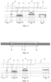
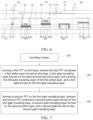
- the multifunctional metal layer further comprises a capacitor sublayer disposed on the substrate, a first capacitor electrode corresponding to the capacitor sublayer is disposed on the first gate insulating layer, an interlayer insulating layer covering the first gate insulating layer, the first gate, the second TFT, the signal line, and the first capacitor electrode is disposed on the first gate insulating layer, the first gate, the second TFT, the signal line, and the first capacitor electrode, and a second capacitor electrode corresponding to the first capacitor electrode is disposed on the interlayer insulating layer.
- first and second are used for describing purposes only, and cannot be understood as indicating or implying relative importance or implicitly indicating the number of technical features indicated.
- the features defined as “first” and “second” may explicitly or implicitly include one or more of the features.
- the meaning of “plurality” is two or more, unless it is specifically defined otherwise.
- the first gate of the first TFT and the second active layer of the second TFT are disposed in the same layer, are made of the same material, and use an integrally formed method.
- the first gate and the second active layer are formed through a photomask, while an insulating layer between the first gate and the second active layer is omitted, which can reduce the number of photomasks and processes.
- an inorganic insulating layer is further disposed on the interlayer insulating layer 41, the first source/drain 52, the second source/drain 62, and the second capacitor electrode 531 and covering the interlayer insulating layer 41, the first source/drain 52, the second source/drain 62, and the second capacitor electrode 531, then the inorganic insulating layer is disposed on the planarization layer 71, which is not limited herein.
- the first gate 23 and the second active layer 31 are made of a same material, and are integrally formed.
- the substrate may be glass.
- the substrate 11 may be a flexible material such as polyimide (PI).
- the substrate 11 comprises a flexible material such as PI and a barrier layer.
- the barrier layer may be an inorganic material, and an arrangement of the substrate 11 is not limited herein.
Landscapes
- Devices For Indicating Variable Information By Combining Individual Elements (AREA)
- Engineering & Computer Science (AREA)
- Microelectronics & Electronic Packaging (AREA)
- Electroluminescent Light Sources (AREA)
- Thin Film Transistor (AREA)
Applications Claiming Priority (2)
| Application Number | Priority Date | Filing Date | Title |
|---|---|---|---|
| CN202010580236.2A CN111755462B (zh) | 2020-06-23 | 2020-06-23 | 阵列基板及其制造方法 |
| PCT/CN2020/103098 WO2021258458A1 (fr) | 2020-06-23 | 2020-07-20 | Substrat matriciel et son procédé de fabrication |
Publications (2)
| Publication Number | Publication Date |
|---|---|
| EP4170717A1 true EP4170717A1 (fr) | 2023-04-26 |
| EP4170717A4 EP4170717A4 (fr) | 2024-08-07 |
Family
ID=79022300
Family Applications (1)
| Application Number | Title | Priority Date | Filing Date |
|---|---|---|---|
| EP20942098.3A Pending EP4170717A4 (fr) | 2020-06-23 | 2020-07-20 | Substrat matriciel et son procédé de fabrication |
Country Status (3)
| Country | Link |
|---|---|
| US (1) | US20210399024A1 (fr) |
| EP (1) | EP4170717A4 (fr) |
| JP (1) | JP7234380B2 (fr) |
Families Citing this family (6)
| Publication number | Priority date | Publication date | Assignee | Title |
|---|---|---|---|---|
| CN212033021U (zh) * | 2020-06-29 | 2020-11-27 | 京东方科技集团股份有限公司 | Tft基板及显示装置 |
| KR20230095445A (ko) * | 2021-12-22 | 2023-06-29 | 엘지디스플레이 주식회사 | 유기전계발광 표시장치 및 그 제조방법 |
| US12414368B2 (en) * | 2022-01-21 | 2025-09-09 | Wuhan China Star Optoelectronics | Display panel and method of manufacturing same |
| US20240397764A1 (en) * | 2022-02-25 | 2024-11-28 | Boe Technology Group Co., Ltd. | Display device and display panel |
| KR102852108B1 (ko) * | 2022-06-21 | 2025-08-27 | 엘지디스플레이 주식회사 | 표시 장치 및 그 제조 방법 |
| CN116249393A (zh) * | 2023-01-20 | 2023-06-09 | 京东方科技集团股份有限公司 | 显示背板及其制作方法和显示面板 |
Family Cites Families (8)
| Publication number | Priority date | Publication date | Assignee | Title |
|---|---|---|---|---|
| EP4447113A3 (fr) * | 2014-12-31 | 2025-01-08 | LG Display Co., Ltd. | Fond de panier d'affichage ayant de multiples types de transistors à couches minces |
| KR20250108751A (ko) | 2014-12-31 | 2025-07-15 | 엘지디스플레이 주식회사 | 다수의 타입들의 박막 트랜지스터들을 갖는 디스플레이 백플레인 |
| CN107403804B (zh) | 2016-05-17 | 2020-10-30 | 群创光电股份有限公司 | 显示设备 |
| KR102582394B1 (ko) | 2016-08-30 | 2023-09-26 | 삼성디스플레이 주식회사 | 반도체 장치 |
| KR102731378B1 (ko) | 2016-08-31 | 2024-11-15 | 엘지디스플레이 주식회사 | 멀티 타입의 박막 트랜지스터를 포함하는 유기 발광 표시 장치 및 유기 발광 표시 장치 제조 방법 |
| KR102583770B1 (ko) | 2016-09-12 | 2023-10-06 | 삼성디스플레이 주식회사 | 메모리 트랜지스터 및 이를 갖는 표시장치 |
| KR102620228B1 (ko) * | 2018-08-16 | 2024-01-02 | 삼성디스플레이 주식회사 | 표시 장치 |
| CN110211974B (zh) * | 2019-06-12 | 2022-05-24 | 厦门天马微电子有限公司 | 一种阵列基板、显示面板及阵列基板的制造方法 |
-
2020
- 2020-07-20 US US17/056,762 patent/US20210399024A1/en not_active Abandoned
- 2020-07-20 JP JP2021538805A patent/JP7234380B2/ja active Active
- 2020-07-20 EP EP20942098.3A patent/EP4170717A4/fr active Pending
Also Published As
| Publication number | Publication date |
|---|---|
| US20210399024A1 (en) | 2021-12-23 |
| JP7234380B2 (ja) | 2023-03-07 |
| JP2022543939A (ja) | 2022-10-17 |
| EP4170717A4 (fr) | 2024-08-07 |
Similar Documents
| Publication | Publication Date | Title |
|---|---|---|
| EP4170717A1 (fr) | Substrat matriciel et son procédé de fabrication | |
| US8999750B2 (en) | Semiconductor device | |
| CN101344695B (zh) | 显示面板及其制造方法 | |
| CN101044627B (zh) | 半导体器件 | |
| TWI606518B (zh) | 顯示裝置和其製造方法 | |
| US10622427B2 (en) | Array substrate, manufacturing method thereof, and display apparatus | |
| KR102089244B1 (ko) | 더블 게이트형 박막 트랜지스터 및 이를 포함하는 유기 발광 다이오드 표시장치 | |
| JP2012099824A (ja) | 電子機器 | |
| CN111755462B (zh) | 阵列基板及其制造方法 | |
| US20250031531A1 (en) | Display substrate and display device | |
| CN106409844A (zh) | 底栅型多晶硅tft基板及其制作方法 | |
| KR20160118122A (ko) | 디스플레이 패널 | |
| WO2016173012A1 (fr) | Substrat de matrice de transistors en couches et son procédé de fabrication | |
| CN109545836B (zh) | 一种oled显示装置及其制作方法 | |
| US20130100005A1 (en) | LCD Panel and Method of Manufacturing the Same | |
| KR101735833B1 (ko) | 유기전계발광표시장치 및 그 제조방법 | |
| CN113380863A (zh) | 显示面板及电子设备 | |
| US20260006850A1 (en) | Array substrate and display panel including the same | |
| KR20060090877A (ko) | 표시장치용 박막트랜지스터 기판과 그 제조방법 | |
| US20130106679A1 (en) | Lcd panel and method of manufacturing the same | |
| US11587917B2 (en) | Backlight module, display panel and electronic device | |
| US20250234647A1 (en) | Array substrate and display panel | |
| TWI411105B (zh) | 主動元件陣列基板、有機發光二極體顯示器裝置及其製造方法 | |
| KR20060125519A (ko) | 박막 트랜지스터 및 그 제조 방법과 액정 표시 장치 | |
| CN114695501A (zh) | 显示面板 |
Legal Events
| Date | Code | Title | Description |
|---|---|---|---|
| STAA | Information on the status of an ep patent application or granted ep patent |
Free format text: STATUS: THE INTERNATIONAL PUBLICATION HAS BEEN MADE |
|
| PUAI | Public reference made under article 153(3) epc to a published international application that has entered the european phase |
Free format text: ORIGINAL CODE: 0009012 |
|
| STAA | Information on the status of an ep patent application or granted ep patent |
Free format text: STATUS: REQUEST FOR EXAMINATION WAS MADE |
|
| 17P | Request for examination filed |
Effective date: 20220517 |
|
| AK | Designated contracting states |
Kind code of ref document: A1 Designated state(s): AL AT BE BG CH CY CZ DE DK EE ES FI FR GB GR HR HU IE IS IT LI LT LU LV MC MK MT NL NO PL PT RO RS SE SI SK SM TR |
|
| DAV | Request for validation of the european patent (deleted) | ||
| DAX | Request for extension of the european patent (deleted) | ||
| A4 | Supplementary search report drawn up and despatched |
Effective date: 20240705 |
|
| RIC1 | Information provided on ipc code assigned before grant |
Ipc: H01L 27/12 20060101AFI20240701BHEP |