EP4170821B1 - Rfic-zusammengesetzte antenne - Google Patents
Rfic-zusammengesetzte antenne Download PDFInfo
- Publication number
- EP4170821B1 EP4170821B1 EP22201951.5A EP22201951A EP4170821B1 EP 4170821 B1 EP4170821 B1 EP 4170821B1 EP 22201951 A EP22201951 A EP 22201951A EP 4170821 B1 EP4170821 B1 EP 4170821B1
- Authority
- EP
- European Patent Office
- Prior art keywords
- slot
- rfic
- pattern
- layer substrate
- present disclosure
- Prior art date
- Legal status (The legal status is an assumption and is not a legal conclusion. Google has not performed a legal analysis and makes no representation as to the accuracy of the status listed.)
- Active
Links
Images


Classifications
-
- H—ELECTRICITY
- H01—ELECTRIC ELEMENTS
- H01Q—ANTENNAS, i.e. RADIO AERIALS
- H01Q19/00—Combinations of primary active antenna elements and units with secondary devices, e.g. with quasi-optical devices, for giving the antenna a desired directional characteristic
- H01Q19/28—Combinations of primary active antenna elements and units with secondary devices, e.g. with quasi-optical devices, for giving the antenna a desired directional characteristic using a secondary device in the form of two or more substantially straight conductive elements
- H01Q19/30—Combinations of primary active antenna elements and units with secondary devices, e.g. with quasi-optical devices, for giving the antenna a desired directional characteristic using a secondary device in the form of two or more substantially straight conductive elements the primary active element being centre-fed and substantially straight, e.g. Yagi antenna
-
- G—PHYSICS
- G06—COMPUTING OR CALCULATING; COUNTING
- G06K—GRAPHICAL DATA READING; PRESENTATION OF DATA; RECORD CARRIERS; HANDLING RECORD CARRIERS
- G06K19/00—Record carriers for use with machines and with at least a part designed to carry digital markings
- G06K19/06—Record carriers for use with machines and with at least a part designed to carry digital markings characterised by the kind of the digital marking, e.g. shape, nature, code
- G06K19/067—Record carriers with conductive marks, printed circuits or semiconductor circuit elements, e.g. credit or identity cards also with resonating or responding marks without active components
- G06K19/07—Record carriers with conductive marks, printed circuits or semiconductor circuit elements, e.g. credit or identity cards also with resonating or responding marks without active components with integrated circuit chips
- G06K19/077—Constructional details, e.g. mounting of circuits in the carrier
- G06K19/07749—Constructional details, e.g. mounting of circuits in the carrier the record carrier being capable of non-contact communication, e.g. constructional details of the antenna of a non-contact smart card
- G06K19/0775—Constructional details, e.g. mounting of circuits in the carrier the record carrier being capable of non-contact communication, e.g. constructional details of the antenna of a non-contact smart card arrangements for connecting the integrated circuit to the antenna
-
- H—ELECTRICITY
- H01—ELECTRIC ELEMENTS
- H01Q—ANTENNAS, i.e. RADIO AERIALS
- H01Q1/00—Details of, or arrangements associated with, antennas
- H01Q1/12—Supports; Mounting means
- H01Q1/22—Supports; Mounting means by structural association with other equipment or articles
- H01Q1/2283—Supports; Mounting means by structural association with other equipment or articles mounted in or on the surface of a semiconductor substrate as a chip-type antenna or integrated with other components into an IC package
-
- H—ELECTRICITY
- H01—ELECTRIC ELEMENTS
- H01Q—ANTENNAS, i.e. RADIO AERIALS
- H01Q1/00—Details of, or arrangements associated with, antennas
- H01Q1/36—Structural form of radiating elements, e.g. cone, spiral, umbrella; Particular materials used therewith
- H01Q1/38—Structural form of radiating elements, e.g. cone, spiral, umbrella; Particular materials used therewith formed by a conductive layer on an insulating support
-
- H—ELECTRICITY
- H01—ELECTRIC ELEMENTS
- H01Q—ANTENNAS, i.e. RADIO AERIALS
- H01Q1/00—Details of, or arrangements associated with, antennas
- H01Q1/52—Means for reducing coupling between antennas; Means for reducing coupling between an antenna and another structure
- H01Q1/526—Electromagnetic shields
-
- H—ELECTRICITY
- H01—ELECTRIC ELEMENTS
- H01Q—ANTENNAS, i.e. RADIO AERIALS
- H01Q23/00—Antennas with active circuits or circuit elements integrated within them or attached to them
-
- H—ELECTRICITY
- H01—ELECTRIC ELEMENTS
- H01Q—ANTENNAS, i.e. RADIO AERIALS
- H01Q3/00—Arrangements for changing or varying the orientation or the shape of the directional pattern of the waves radiated from an antenna or antenna system
- H01Q3/26—Arrangements for changing or varying the orientation or the shape of the directional pattern of the waves radiated from an antenna or antenna system varying the relative phase or relative amplitude of energisation between two or more active radiating elements; varying the distribution of energy across a radiating aperture
- H01Q3/267—Phased-array testing or checking devices
-
- H—ELECTRICITY
- H01—ELECTRIC ELEMENTS
- H01Q—ANTENNAS, i.e. RADIO AERIALS
- H01Q9/00—Electrically-short antennas having dimensions not more than twice the operating wavelength and consisting of conductive active radiating elements
- H01Q9/04—Resonant antennas
- H01Q9/16—Resonant antennas with feed intermediate between the extremities of the antenna, e.g. centre-fed dipole
- H01Q9/28—Conical, cylindrical, cage, strip, gauze, or like elements having an extended radiating surface; Elements comprising two conical surfaces having collinear axes and adjacent apices and fed by two-conductor transmission lines
- H01Q9/285—Planar dipole
Definitions
- the present disclosure relates to an antenna, and more particularly to an RFICz assembled antenna.
- 5G communication has been started, in which 5G performs communication using a millimeter wave band of 20 GHz or more compared to the existing 4G communication.
- the millimeter wave band has a very large attenuation characteristic compared to the low frequency band, and the signal loss due to an obstacle is very large.
- a conventional millimeter wave band antenna for a terminal was connected to a board of the terminal through a connector, and received a feed signal from an RFIC chip mounted on the board of the terminal.
- the millimeter wave band antenna has a small size
- a connector with fine precision was also required for the connector, and sophisticated work was also required to combine the millimeter wave band antenna with the connector.
- the connector due to the use of the connector, there was a problem that not only the size of the entire terminal increases, but also the manufacturing cost increases.
- US 9 806 422 B2 package structures are provided having antenna-in-packages that are integrated with semiconductor RFIC (radio frequency integrated circuit) chips to form compact integrated radio/wireless communications systems that operate in the millimeter wave (mmWave) frequency range with radiation in broadside and end-fire directions.
- RFIC radio frequency integrated circuit
- a dipole antenna element is provided at the back of a dielectric substrate set to the reflector surface.
- a parasitic element is provided on the front of the dielectric substrate, which is constituted by forming and protruding the central portion of a linear conductor forward in an almost trapezoidal shape, for example.
- An object of the present disclosure is to propose a millimeter wave band antenna having a structure in which an RFIC chip is assembled without being connected to an RFIC chip through a connector.
- Another object of the present disclosure is to propose a millimeter wave band antenna capable of reducing the size of a terminal and reducing manufacturing cost.
- Yet another object of the present disclosure is to propose a millimeter wave band antenna capable of forming a required radiation pattern while effectively blocking harmful electromagnetic waves.
- an RFIC assembled antenna comprising: a first layer substrate including a first metal pattern, a first slot formed in the first metal pattern, and a second slot formed in the first metal an RFIC chip which is coupled to a region of the second slot for assembling the RFIC chip with the first layer substrate; and a second layer substrate coupled to a lower portion of the first layer substrate and including a second metal pattern, a third slot formed in the second metal pattern, and a dipole radiator formed inside the third slot, wherein a feeding pattern connected to the RFIC chip to provide a feed signal to the dipole radiator is formed inside the first slot wherein the second slot is connected to the first slot.
- At least one parasitic pattern spaced apart from the feeding pattern by a predetermined distance and extending in a direction perpendicular to the longitudinal direction of the feeding pattern is formed inside the first slot.
- An auxiliary radiator spaced apart from the feeding pattern by a predetermined distance and extending in a direction parallel to the longitudinal direction of the feeding pattern is further formed inside the first slot, and the auxiliary radiator is connected to the RFIC chip.
- the auxiliary radiator receives a portion of the signal radiated from the dipole radiator and provides it to the RFIC chip.
- the antenna further includes a third layer substrate positioned below the second layer substrate, and at least one reflector is formed on the third layer substrate in a region that vertically overlaps with the first slot and the second slot.
- the antenna is coupled to an SMT region of a terminal board, and at least one via hole for providing a feed signal from the terminal board to the RFIC chip is formed in the first to third layer substrates.
- an RFIC assembled antenna comprising: a first layer substrate including a first metal pattern, a first slot formed in the first metal pattern, and a second slot formed to be connected to the first slot, and in which an RFIC chip is coupled to a region of the second slot; and a second layer substrate coupled to a lower portion of the first layer substrate and including a second metal pattern and a dipole radiator coupled to the second metal pattern, wherein a feeding pattern connected to the RFIC chip to provide a feed signal to the dipole radiator is formed inside the first slot or the second slot, and wherein a shield can for shielding the RFIC chip is coupled to a region of the second slot of the first layer substrate.
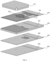
- FIG. 1 is an exploded perspective view showing a structure of an RFIC assembled antenna according to an embodiment of the present disclosure
- FIG. 2 is a plan view of a first layer substrate in an RFIC assembled antenna according to an embodiment of the present disclosure
- FIG. 3 is a plan view of a second layer substrate in an RFIC assembled antenna according to an embodiment of the present disclosure
- FIG. 4 is a plan view of a third layer substrate
- FIG. 5 is a plan view of a fourth layer substrate according to an embodiment of the present disclosure.
- the RFIC assembled antenna may include first to fourth layer substrates 100, 200, 300 and 400.
- the multi-layer structure for the RFIC assembled antenna of the present disclosure may be implemented using a multi-layer PCB.
- FIG. 1 illustrates a case composed of four layer substrates, it will be apparent to those skilled in the art that additional substrates may be provided to control the separation distance between respective substrates and to control the characteristics. In addition, it will also be apparent to those skilled in the art that certain layer substrates may be omitted.
- a first metal pattern 110 is formed on the first layer substrate 100.
- the first metal pattern 110 may have a ground potential.
- a first slot 120 and a second slot 130 are formed in the first metal pattern 110.
- the first slot 120 and the second slot 130 are formed by removing a portion of the metal region of the first metal pattern 110.
- the feeding pattern 140 is connected to the RFIC chip in the region of the second slot 130, and receives a feed signal from the RFIC chip.
- the feeding pattern 140 functions to provide a feed signal to the dipole radiator 230 formed on the second layer substrate 200 in a coupling manner.
- a ' '-shaped feeding pattern 140 is shown, but the shape of the feeding pattern 140 may be changed as needed.
- the first parasitic pattern 160 formed in the first slot 120 or the second slot 130 may be formed in a direction perpendicular to the longitudinal direction of the feeding pattern 140.
- the first parasitic pattern 160 is not electrically connected to the ground or signal line, and the first parasitic pattern 160 is formed to improve the gain of the radiation pattern of the dipole radiator 230 formed on the second layer substrate 200.
- the length of the first parasitic pattern 160 may be determined based on a used frequency and a required radiation pattern.
- a second parasitic pattern 170 and a third parasitic pattern 180 may be additionally formed in the first slot 120.
- the second parasitic pattern 170 and the third parasitic pattern 180 may be spaced apart from the first parasitic pattern 160, and formed in a direction parallel to the first parasitic pattern 160.
- the second parasitic pattern 170 and the third parasitic pattern 180 are also not electrically connected to the ground or the signal line.
- the second parasitic pattern 170 is spaced apart from the first parasitic pattern 160
- the third parasitic pattern 180 is spaced apart from the second parasitic pattern 170
- the third parasitic pattern 180 is disposed to be spaced apart from the first parasitic pattern by a greater distance compared to the second parasitic pattern 170.
- the third parasitic pattern 180 may be disposed adjacent to the edge region of the first slot.
- the second parasitic pattern 170 and the third parasitic pattern 180 also function to improve the gain of the radiation pattern.
- the auxiliary radiator 150 is electrically connected to the RFIC chip, and receives a portion of a signal radiated from the dipole radiator 230.
- the auxiliary radiator 150 receives a portion of a signal radiated from the dipole radiator 230.
- the auxiliary radiator 150 is used for determining whether a signal radiated from the dipole radiator 230 is appropriate, and receives a portion of the radiation signal.
- the signal received from the auxiliary radiator 150 is provided to the RFIC chip, and it is possible to determine whether the antenna malfunctions by analyzing the signal provided to the RFIC chip through the auxiliary radiator 150.
- a second slot 130 connected to the first slot 120 is formed in the first metal pattern 110 of the first layer substrate 100.
- the second slot 130 is a slot for placing an RFIC chip.
- a shield can may be disposed to shield the RFIC chip, and the shield can is also disposed in the region of the second slot 130.
- the second slot 130 is connected to the first slot 120, the width and shape are different from those of the first slot 120.
- a third metal pattern 190 is formed spaced apart from the first metal pattern 110, and a plurality of first via holes 195 are formed in the third metal pattern 190.
- the plurality of first via holes 195 may be formed in the longitudinal direction of the third metal pattern 190, and the plurality of first via holes 195 may be arranged to form two rows.
- the arrangement of the plurality of first via holes 195 illustrated in FIG. 1 is exemplary, and the plurality of first via holes 195 may be arranged in various ways.
- the radiation pattern of the antenna may be affected. Although the radiation pattern should be formed in a direction passing through the first slot and the second slot, the radiation pattern may be tilted due to the influence of the RFIC chip and the shield can.
- a third metal pattern 190 spaced apart from the first metal pattern is formed, and a plurality of first via holes 195 are formed in the third metal pattern 190.
- Via holes connected to the third metal pattern 190 are also formed in the second layer substrate 200, the third layer substrate 300 and the fourth layer substrate 400.
- a plurality of second via holes 295 connected to the first via holes 195 are formed in the second layer substrate 200
- a plurality of third via holes 395 connected to the plurality of second via holes 295 are formed in the third layer substrate 300
- a plurality of fourth via holes 495 connected to the plurality of third via holes 395 are formed in the fourth layer substrate 400.
- a conductive wall may be formed by forming via holes connected to each other in the first layer substrate 100 to the fourth layer substrate 400, and distortion of the radiation pattern can be prevented through the conductive wall.
- a second metal pattern 210 is formed on the second layer substrate 200.
- the second metal pattern 210 may have a ground potential.
- a dipole radiator 230 coupled to the second metal pattern 210 is formed on the second layer substrate 200.
- the dipole radiator 230 receives a feed signal from the feeding pattern 140 in a coupling manner.
- the dipole radiator 230 radiates the feed signal provided from the feeding pattern 140 to the outside.
- the dipole radiator 230 includes a first dipole arm 230-1 and a second dipole arm 230-2.
- the first dipole arm 230-1 and the second dipole arm 230-2 are spaced apart from each other.
- FIG. 3 a case is shown in which a dipole radiator 230 is used as the antenna radiator of the present disclosure, but it will be apparent to those skilled in the art that other types of radiator may be formed.
- reflectors 410 and 412 are formed on the third layer substrate 300.
- the reflectors 410 and 412 are preferably formed in a region overlapping the first slot 120 and the second slot 130 vertically. In FIG. 4 , a case is shown in which the two reflectors 410 and 412 are spaced apart from each other, but it will be apparent to those skilled in the art that a single reflector may be substituted.
- the reflectors 410 and 412 reflect the signals radiated in the downward direction among the radiation signals of the dipole radiator 230 to increase the gain in the upward direction of the radiation signals of the dipole radiator 230.
- the fourth layer substrate 400 is coupled to the lower portion of the third layer substrate 300.
- a ground plane (not shown) may be formed on a lower surface of the fourth layer substrate 400.
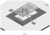
- FIG. 6 is an exploded perspective view of a state in which an RFIC is coupled in an antenna according to an embodiment of the present disclosure
- FIG. 7 is a plan view of a first layer substrate to which an RFIC is coupled.
- an RFIC chip 700 is coupled to the region of the second slot 130 of the antenna according to an embodiment of the present disclosure, and a shield can 710 for shielding the RFIC chip is coupled.
- the shield can 710 may not be coupled as needed.
- the RFIC chip 700 provides a feed signal to the feeding pattern 140, and the feeding pattern 140 is electrically connected to the RFIC chip 700.
- the RFIC chip 700 is electrically connected to the auxiliary radiator 150 to receive a signal received from the auxiliary radiator 150.
- the present disclosure proposes an antenna structure in which an RFIC chip is assembled without using a separate connector, by laminating the first layer substrate 100 on the second layer substrate 200 on which the dipole radiator 230 is formed, forming the first metal pattern 110 in which the first slot 120 and the second slot 130 are formed, and then coupling the RFIC chip on the first metal pattern 110.
- the RFIC chip 700 receives a feed signal from the PCB of the terminal, and via holes are formed in each layer substrate of the present disclosure to receive the feed signal from the PCB.
- FIGS. 6 and 7 an example is shown in which two via holes are formed on the left side and two via holes on the right side with respect to the RFIC chip.
- a shield can 710 for shielding the RFIC chip 700 may be additionally coupled.
- the shield can 710 is made of a conductive material, it may block unnecessary electromagnetic waves generated from the RFIC chip 700, but may distort the radiation pattern of the dipole radiator 230.
- a conductive wall is formed through the via holes 195, 295, 395 and 495 of each layer substrate.
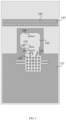
- FIG. 8 shows an example in which an RFIC assembled antenna according to an embodiment of the present disclosure is coupled on a substrate.
- an SMT region is set on the substrate, and the antenna made of the multi-layer substrate of the present disclosure is coupled to the SMT region. Since the antenna of the present disclosure has a structure in which the RFIC chip is assembled, it can be directly coupled to the substrate without being coupled to the substrate through a separate connector.
- via holes are formed in the antenna of the present disclosure so that a feed signal from the substrate is provided to the RFIC chip.
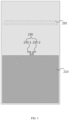
- FIG. 9 shows an example of a radiation pattern of an RFIC assembled antenna according to an embodiment of the present disclosure.
- a radiation pattern is formed in an upward direction of the antenna.
- the gain of the beam in the upward direction can be improved due to the first slot 120, the second slot 130 and the plurality of via holes.
- the reflectors 410 and 412 formed on the third layer substrate 300 may also contribute to the improvement of the gain of the beam, and the conductive wall formed through the plurality of via holes 195, 295, 395 and 495 may prevent the radiation pattern from being tilted.
- the auxiliary radiator 150 is located on the first layer substrate 100 that is an upper portion of the dipole radiator 230, it is possible to receive a portion of the signal radiated from the dipole radiator 230 to confirm whether an appropriate signal is radiated in an appropriate direction.
Landscapes
- Engineering & Computer Science (AREA)
- Microelectronics & Electronic Packaging (AREA)
- Physics & Mathematics (AREA)
- Computer Hardware Design (AREA)
- General Physics & Mathematics (AREA)
- Theoretical Computer Science (AREA)
- Electromagnetism (AREA)
- Aerials With Secondary Devices (AREA)
- Variable-Direction Aerials And Aerial Arrays (AREA)
Claims (6)
- RFIC-montierte Antenne, die Folgendes umfasst:ein erstes Schichtsubstrat (100), das ein erstes Metallmuster (110), eine in dem ersten Metallmuster (110) gebildete erste Aussparung (120) und eine in dem ersten Metallmuster (110) gebildete zweite Aussparung (130) enthält;einen RFIC-Chip (700), der mit einer Region der zweiten Aussparung (130) zum Montieren des RFIC-Chips (700) an dem ersten Schichtsubstrat (100) gekoppelt ist; undein zweites Schichtsubstrat (200), das mit einem unteren Abschnitt des ersten Schichtsubstrats (100) gekoppelt ist und ein zweites Metallmuster (210), eine in dem zweiten Metallmuster (210) gebildete dritte Aussparung und einen innerhalb der dritten Aussparung gebildeten Dipolstrahler (230) enthält,wobei innerhalb der ersten Aussparung (120) ein mit dem RFIC-Chip (700) verbundenes Einspeisungsmuster (140) zum Bereitstellen eines Einspeisungssignals für den Dipolstrahler (230) gebildet ist,wobei die zweite Aussparung (130) mit der ersten Aussparung (120) verbunden ist.
- RFIC-montierte Antenne nach Anspruch 1,
wobei innerhalb der ersten Aussparung (120) mindestens ein parasitäres Muster (160, 170, 180), das von dem Einspeisungsmuster (140) um einen vorgegebenen Abstand beabstandet ist und in einer zu einer Längsrichtung des Einspeisungsmusters (140) senkrechten Richtung verläuft, gebildet ist. - RFIC-montierte Antenne nach Anspruch 1 oder 2,
wobei innerhalb der ersten Aussparung (120) ferner ein Hilfsstrahler (150), der von dem Einspeisungsmuster (140) um einen vorgegebenen Abstand beabstandet ist und in einer zu der Längsrichtung des Einspeisungsmusters (140) parallelen Richtung verläuft, gebildet ist und der Hilfsstrahler (150) mit dem RFIC-Chip (700) verbunden ist. - RFIC-montierte Antenne nach den Ansprüchen 1 bis 3,
wobei der Hilfsstrahler (150) ein Stück des von dem Dipolstrahler (230) ausgesendeten Signals empfängt und es für den RFIC-Chip (700) bereitstellt. - RFIC-montierte Antenne nach den Ansprüchen 1 bis 4,die ferner ein drittes Schichtsubstrat (300), das unter dem zweiten Schichtsubstrat (200) positioniert ist, enthält,wobei auf dem dritten Schichtsubstrat (300) in einer Region, die mit der ersten Aussparung (120) und der zweiten Aussparung (130) vertikal überlappt, mindestens ein Reflektor (410, 412) gebildet ist.
- RFIC-montierte Antenne nach den Ansprüchen 1 bis 5,
wobei die Antenne mit einer SMT-Region einer Anschlussplatte gekoppelt ist und in dem ersten bis zu dem dritten Schichtsubstrat (300) mindestens ein Verbindungsloch (195, 295, 395, 495) zum Bereitstellen eines Einspeisungssignals von der Anschlussplatte für den RFIC-Chip (700) gebildet ist.
Applications Claiming Priority (2)
| Application Number | Priority Date | Filing Date | Title |
|---|---|---|---|
| KR1020210141695A KR102549577B1 (ko) | 2021-10-22 | 2021-10-22 | Rfic 일체형 안테나 |
| KR1020220012395A KR102571790B1 (ko) | 2022-01-27 | 2022-01-27 | Rfic 일체형 안테나 |
Publications (2)
| Publication Number | Publication Date |
|---|---|
| EP4170821A1 EP4170821A1 (de) | 2023-04-26 |
| EP4170821B1 true EP4170821B1 (de) | 2024-09-25 |
Family
ID=83898464
Family Applications (1)
| Application Number | Title | Priority Date | Filing Date |
|---|---|---|---|
| EP22201951.5A Active EP4170821B1 (de) | 2021-10-22 | 2022-10-17 | Rfic-zusammengesetzte antenne |
Country Status (2)
| Country | Link |
|---|---|
| US (1) | US12074360B2 (de) |
| EP (1) | EP4170821B1 (de) |
Family Cites Families (11)
| Publication number | Priority date | Publication date | Assignee | Title |
|---|---|---|---|---|
| JP3085524B2 (ja) | 1996-11-18 | 2000-09-11 | 日本電業工作株式会社 | 反射板付ダイポ−ルアンテナ |
| KR100917847B1 (ko) | 2006-12-05 | 2009-09-18 | 한국전자통신연구원 | 전방향 복사패턴을 갖는 평면형 안테나 |
| US9806422B2 (en) * | 2013-09-11 | 2017-10-31 | International Business Machines Corporation | Antenna-in-package structures with broadside and end-fire radiations |
| US9391370B2 (en) | 2014-06-30 | 2016-07-12 | Samsung Electronics Co., Ltd. | Antenna feed integrated on multi-layer PCB |
| KR102425821B1 (ko) | 2017-11-28 | 2022-07-27 | 삼성전자주식회사 | 커플링 급전을 이용한 이중 대역 안테나 및 그것을 포함하는 전자 장치 |
| KR102246620B1 (ko) | 2019-03-20 | 2021-05-03 | 삼성전기주식회사 | 안테나 장치 |
| KR102593888B1 (ko) * | 2019-06-13 | 2023-10-24 | 삼성전기주식회사 | 안테나 모듈 및 이를 포함하는 전자기기 |
| KR102733019B1 (ko) | 2019-07-17 | 2024-11-21 | 삼성전자주식회사 | 안테나 모듈 및 그것을 포함하는 전자 장치 |
| WO2021085669A1 (ko) * | 2019-10-30 | 2021-05-06 | 엘지전자 주식회사 | 5g 안테나를 구비하는 전자 기기 |
| EP4044366B1 (de) * | 2021-02-12 | 2023-10-25 | Sivers Wireless AB | Integrierte schaltungspackung mit gekreuzter dipolantenne |
| US20230014567A1 (en) * | 2021-07-14 | 2023-01-19 | Qualcomm Incorporated | Package substrate employing integrated slot-shaped antenna(s), and related integrated circuit (ic) packages and fabrication methods |
-
2022
- 2022-10-17 EP EP22201951.5A patent/EP4170821B1/de active Active
- 2022-10-17 US US18/047,089 patent/US12074360B2/en active Active
Also Published As
| Publication number | Publication date |
|---|---|
| US12074360B2 (en) | 2024-08-27 |
| US20230129616A1 (en) | 2023-04-27 |
| EP4170821A1 (de) | 2023-04-26 |
Similar Documents
| Publication | Publication Date | Title |
|---|---|---|
| US10944181B2 (en) | Antenna module and communication device | |
| JP6930591B2 (ja) | アンテナモジュールおよび通信装置 | |
| US9698487B2 (en) | Array antenna | |
| JP6195080B2 (ja) | アンテナ装置 | |
| US11456526B2 (en) | Antenna unit, antenna system and electronic device | |
| US7109948B2 (en) | Dielectric antenna module | |
| US11831085B2 (en) | Compact antenna radiating element | |
| CN110098480B (zh) | 片式天线及包括该片式天线的天线模块 | |
| KR102360974B1 (ko) | 엔드파이어 방사 패턴을 가지는 밀리미터 웨이브 대역 안테나 | |
| KR101901101B1 (ko) | 인쇄형 다이폴 안테나 및 이를 이용한 전자기기 | |
| KR20200008716A (ko) | 칩 안테나 모듈 | |
| WO2024120287A1 (zh) | 一种天线结构和电子设备 | |
| US12224490B2 (en) | Horn antenna for millimeter wave | |
| KR102571790B1 (ko) | Rfic 일체형 안테나 | |
| KR102370147B1 (ko) | Pcb 급전을 이용한 혼 안테나 | |
| EP4170821B1 (de) | Rfic-zusammengesetzte antenne | |
| US11217887B2 (en) | Antenna module | |
| CN115053404A (zh) | 天线装置以及通信装置 | |
| KR102549577B1 (ko) | Rfic 일체형 안테나 | |
| KR102624142B1 (ko) | Rfic 일체형 안테나 | |
| JP7852743B2 (ja) | アンテナモジュールおよびそれを搭載した通信装置 | |
| EP4554000A1 (de) | Antennenmodul | |
| US20240012135A1 (en) | Image radar apparatus with vertical feeding structure using waveguides | |
| WO2025123142A1 (en) | Integrated antenna array with feed and calibration networks | |
| WO2024114283A1 (zh) | 一种天线结构和电子设备 |
Legal Events
| Date | Code | Title | Description |
|---|---|---|---|
| PUAI | Public reference made under article 153(3) epc to a published international application that has entered the european phase |
Free format text: ORIGINAL CODE: 0009012 |
|
| STAA | Information on the status of an ep patent application or granted ep patent |
Free format text: STATUS: THE APPLICATION HAS BEEN PUBLISHED |
|
| AK | Designated contracting states |
Kind code of ref document: A1 Designated state(s): AL AT BE BG CH CY CZ DE DK EE ES FI FR GB GR HR HU IE IS IT LI LT LU LV MC ME MK MT NL NO PL PT RO RS SE SI SK SM TR |
|
| STAA | Information on the status of an ep patent application or granted ep patent |
Free format text: STATUS: REQUEST FOR EXAMINATION WAS MADE |
|
| 17P | Request for examination filed |
Effective date: 20231020 |
|
| RBV | Designated contracting states (corrected) |
Designated state(s): AL AT BE BG CH CY CZ DE DK EE ES FI FR GB GR HR HU IE IS IT LI LT LU LV MC ME MK MT NL NO PL PT RO RS SE SI SK SM TR |
|
| GRAP | Despatch of communication of intention to grant a patent |
Free format text: ORIGINAL CODE: EPIDOSNIGR1 |
|
| STAA | Information on the status of an ep patent application or granted ep patent |
Free format text: STATUS: GRANT OF PATENT IS INTENDED |
|
| INTG | Intention to grant announced |
Effective date: 20240422 |
|
| GRAS | Grant fee paid |
Free format text: ORIGINAL CODE: EPIDOSNIGR3 |
|
| GRAA | (expected) grant |
Free format text: ORIGINAL CODE: 0009210 |
|
| STAA | Information on the status of an ep patent application or granted ep patent |
Free format text: STATUS: THE PATENT HAS BEEN GRANTED |
|
| AK | Designated contracting states |
Kind code of ref document: B1 Designated state(s): AL AT BE BG CH CY CZ DE DK EE ES FI FR GB GR HR HU IE IS IT LI LT LU LV MC ME MK MT NL NO PL PT RO RS SE SI SK SM TR |
|
| REG | Reference to a national code |
Ref country code: GB Ref legal event code: FG4D |
|
| REG | Reference to a national code |
Ref country code: CH Ref legal event code: EP |
|
| REG | Reference to a national code |
Ref country code: DE Ref legal event code: R096 Ref document number: 602022006355 Country of ref document: DE |
|
| REG | Reference to a national code |
Ref country code: IE Ref legal event code: FG4D |
|
| REG | Reference to a national code |
Ref country code: LT Ref legal event code: MG9D |
|
| PG25 | Lapsed in a contracting state [announced via postgrant information from national office to epo] |
Ref country code: NO Free format text: LAPSE BECAUSE OF FAILURE TO SUBMIT A TRANSLATION OF THE DESCRIPTION OR TO PAY THE FEE WITHIN THE PRESCRIBED TIME-LIMIT Effective date: 20241225 |
|
| PG25 | Lapsed in a contracting state [announced via postgrant information from national office to epo] |
Ref country code: GR Free format text: LAPSE BECAUSE OF FAILURE TO SUBMIT A TRANSLATION OF THE DESCRIPTION OR TO PAY THE FEE WITHIN THE PRESCRIBED TIME-LIMIT Effective date: 20241226 Ref country code: FI Free format text: LAPSE BECAUSE OF FAILURE TO SUBMIT A TRANSLATION OF THE DESCRIPTION OR TO PAY THE FEE WITHIN THE PRESCRIBED TIME-LIMIT Effective date: 20240925 |
|
| PG25 | Lapsed in a contracting state [announced via postgrant information from national office to epo] |
Ref country code: BG Free format text: LAPSE BECAUSE OF FAILURE TO SUBMIT A TRANSLATION OF THE DESCRIPTION OR TO PAY THE FEE WITHIN THE PRESCRIBED TIME-LIMIT Effective date: 20240925 |
|
| PG25 | Lapsed in a contracting state [announced via postgrant information from national office to epo] |
Ref country code: LV Free format text: LAPSE BECAUSE OF FAILURE TO SUBMIT A TRANSLATION OF THE DESCRIPTION OR TO PAY THE FEE WITHIN THE PRESCRIBED TIME-LIMIT Effective date: 20240925 |
|
| PG25 | Lapsed in a contracting state [announced via postgrant information from national office to epo] |
Ref country code: RS Free format text: LAPSE BECAUSE OF FAILURE TO SUBMIT A TRANSLATION OF THE DESCRIPTION OR TO PAY THE FEE WITHIN THE PRESCRIBED TIME-LIMIT Effective date: 20241225 |
|
| REG | Reference to a national code |
Ref country code: NL Ref legal event code: MP Effective date: 20240925 |
|
| PG25 | Lapsed in a contracting state [announced via postgrant information from national office to epo] |
Ref country code: RS Free format text: LAPSE BECAUSE OF FAILURE TO SUBMIT A TRANSLATION OF THE DESCRIPTION OR TO PAY THE FEE WITHIN THE PRESCRIBED TIME-LIMIT Effective date: 20241225 Ref country code: NO Free format text: LAPSE BECAUSE OF FAILURE TO SUBMIT A TRANSLATION OF THE DESCRIPTION OR TO PAY THE FEE WITHIN THE PRESCRIBED TIME-LIMIT Effective date: 20241225 Ref country code: LV Free format text: LAPSE BECAUSE OF FAILURE TO SUBMIT A TRANSLATION OF THE DESCRIPTION OR TO PAY THE FEE WITHIN THE PRESCRIBED TIME-LIMIT Effective date: 20240925 Ref country code: GR Free format text: LAPSE BECAUSE OF FAILURE TO SUBMIT A TRANSLATION OF THE DESCRIPTION OR TO PAY THE FEE WITHIN THE PRESCRIBED TIME-LIMIT Effective date: 20241226 Ref country code: FI Free format text: LAPSE BECAUSE OF FAILURE TO SUBMIT A TRANSLATION OF THE DESCRIPTION OR TO PAY THE FEE WITHIN THE PRESCRIBED TIME-LIMIT Effective date: 20240925 Ref country code: BG Free format text: LAPSE BECAUSE OF FAILURE TO SUBMIT A TRANSLATION OF THE DESCRIPTION OR TO PAY THE FEE WITHIN THE PRESCRIBED TIME-LIMIT Effective date: 20240925 |
|
| REG | Reference to a national code |
Ref country code: AT Ref legal event code: MK05 Ref document number: 1727449 Country of ref document: AT Kind code of ref document: T Effective date: 20240925 |
|
| PG25 | Lapsed in a contracting state [announced via postgrant information from national office to epo] |
Ref country code: NL Free format text: LAPSE BECAUSE OF FAILURE TO SUBMIT A TRANSLATION OF THE DESCRIPTION OR TO PAY THE FEE WITHIN THE PRESCRIBED TIME-LIMIT Effective date: 20240925 |
|
| PG25 | Lapsed in a contracting state [announced via postgrant information from national office to epo] |
Ref country code: IS Free format text: LAPSE BECAUSE OF FAILURE TO SUBMIT A TRANSLATION OF THE DESCRIPTION OR TO PAY THE FEE WITHIN THE PRESCRIBED TIME-LIMIT Effective date: 20250125 Ref country code: PT Free format text: LAPSE BECAUSE OF FAILURE TO SUBMIT A TRANSLATION OF THE DESCRIPTION OR TO PAY THE FEE WITHIN THE PRESCRIBED TIME-LIMIT Effective date: 20250127 |
|
| PG25 | Lapsed in a contracting state [announced via postgrant information from national office to epo] |
Ref country code: RO Free format text: LAPSE BECAUSE OF FAILURE TO SUBMIT A TRANSLATION OF THE DESCRIPTION OR TO PAY THE FEE WITHIN THE PRESCRIBED TIME-LIMIT Effective date: 20240925 Ref country code: SM Free format text: LAPSE BECAUSE OF FAILURE TO SUBMIT A TRANSLATION OF THE DESCRIPTION OR TO PAY THE FEE WITHIN THE PRESCRIBED TIME-LIMIT Effective date: 20240925 |
|
| PG25 | Lapsed in a contracting state [announced via postgrant information from national office to epo] |
Ref country code: ES Free format text: LAPSE BECAUSE OF FAILURE TO SUBMIT A TRANSLATION OF THE DESCRIPTION OR TO PAY THE FEE WITHIN THE PRESCRIBED TIME-LIMIT Effective date: 20240925 |
|
| PG25 | Lapsed in a contracting state [announced via postgrant information from national office to epo] |
Ref country code: EE Free format text: LAPSE BECAUSE OF FAILURE TO SUBMIT A TRANSLATION OF THE DESCRIPTION OR TO PAY THE FEE WITHIN THE PRESCRIBED TIME-LIMIT Effective date: 20240925 Ref country code: AT Free format text: LAPSE BECAUSE OF FAILURE TO SUBMIT A TRANSLATION OF THE DESCRIPTION OR TO PAY THE FEE WITHIN THE PRESCRIBED TIME-LIMIT Effective date: 20240925 |
|
| PG25 | Lapsed in a contracting state [announced via postgrant information from national office to epo] |
Ref country code: CZ Free format text: LAPSE BECAUSE OF FAILURE TO SUBMIT A TRANSLATION OF THE DESCRIPTION OR TO PAY THE FEE WITHIN THE PRESCRIBED TIME-LIMIT Effective date: 20240925 Ref country code: PL Free format text: LAPSE BECAUSE OF FAILURE TO SUBMIT A TRANSLATION OF THE DESCRIPTION OR TO PAY THE FEE WITHIN THE PRESCRIBED TIME-LIMIT Effective date: 20240925 |
|
| PG25 | Lapsed in a contracting state [announced via postgrant information from national office to epo] |
Ref country code: SK Free format text: LAPSE BECAUSE OF FAILURE TO SUBMIT A TRANSLATION OF THE DESCRIPTION OR TO PAY THE FEE WITHIN THE PRESCRIBED TIME-LIMIT Effective date: 20240925 Ref country code: IT Free format text: LAPSE BECAUSE OF FAILURE TO SUBMIT A TRANSLATION OF THE DESCRIPTION OR TO PAY THE FEE WITHIN THE PRESCRIBED TIME-LIMIT Effective date: 20240925 |
|
| REG | Reference to a national code |
Ref country code: DE Ref legal event code: R097 Ref document number: 602022006355 Country of ref document: DE |
|
| PG25 | Lapsed in a contracting state [announced via postgrant information from national office to epo] |
Ref country code: MC Free format text: LAPSE BECAUSE OF FAILURE TO SUBMIT A TRANSLATION OF THE DESCRIPTION OR TO PAY THE FEE WITHIN THE PRESCRIBED TIME-LIMIT Effective date: 20240925 |
|
| PG25 | Lapsed in a contracting state [announced via postgrant information from national office to epo] |
Ref country code: DK Free format text: LAPSE BECAUSE OF FAILURE TO SUBMIT A TRANSLATION OF THE DESCRIPTION OR TO PAY THE FEE WITHIN THE PRESCRIBED TIME-LIMIT Effective date: 20240925 |
|
| PG25 | Lapsed in a contracting state [announced via postgrant information from national office to epo] |
Ref country code: LU Free format text: LAPSE BECAUSE OF NON-PAYMENT OF DUE FEES Effective date: 20241017 Ref country code: BE Free format text: LAPSE BECAUSE OF NON-PAYMENT OF DUE FEES Effective date: 20241031 |
|
| PLBE | No opposition filed within time limit |
Free format text: ORIGINAL CODE: 0009261 |
|
| STAA | Information on the status of an ep patent application or granted ep patent |
Free format text: STATUS: NO OPPOSITION FILED WITHIN TIME LIMIT |
|
| REG | Reference to a national code |
Ref country code: BE Ref legal event code: MM Effective date: 20241031 |
|
| 26N | No opposition filed |
Effective date: 20250626 |
|
| PG25 | Lapsed in a contracting state [announced via postgrant information from national office to epo] |
Ref country code: SE Free format text: LAPSE BECAUSE OF FAILURE TO SUBMIT A TRANSLATION OF THE DESCRIPTION OR TO PAY THE FEE WITHIN THE PRESCRIBED TIME-LIMIT Effective date: 20240925 |
|
| PG25 | Lapsed in a contracting state [announced via postgrant information from national office to epo] |
Ref country code: FR Free format text: LAPSE BECAUSE OF NON-PAYMENT OF DUE FEES Effective date: 20241125 |
|
| PG25 | Lapsed in a contracting state [announced via postgrant information from national office to epo] |
Ref country code: IE Free format text: LAPSE BECAUSE OF NON-PAYMENT OF DUE FEES Effective date: 20241017 |
|
| PGFP | Annual fee paid to national office [announced via postgrant information from national office to epo] |
Ref country code: DE Payment date: 20251029 Year of fee payment: 4 |
|
| PG25 | Lapsed in a contracting state [announced via postgrant information from national office to epo] |
Ref country code: HR Free format text: LAPSE BECAUSE OF FAILURE TO SUBMIT A TRANSLATION OF THE DESCRIPTION OR TO PAY THE FEE WITHIN THE PRESCRIBED TIME-LIMIT Effective date: 20240925 |
|
| PG25 | Lapsed in a contracting state [announced via postgrant information from national office to epo] |
Ref country code: CY Free format text: LAPSE BECAUSE OF FAILURE TO SUBMIT A TRANSLATION OF THE DESCRIPTION OR TO PAY THE FEE WITHIN THE PRESCRIBED TIME-LIMIT; INVALID AB INITIO Effective date: 20221017 |
|
| PG25 | Lapsed in a contracting state [announced via postgrant information from national office to epo] |
Ref country code: HU Free format text: LAPSE BECAUSE OF FAILURE TO SUBMIT A TRANSLATION OF THE DESCRIPTION OR TO PAY THE FEE WITHIN THE PRESCRIBED TIME-LIMIT; INVALID AB INITIO Effective date: 20221017 |