EP4170823A1 - Elektronische vorrichtung und antennenstruktur - Google Patents
Elektronische vorrichtung und antennenstruktur Download PDFInfo
- Publication number
- EP4170823A1 EP4170823A1 EP21842642.7A EP21842642A EP4170823A1 EP 4170823 A1 EP4170823 A1 EP 4170823A1 EP 21842642 A EP21842642 A EP 21842642A EP 4170823 A1 EP4170823 A1 EP 4170823A1
- Authority
- EP
- European Patent Office
- Prior art keywords
- coil
- electronic device
- low
- processing module
- capacitor
- Prior art date
- Legal status (The legal status is an assumption and is not a legal conclusion. Google has not performed a legal analysis and makes no representation as to the accuracy of the status listed.)
- Pending
Links
Images

Classifications
-
- H—ELECTRICITY
- H01—ELECTRIC ELEMENTS
- H01Q—ANTENNAS, i.e. RADIO AERIALS
- H01Q7/00—Loop antennas with a substantially uniform current distribution around the loop and having a directional radiation pattern in a plane perpendicular to the plane of the loop
-
- H—ELECTRICITY
- H04—ELECTRIC COMMUNICATION TECHNIQUE
- H04B—TRANSMISSION
- H04B1/00—Details of transmission systems, not covered by a single one of groups H04B3/00 - H04B13/00; Details of transmission systems not characterised by the medium used for transmission
- H04B1/005—Details of transmission systems, not covered by a single one of groups H04B3/00 - H04B13/00; Details of transmission systems not characterised by the medium used for transmission adapting radio receivers, transmitters andtransceivers for operation on two or more bands, i.e. frequency ranges
-
- H—ELECTRICITY
- H04—ELECTRIC COMMUNICATION TECHNIQUE
- H04B—TRANSMISSION
- H04B1/00—Details of transmission systems, not covered by a single one of groups H04B3/00 - H04B13/00; Details of transmission systems not characterised by the medium used for transmission
- H04B1/005—Details of transmission systems, not covered by a single one of groups H04B3/00 - H04B13/00; Details of transmission systems not characterised by the medium used for transmission adapting radio receivers, transmitters andtransceivers for operation on two or more bands, i.e. frequency ranges
- H04B1/0064—Details of transmission systems, not covered by a single one of groups H04B3/00 - H04B13/00; Details of transmission systems not characterised by the medium used for transmission adapting radio receivers, transmitters andtransceivers for operation on two or more bands, i.e. frequency ranges with separate antennas for the more than one band
-
- H—ELECTRICITY
- H01—ELECTRIC ELEMENTS
- H01Q—ANTENNAS, i.e. RADIO AERIALS
- H01Q1/00—Details of, or arrangements associated with, antennas
- H01Q1/12—Supports; Mounting means
- H01Q1/22—Supports; Mounting means by structural association with other equipment or articles
-
- H—ELECTRICITY
- H01—ELECTRIC ELEMENTS
- H01Q—ANTENNAS, i.e. RADIO AERIALS
- H01Q25/00—Antennas or antenna systems providing at least two radiating patterns
- H01Q25/005—Antennas or antenna systems providing at least two radiating patterns providing two patterns of opposite direction; back to back antennas
-
- H—ELECTRICITY
- H01—ELECTRIC ELEMENTS
- H01Q—ANTENNAS, i.e. RADIO AERIALS
- H01Q5/00—Arrangements for simultaneous operation of antennas on two or more different wavebands, e.g. dual-band or multi-band arrangements
- H01Q5/20—Arrangements for simultaneous operation of antennas on two or more different wavebands, e.g. dual-band or multi-band arrangements characterised by the operating wavebands
-
- H—ELECTRICITY
- H01—ELECTRIC ELEMENTS
- H01Q—ANTENNAS, i.e. RADIO AERIALS
- H01Q5/00—Arrangements for simultaneous operation of antennas on two or more different wavebands, e.g. dual-band or multi-band arrangements
- H01Q5/30—Arrangements for providing operation on different wavebands
- H01Q5/307—Individual or coupled radiating elements, each element being fed in an unspecified way
-
- H—ELECTRICITY
- H01—ELECTRIC ELEMENTS
- H01Q—ANTENNAS, i.e. RADIO AERIALS
- H01Q5/00—Arrangements for simultaneous operation of antennas on two or more different wavebands, e.g. dual-band or multi-band arrangements
- H01Q5/30—Arrangements for providing operation on different wavebands
- H01Q5/307—Individual or coupled radiating elements, each element being fed in an unspecified way
- H01Q5/314—Individual or coupled radiating elements, each element being fed in an unspecified way using frequency dependent circuits or components, e.g. trap circuits or capacitors
- H01Q5/335—Individual or coupled radiating elements, each element being fed in an unspecified way using frequency dependent circuits or components, e.g. trap circuits or capacitors at the feed, e.g. for impedance matching
-
- H—ELECTRICITY
- H01—ELECTRIC ELEMENTS
- H01Q—ANTENNAS, i.e. RADIO AERIALS
- H01Q5/00—Arrangements for simultaneous operation of antennas on two or more different wavebands, e.g. dual-band or multi-band arrangements
- H01Q5/50—Feeding or matching arrangements for broad-band or multi-band operation
-
- H—ELECTRICITY
- H02—GENERATION; CONVERSION OR DISTRIBUTION OF ELECTRIC POWER
- H02J—ELECTRIC POWER NETWORKS; CIRCUIT ARRANGEMENTS OR SYSTEMS FOR SUPPLYING OR DISTRIBUTING ELECTRIC POWER; SYSTEMS FOR STORING ELECTRIC ENERGY
- H02J50/00—Circuit arrangements or systems for wireless supply or distribution of electric power
- H02J50/10—Circuit arrangements or systems for wireless supply or distribution of electric power using inductive coupling
-
- H—ELECTRICITY
- H02—GENERATION; CONVERSION OR DISTRIBUTION OF ELECTRIC POWER
- H02J—ELECTRIC POWER NETWORKS; CIRCUIT ARRANGEMENTS OR SYSTEMS FOR SUPPLYING OR DISTRIBUTING ELECTRIC POWER; SYSTEMS FOR STORING ELECTRIC ENERGY
- H02J50/00—Circuit arrangements or systems for wireless supply or distribution of electric power
- H02J50/20—Circuit arrangements or systems for wireless supply or distribution of electric power using microwaves or radio frequency waves
-
- H—ELECTRICITY
- H04—ELECTRIC COMMUNICATION TECHNIQUE
- H04B—TRANSMISSION
- H04B5/00—Near-field transmission systems, e.g. inductive or capacitive transmission systems
- H04B5/20—Near-field transmission systems, e.g. inductive or capacitive transmission systems characterised by the transmission technique; characterised by the transmission medium
- H04B5/24—Inductive coupling
- H04B5/26—Inductive coupling using coils
-
- H—ELECTRICITY
- H04—ELECTRIC COMMUNICATION TECHNIQUE
- H04B—TRANSMISSION
- H04B5/00—Near-field transmission systems, e.g. inductive or capacitive transmission systems
- H04B5/20—Near-field transmission systems, e.g. inductive or capacitive transmission systems characterised by the transmission technique; characterised by the transmission medium
- H04B5/24—Inductive coupling
- H04B5/26—Inductive coupling using coils
- H04B5/263—Multiple coils at either side
-
- H—ELECTRICITY
- H04—ELECTRIC COMMUNICATION TECHNIQUE
- H04B—TRANSMISSION
- H04B5/00—Near-field transmission systems, e.g. inductive or capacitive transmission systems
- H04B5/40—Near-field transmission systems, e.g. inductive or capacitive transmission systems characterised by components specially adapted for near-field transmission
- H04B5/43—Antennas
-
- H—ELECTRICITY
- H04—ELECTRIC COMMUNICATION TECHNIQUE
- H04B—TRANSMISSION
- H04B5/00—Near-field transmission systems, e.g. inductive or capacitive transmission systems
- H04B5/70—Near-field transmission systems, e.g. inductive or capacitive transmission systems specially adapted for specific purposes
- H04B5/79—Near-field transmission systems, e.g. inductive or capacitive transmission systems specially adapted for specific purposes for data transfer in combination with power transfer
-
- H—ELECTRICITY
- H04—ELECTRIC COMMUNICATION TECHNIQUE
- H04W—WIRELESS COMMUNICATION NETWORKS
- H04W88/00—Devices specially adapted for wireless communication networks, e.g. terminals, base stations or access point devices
- H04W88/02—Terminal devices
- H04W88/04—Terminal devices adapted for relaying to or from another terminal or user
-
- H—ELECTRICITY
- H04—ELECTRIC COMMUNICATION TECHNIQUE
- H04B—TRANSMISSION
- H04B5/00—Near-field transmission systems, e.g. inductive or capacitive transmission systems
- H04B5/20—Near-field transmission systems, e.g. inductive or capacitive transmission systems characterised by the transmission technique; characterised by the transmission medium
- H04B5/24—Inductive coupling
- H04B5/26—Inductive coupling using coils
- H04B5/266—One coil at each side, e.g. with primary and secondary coils
Definitions
- This application relates to the field of wireless communication, and in particular, to an electronic device and an antenna structure.
- PoE power over Ethernet
- a cellular network signal sent by a base station The PoE network cable needs to pass through a window or a wall, and consequently, it is relatively difficult to arrange and route cables.
- a gap of a window of a user is small or there is no hole, having been disposed on the wall, that can be borrowed, professional engineering installation and hole drilling are required, and installation costs are high.
- This application provides a wireless data transmission solution to replace a conventional solution in which a PoE network cable passes through a window or a wall, thereby avoiding a hole drilling step required due to a need for the cable to pass through the window and the wall, and effectively improving user experience.
- Embodiments of this application provide an electronic device and an antenna structure, to simultaneously implement low-frequency and high-frequency signal transmission on the electronic device by using an internal coil.
- an internal coil Through multiplexing of a coil, in a CPE scenario, data transmission can be performed while the coil transmits power, which implements wireless data transmission and avoids a hole drilling step required due to a need for a cable to pass through a window and a wall.
- the multiplexing of the coil can effectively reduce a quantity of antennas inside the electronic device, which is conducive to miniaturization of the electronic device.
- an electronic device including: a low-frequency processing module, a high-frequency processing module, a coil, and at least one capacitor.
- the low-frequency processing module is electrically connected to two ends of the coil.
- the high-frequency processing module is electrically connected to the two ends of the coil.
- Each of the at least one capacitor is connected in parallel to the coil. It should be understood that as a quantity of capacitors connected in parallel to the coil increases, voltages between inner rings and outer rings of the coil increasingly tend to be the same, and accordingly, radiation performance of the coil is better.
- an antenna structure including the coil and the at least one capacitor can operate at a high frequency and a low frequency at the same time.
- the high-frequency processing module and the low-frequency processing module respectively process signals used when the coil operates at two frequencies, so that the electronic device can simultaneously process different electrical signals, which can effectively reduce a quantity of antennas inside the electronic device, and is conducive to the miniaturization of the electronic device.
- the electronic device further includes: a first low-pass filter, a second low-pass filter, a first high-pass filter, and a second high-pass filter.
- the first low-pass filter and the second low-pass filter are respectively arranged between the low-frequency processing module and the two ends of the coil.
- the first low-pass filter is electrically connected to the low-frequency processing module and the coil.
- the second low-pass filter is electrically connected to the low-frequency processing module and the coil.
- the first high-pass filter and the second high-pass filter are respectively arranged between the high-frequency processing module and the two ends of the coil.
- the first high-pass filter is electrically connected to the high-frequency processing module and the coil.
- the second high-pass filter is electrically connected to the high-frequency processing module and the coil.
- a high-frequency channel and a low-frequency channel can be distinguished through a high-pass filter and a low-pass filter.
- a high-pass filter is arranged between the antenna structure and the high-frequency processing module, and the antenna structure is open-circuited at a low frequency, which can prevent a crosstalk of low-frequency electrical signals to the high-frequency processing module.
- a low-pass filter is arranged between the antenna structure and the low-frequency processing module, and the antenna structure is open-circuited at a high frequency, which can prevent a crosstalk of high-frequency electrical signals to the low-frequency processing module.
- the high-pass filter and the low-pass filter can be added to the electronic device, to effectively reduce a problem of signal interference.
- the low-frequency processing module is configured to process an electrical signal for wireless charging.
- the high-frequency processing module is configured to process an electrical signal for data transmission.
- the electronic device can be used as CPE.
- the CPE may include a first electronic device located outdoors and a second electronic device located indoors, and the first electronic device and the second electronic device are one of the electronic devices provided above.
- the second electronic device located indoors can supply power to the first electronic device through a coil, and at the same time, the first electronic device can also transmit data of a received cellular network signal to the second electronic device through a coil.
- a PoE network cable can be prevented from passing through a window or a wall, and a need for professional engineering installation and hole drilling is eliminated, which can greatly improve user experience.
- the low-frequency processing module is configured to process an electrical signal for near field communication NFC.
- the high-frequency processing module is configured to process an electrical signal for a wireless fidelity Wi-Fi frequency band.
- the technical solution according to this embodiment of this application can also be applied to user equipment.
- the user equipment can obtain a Wi-Fi password through NFC, which is more convenient and conducive to improving user experience.
- a capacitance value of each of the at least one capacitor is between 0.5 pF and 5 pF.
- the capacitance value of each of the at least one capacitor can be adjusted based on an actual design or production needs.
- the capacitance values of the capacitors may be different or the same.
- a capacitance value of each of the at least one capacitor is 1 pF.
- the capacitance value of each of the at least one capacitor can be adjusted based on an actual design or production needs.
- each of the at least one capacitor is a distributed capacitor or a lumped capacitor.
- the capacitance value of the capacitor may vary with a frequency radiated by the antenna structure, which can provide better matching for the antenna structure.
- the capacitor is a lumped capacitor, a volume of the capacitor is smaller, which is conducive to the miniaturization of the antenna structure.
- the electronic device further includes a first antenna unit, and an operating frequency band of the first antenna unit covers at least one frequency band in a cellular network.
- the first antenna unit may be configured to receive a cellular network signal transmitted by a network device, and transmit the signal to another electronic device by using the antenna structure formed by the coil and the at least one capacitor.
- the electronic device further includes a second antenna unit, and an operating frequency band of the second antenna unit covers a Wi-Fi frequency band.
- the second antenna unit may be configured to convert, into a Wi-Fi signal, an electrical signal that is received by the antenna structure formed by the coil and the at least one capacitor and that is processed by the high-frequency processing module.
- one end of each of the at least one capacitor is electrically connected to the coil at an outermost ring of the coil, and the other end is electrically connected to the coil at an innermost ring of the coil.
- a plane size of the coil is less than or equal to 80 mm ⁇ 80 mm.
- a size of the coil in the foregoing electronic device can be adjusted based on an actual design or production needs.
- an antenna structure including: a coil and at least one capacitor. Each of the at least one capacitor is connected in parallel to the coil.
- the coil is a wireless charging coil or a low-frequency communications coil.
- the low-frequency communications coil is a near field communication NFC coil.
- a capacitance value of each of the at least one capacitor is between 0.5 pF and 5 pF.
- a capacitance value of each of the at least one capacitor is 1 pF.
- a plane size of the coil is less than or equal to 80 mm ⁇ 80 mm.
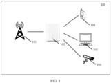
- FIG. 1 is a schematic diagram of an architecture of a mobile communications system applicable to an embodiment of this application.
- the mobile communications system 100 may include at least one network device 101, at least one CPE 102, and at least one user equipment (user equipment, UE) 103.
- FIG. 1 is merely a schematic diagram, and the communications system may further include other network devices, such as a wireless relay device and a wireless backhaul device, which are not shown in FIG. 1 .
- This embodiment of this application does not limit a quantity and specific types of network devices and UEs included in the mobile communications system.
- the UE 103 in this embodiment of this application may be a mobile phone, a tablet computer, a notebook computer, a smart band, a smartwatch, a smart helmet, smart glasses, or the like.
- the electronic device may be alternatively a cellular phone, a cordless phone, a session initiation protocol (session initiation protocol, SIP) phone, a wireless local loop (wireless local loop, WLL) station, a personal digital assistant (personal digital assistant, PDA), a handheld device having a wireless communication function, a computing device, another processing device connected to a wireless modem, a vehicle-mounted device, an electronic device in a 5G network, an electronic device in a future evolved public land mobile network (public land mobile network, PLMN), or the like.
- SIP session initiation protocol
- WLL wireless local loop
- PDA personal digital assistant
- the technical solution provided in this application is applicable to the UE 103 that uses one or more of the following communications technologies: a Bluetooth (Bluetooth, BT) communications technology, a global positioning system (global positioning system, GPS) communications technology, a wireless fidelity (wireless fidelity, Wi-Fi) communications technology, a global system for mobile communications (global system for mobile communications, GSM) communications technology, a wideband code division multiple access (wideband code division multiple access, WCDMA) communications technology, a long term evolution (long term evolution, LTE) communications technology, a 5G communications technology, and another future communications technology.
- a Bluetooth Bluetooth, BT
- GPS global positioning system
- Wi-Fi wireless fidelity
- GSM global system for mobile communications
- WCDMA wideband code division multiple access
- LTE long term evolution
- the network device 101 in this embodiment of this application may be a device configured to communicate with a terminal device, and the network device may be a network device (base transceiver station, BTS) in a GSM system or code division multiple access (code division multiple access, CDMA), or may be a network device (NodeB, NB) in a WCDMA system, or may be an evolved network device (evolutional nodeB, eNB or eNodeB) in an LTE system.
- BTS base transceiver station
- CDMA code division multiple access
- NodeB, NB network device
- evolutional nodeB, eNB or eNodeB evolved network device
- the network device may be a relay station, an access point, a vehicle-mounted device, a wearable device, a network device in a future 5G network (new generation NodeB, gNB or gNodeB) or a network device in a future evolved PLMN network, and a later network device that supports a 3rd generation partnership project (3GPP) protocol version.
- 3GPP 3rd generation partnership project
- the CPE 102 can connect the user equipment 103 to the Internet by receiving a cellular network signal sent by the network device 101 and transmitting the cellular network signal to the user equipment 103.
- the CPE 102 can convert, into a Wi-Fi signal, a 2G/3G/4G/5G signal transmitted by the network device 101, to connect the user equipment 103 to the Internet.
- the CPE 102 is usually located outdoors, and transmits a signal to the indoor user equipment 103 through a PoE network cable.
- the PoE network cable needs to pass through a window or a wall, and consequently, it is relatively difficult to arrange and route cables.
- a gap of a window of a user is small or there is no hole, on the wall, that can be borrowed, professional engineering installation and hole drilling are required, and installation costs are high.
- This application provides an electronic device that can be applied to the foregoing scenarios, and can wirelessly transmit, from the outdoors to the indoors, a cellular network signal sent by the network device. Therefore, it does not require the PoE network cable to pass through a window or a wall, and a need for professional engineering installation and hole drilling is eliminated. This can greatly improve user experience.
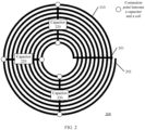
- FIG. 2 is a schematic diagram of an antenna structure according to an embodiment of this application, and the antenna structure may be applied to the CPE or UE in the scenario shown in FIG. 1 .
- the antenna structure 200 may include a coil 210 and at least one capacitor 220.
- the capacitor 220 may be connected in parallel to the coil 210.
- the parallel connection can be understood as follows: One end of the capacitor 220 is electrically connected to the coil 210 at an outer ring of the coil 210, and the other end of the capacitor 220 is electrically connected to the coil 210 at an inner ring of the coil 220, in other words, the capacitor 220 is connected in parallel to the coil 210.
- the outer ring of the coil 210 may be an outermost layer of coil of the coil 210, or may be one of several layers of coil adjacent to the outermost layer of coil. This may be selected based on an actual design or simulation. It should be understood that the inner ring of the coil 220 can also be understood correspondingly. In addition, the outer ring and the inner ring are relative concepts, to be specific, the outer ring is only required to be axially outside a location at which the inner ring is located.
- the coil 210 of this embodiment of this application is obtained by adding, to a conventional design, at least one capacitor 220 arranged in parallel.
- the capacitor 220 connected in parallel to the coil 210 is in an open-circuit state, and the parallelled connected capacitor 220 does not affect normal operation of the coil 210.
- the low-frequency mode is below 100 MHz.
- the coil 210 operating in the low-frequency mode may be a wireless charging coil or a near field communication (NFC) coil.
- NFC near field communication
- an operating frequency of the antenna structure 200 in the low-frequency mode is dozens of kHz.
- the coil 210 is an NFC coil
- the operating frequency of the antenna structure 200 in the low-frequency mode is 13.6 MHz.
- the capacitor 220 connected in parallel to the coil 210 is in a short-circuit state, so that conduction between the inner ring and the outer ring of the coil 210 can be ensured.
- voltages between inner rings and outer rings of the coil 210 are balanced, and the coil 210 as a whole may be used as an entity, may be used as a radiator operating in the high-frequency mode, and has good radiation features.
- the high-frequency mode is above 1 GHz.
- the coil 210 operating in the high-frequency mode may operate in a 2G/3G/4G/5G related frequency band, or may operate in a 2.4 GHz or 5 GHz Wi-Fi frequency band.
- a quantity of capacitors 220 connected in parallel to the coil 210 can be determined based on an actual design or simulation.
- a first end 201 and a second end 202 of the coil 210 may be electrically connected to a front-end circuit of an electronic device, for transmitting an electrical signal.
- the coil 210 is a wireless charging coil
- the first end 201 and the second end 202 may be electrically connected to a wireless charging module in the electronic device.
- the coil 210 is a high-frequency communications antenna
- the first end 201 may be electrically connected to a radio frequency module in the electronic device
- the second end 202 may be electrically connected to a reference ground in the electronic device.
- a capacitance value of the capacitor 220 may be between 0.5 pF and 5 pF.
- a capacitance value of the capacitor 220 may be 1 pF. It should be understood that the capacitance value of the capacitor 220 can be selected based on an actual design or simulation. This is not limited in this application.
- the capacitor 220 may be a distributed capacitor or a lumped capacitor.
- the capacitance value of the capacitor 220 may vary with a frequency radiated by the antenna structure, which can provide better matching for the antenna structure.
- a volume of the capacitor 220 is smaller, which is conducive to the miniaturization of the antenna structure.
- the plane size of the coil 210 is less than or equal to 80 mm ⁇ 80 mm, which is conducive to the miniaturization of the antenna structure.
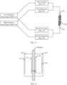
- FIG. 3 is a schematic diagram of a structure of an electronic device according to an embodiment of this application.
- the electronic device may include a low-frequency processing module 310, a high-frequency processing module 320, and an antenna structure 200, and the antenna structure 200 may be the foregoing antenna structure shown in FIG. 2 .
- the low-frequency processing module 310 may be separately electrically connected to the first end 201 and the second end 202 of the coil in the antenna structure 200.
- the high-frequency processing module 320 may be separately electrically connected to the first end 201 and the second end 202 of the coil in the antenna structure 200.
- the low-frequency processing module 310 can be configured to process an electrical signal used when capacitors connected in parallel in the antenna structure 200 are open-circuited, to be specific, can process an electrical signal with a frequency less than 100 MHz.
- the high-frequency processing module 320 can be configured to process an electrical signal used when capacitors connected in parallel in the antenna structure 200 are short-circuited, to be specific, can process an electrical signal with a frequency greater than 1 GHz.
- the antenna structure 200 when the antenna structure 200 operates in the high-frequency mode, in the high-frequency processing module 320, the antenna structure 200 may be electrically connected to a high-frequency processing circuit at the first end 201 of the coil, the second end 202 of the coil may be grounded, and a matching network can be added between the second end 202 and the ground. This can suppress currents in other frequency bands and increase overall performance of the antenna structure.
- the electronic device 300 may further include a first low-pass filter 330, a second low-pass filter 340, a first high-pass filter 350, and a second high-pass filter 360.
- the first low-pass filter 330 may be arranged between the low-frequency processing module 310 and the first end 201 of the coil in the antenna structure 200, and is electrically connected to the low-frequency processing module 310 and the antenna structure 200.
- the second low-pass filter 340 may be arranged between the low-frequency processing module 310 and the second end 202 of the coil in the antenna structure 200, and is electrically connected to the low-frequency processing module 310 and the antenna structure 200.
- the first high-pass filter 350 may be arranged between the low-frequency processing module 310 and the first end 201 of the coil in the antenna structure 200, and is electrically connected to the low-frequency processing module 310 and the antenna structure 200.
- the second high-pass filter 360 may be arranged between the low-frequency processing module 310 and the second end 202 of the coil in the antenna structure 200, and is electrically connected to the low-frequency processing module 310 and the antenna structure 200.
- a high-frequency channel and a low-frequency channel can be distinguished through a high-pass filter and a low-pass filter.
- a high-pass filter is arranged between the antenna structure 200 and the high-frequency processing module 320, and the antenna structure is open-circuited at a low frequency, which can prevent a crosstalk of low-frequency electrical signals to the high-frequency processing module 320.
- a low-pass filter is arranged between the antenna structure 200 and the low-frequency processing module 310, and the antenna structure is open-circuited at a high frequency, which can prevent a crosstalk of high-frequency electrical signals to the low-frequency processing module 310.
- the high-pass filter and the low-pass filter can be added to the electronic device, to effectively reduce a problem of signal interference.
- FIG. 4 is a schematic diagram of an application scenario of an electronic device according to an embodiment of this application.
- the CPE shown in FIG. 1 can be divided into an indoor unit (indoor unit, IDU) located indoors and an outdoor unit (outdoor unit, ODU) located outdoors. Therefore, the electronic device provided in this embodiment of this application may be an IDU or an ODU.
- a first electronic device 410 and a second electronic device 420 may be respectively located on two sides of an obstacle, and the first electronic device 410 and the second electronic device 420 are disposed opposite to each other.
- the obstacle may be a window or a wall.
- the first electronic device 410 and the second electronic device 420 are the electronic device shown in FIG. 3 .
- the first electronic device 410 may include a first antenna structure 411, a first low-frequency module, and a first high-frequency module.
- the second electronic device 420 may include a second antenna structure 421, a second low-frequency module, and a second high-frequency module.
- the first electronic device 410 may be an ODU and is arranged outdoors.
- the first antenna structure 411 may be a charging coil when operating in a low-frequency mode, and may be a communications antenna when operating in a high-frequency mode.
- a first low-frequency processing mode in the first electronic device 410 may be configured to process an electrical signal for wireless charging
- a first high-frequency processing module may be configured to process an electrical signal for data transmission.
- the second electronic device 420 may be an IDU and is arranged indoors.
- the second antenna structure 421 may be a charging coil when operating in a low-frequency mode, and may be a communications antenna when operating in a high-frequency mode.
- a second low-frequency processing mode in the second electronic device 320 may be configured to process an electrical signal for wireless charging
- a second high-frequency processing module may be configured to process an electrical signal for data transmission.
- the second antenna structure 421 of the second electronic device 420 can be used as a transmit charging coil, and the first antenna structure 411 of the first electronic device 410 can be used as a receive charging coil.
- the second electronic device 420 located indoors can process, by using the second low-frequency processing module, an electrical signal for wireless charging, send, by using the second antenna structure 421, an electrical signal for wireless charging to the first antenna structure 411, and power the first electronic device 410 by using the first low-frequency processing module. Therefore, the first electronic device 410 located outdoors can be powered by using the second electronic device 420, no additional power supply is required, and an internal structure of the first electronic device 410 is simpler.
- the electronic device 410 located outdoors can process, by using the first high-frequency processing module, an electrical signal that carries data, and send, to the second antenna structure 421 by using the first antenna structure 411, an electrical signal that carries data.
- the second electronic device 420 can obtain transmitted data. It should be understood that data transmission is bidirectional, and the second electronic device 420 also transmits data to the first electronic device 410 through a similar path.
- a distance L 1 between the first antenna structure 411 and the second antenna structure 421 may be less than 10 cm, and may be 5 cm.
- the distance L1 between the first antenna structure 411 and the second antenna structure 421 may be a horizontal distance between the first antenna structure 411 and the second antenna structure 421, or may be a straight-line distance between closest points on the first antenna structure 411 and the second antenna structure 421.
- plane sizes of the first antenna structure 411 and the second antenna structure 421 may be different, to be specific, diameters of a coil in the first antenna structure 311 and a coil in the second antenna structure 321 may be different. It should be understood that an adjustment can be made based on an actual design or a simulation result. This is not limited in this application.
- the first electronic device 410 may further include a first antenna unit 412, and an operating frequency band of the first antenna unit 412 may cover at least one frequency band in a cellular network, and may be used for data transmission with a network device.
- the cellular network may include 2G, 3G, 4G, 5G, or future communications systems.
- the second electronic device 420 may further include a second antenna unit 422, and an operating frequency band of the second antenna unit 422 may cover a Wi-Fi frequency band, and may be used for data transmission with indoor user equipment.
- the Wi-Fi frequency band may be at least one of a 2.4 GHz or 5 G frequency band.
- a cellular network signal may be converted into a Wi-Fi signal through the first electronic device 410 and the second electronic device 420, and a cellular network signal sent by the network device can be wirelessly transmitted from the outdoors to the indoors. Therefore, it does not require the PoE network cable to pass through a window or a wall, and a need for professional engineering installation and hole drilling is eliminated. This is convenient and quick, and greatly improves user experience.
- the second antenna unit 422 may be alternatively the antenna structure shown in FIG. 2 .
- the second antenna unit 422 may be an NFC coil when operating in a low-frequency mode, and when operating in a high-frequency mode, may be an antenna operating in a Wi-Fi frequency band.
- a corresponding low-frequency processing module of the second antenna unit 422 may be configured to process an electrical signal for NFC
- a corresponding high-frequency processing module may be configured to process an electrical signal for a Wi-Fi frequency band.
- the electronic device provided in this embodiment of this application may be alternatively the user equipment shown in FIG. 1 , and the user equipment may include the antenna structure shown in FIG. 2 .
- the antenna structure an NFC coil and a Wi-Fi antenna can be combined to reduce a quantity of antennas in the user equipment and provide a larger arrangement space for antennas operating in other frequency bands.
- the indoor user equipment is within a specific range of the second antenna unit 322, the user equipment can obtain a Wi-Fi password through NFC, which is more convenient and conducive to improving user experience.
- the coil provided in this embodiment of this application through a design of connecting a capacitor in parallel and by using a characteristic that the capacitor is short-circuited at a high frequency and short-circuited at a low frequency, the coil can operate at a high frequency and a low frequency at the same time.
- the high-frequency processing module and the low-frequency processing module respectively process signals at the two frequencies. Therefore, the coil provided in this embodiment of this application may alternatively be another low-frequency communications coil, and is not only limited to a wireless charging coil or an NFC coil.
- FIG. 5 and FIG. 6 are schematic diagrams of S-parameter simulation between the first antenna structure and the second antenna structure shown in FIG. 4 .
- FIG. 5 is a schematic diagram of S-parameter simulation used when no capacitor is connected in parallel to a coil.
- FIG. 6 is a schematic diagram of S-parameter simulation used when a capacitor is connected in parallel to a coil.
- a port 1 may be a connection port between the coil and the high-frequency processing module in the first antenna structure of the first electronic device
- a port 2 may be a connection port between the coil and the high-frequency processing module in the second antenna structure of the second electronic device.
- a larger parameter S12 indicates more electrical signals transmitted from the port 2 to the port 1, and indicates better signal transmission performance between the first antenna structure and the second antenna structure.
- a smaller parameter S11 indicates smaller reflection at the port 1, and indicates more electrical signals transmitted to the port 2.
- a smaller parameter S22 indicates smaller reflection at the port 2, and indicates more electrical signals transmitted to the port 1.
- the disclosed system, apparatus, and method may be implemented in another manner.
- the described apparatus embodiment is merely an example.
- division into the units is merely logical function division and may be other division in actual implementation.
- a plurality of units or components may be combined or integrated into another system, or some features may be ignored or not performed.
- the displayed or discussed mutual couplings or direct couplings or communication connections may be implemented through some interfaces.
- the indirect couplings or communication connections between the apparatuses or units may be implemented in electronic or other forms.
Landscapes
- Engineering & Computer Science (AREA)
- Computer Networks & Wireless Communication (AREA)
- Signal Processing (AREA)
- Power Engineering (AREA)
- Near-Field Transmission Systems (AREA)
Applications Claiming Priority (2)
| Application Number | Priority Date | Filing Date | Title |
|---|---|---|---|
| CN202010684519.1A CN113949407B (zh) | 2020-07-16 | 2020-07-16 | 一种电子设备及天线结构 |
| PCT/CN2021/105035 WO2022012391A1 (zh) | 2020-07-16 | 2021-07-07 | 一种电子设备及天线结构 |
Publications (2)
| Publication Number | Publication Date |
|---|---|
| EP4170823A1 true EP4170823A1 (de) | 2023-04-26 |
| EP4170823A4 EP4170823A4 (de) | 2023-12-27 |
Family
ID=79326785
Family Applications (1)
| Application Number | Title | Priority Date | Filing Date |
|---|---|---|---|
| EP21842642.7A Pending EP4170823A4 (de) | 2020-07-16 | 2021-07-07 | Elektronische vorrichtung und antennenstruktur |
Country Status (5)
| Country | Link |
|---|---|
| US (1) | US20230275603A1 (de) |
| EP (1) | EP4170823A4 (de) |
| JP (1) | JP7605959B2 (de) |
| CN (2) | CN116633392A (de) |
| WO (1) | WO2022012391A1 (de) |
Family Cites Families (19)
| Publication number | Priority date | Publication date | Assignee | Title |
|---|---|---|---|---|
| JP2004356765A (ja) * | 2003-05-27 | 2004-12-16 | Matsushita Electric Ind Co Ltd | 共振周波数調整装置、非接触リーダライタ、および、非接触データキャリアシステム |
| US8934984B2 (en) * | 2007-05-31 | 2015-01-13 | Cochlear Limited | Behind-the-ear (BTE) prosthetic device with antenna |
| WO2010001469A1 (ja) * | 2008-07-02 | 2010-01-07 | 三菱電機株式会社 | 無線通信装置 |
| US8344959B2 (en) * | 2009-04-30 | 2013-01-01 | Nokia Corporation | Multiprotocol antenna for wireless systems |
| JP5511071B2 (ja) * | 2010-07-07 | 2014-06-04 | Necトーキン株式会社 | アンテナモジュール及び非接触電力伝送装置 |
| JP5803550B2 (ja) * | 2011-10-14 | 2015-11-04 | ソニー株式会社 | アンテナ回路、通信装置、および通信方法 |
| JP2013090172A (ja) * | 2011-10-19 | 2013-05-13 | Sharp Corp | 無線回路 |
| JP5988146B2 (ja) * | 2011-11-15 | 2016-09-07 | パナソニックIpマネジメント株式会社 | 伝送コイル及び携帯無線端末 |
| US9125007B2 (en) * | 2012-03-30 | 2015-09-01 | Intel Corporation | Near field communications (NFC) coil with embedded wireless antenna |
| DE102013111027A1 (de) * | 2013-10-04 | 2015-04-09 | Infineon Technologies Ag | Mehrfrequenzfähige Antenne für miniaturisierte Anwendungen |
| KR101672035B1 (ko) * | 2015-02-17 | 2016-11-03 | 조인셋 주식회사 | 안테나 대역폭 확장장치 |
| WO2017014467A1 (ko) * | 2015-07-20 | 2017-01-26 | 주식회사 아모텍 | 콤보 안테나모듈 및 이를 포함하는 휴대용 전자장치 |
| CN105071055B (zh) * | 2015-07-28 | 2018-12-28 | 福建联迪商用设备有限公司 | 一种防高频干扰的rf天线阻抗匹配电路及其设计方法 |
| CN205159514U (zh) * | 2015-11-19 | 2016-04-13 | 上海仪电智能电子有限公司 | 一种双频智能标签天线 |
| CN205921075U (zh) * | 2016-07-14 | 2017-02-01 | 浙江生辉照明有限公司 | Fm天线、nfc天线、多功能天线和照明设备 |
| KR102565276B1 (ko) * | 2016-11-16 | 2023-08-09 | 삼성전자주식회사 | 코일 공유 구조를 가지는 무선 장치 |
| JP6855878B2 (ja) * | 2017-03-29 | 2021-04-07 | 富士通株式会社 | 受電器、電力伝送システム、及び、受電器の制御方法 |
| CN108649671B (zh) * | 2018-04-26 | 2021-05-04 | Oppo广东移动通信有限公司 | 一种无线充电电路及可穿戴式设备 |
| CN110730021B (zh) * | 2019-08-31 | 2022-10-25 | 荣耀终端有限公司 | 一种无线控制方法及设备 |
-
2020
- 2020-07-16 CN CN202310610495.9A patent/CN116633392A/zh active Pending
- 2020-07-16 CN CN202010684519.1A patent/CN113949407B/zh active Active
-
2021
- 2021-07-07 JP JP2023502831A patent/JP7605959B2/ja active Active
- 2021-07-07 WO PCT/CN2021/105035 patent/WO2022012391A1/zh not_active Ceased
- 2021-07-07 US US18/005,538 patent/US20230275603A1/en active Pending
- 2021-07-07 EP EP21842642.7A patent/EP4170823A4/de active Pending
Also Published As
| Publication number | Publication date |
|---|---|
| CN113949407B (zh) | 2023-06-20 |
| WO2022012391A1 (zh) | 2022-01-20 |
| JP2023533355A (ja) | 2023-08-02 |
| CN113949407A (zh) | 2022-01-18 |
| JP7605959B2 (ja) | 2024-12-24 |
| EP4170823A4 (de) | 2023-12-27 |
| CN116633392A (zh) | 2023-08-22 |
| US20230275603A1 (en) | 2023-08-31 |
Similar Documents
| Publication | Publication Date | Title |
|---|---|---|
| CN215911582U (zh) | 折叠终端 | |
| KR102343011B1 (ko) | 멀티 웨이 스위치, 무선 주파수 시스템 및 통신 장치 | |
| US10498039B2 (en) | Base station | |
| US12597696B2 (en) | Package antenna apparatus and wireless communication apparatus | |
| WO2019174253A1 (en) | Multiway switch, radio frequency system, and wireless communication device | |
| WO2019174283A1 (en) | Multiway switch, radio frequency system, and communication device | |
| CN105706371A (zh) | 用于防止传送器泄露的方法和设备 | |
| CN112838351A (zh) | 一种射频装置和电子设备 | |
| WO2017173582A1 (zh) | 终端天线和终端 | |
| EP4170823A1 (de) | Elektronische vorrichtung und antennenstruktur | |
| WO2015176427A1 (zh) | 一种射频收发方法及系统 | |
| CN117158019A (zh) | 集成式宏下一代无线电单元的系统和设计方法 | |
| CN203775416U (zh) | 基站 | |
| CN101295817A (zh) | 天线模块及其应用的装置 | |
| CN223758270U (zh) | 无线接入点装置 | |
| CN103546177B (zh) | 射频接收装置及车载空口监测设备 | |
| EP3182618A1 (de) | Vorrichtung zum verringern einer magnetischen kupplung zwischen einer ersten elektronischen schaltung und einer zweiten elektronischen schaltung | |
| WO2026081947A1 (zh) | 一种通信装置和通信方法 | |
| KR101682292B1 (ko) | 더미 케이블을 이용한 격리도 향상을 위한 장치 | |
| CN104065162A (zh) | 一种专用于输电线路监测装置互联的双频、远距离传输无线通信系统 | |
| CN115549700A (zh) | 传输信号的装置及其方法 | |
| HK1252761A1 (zh) | 多路选择开关、射频系统以及无线通信设备 | |
| HK1251731A1 (zh) | 多路选择开关、射频系统以及无线通信设备 | |
| HK1252761B (zh) | 多路选择开关、射频系统以及无线通信设备 |
Legal Events
| Date | Code | Title | Description |
|---|---|---|---|
| STAA | Information on the status of an ep patent application or granted ep patent |
Free format text: STATUS: THE INTERNATIONAL PUBLICATION HAS BEEN MADE |
|
| PUAI | Public reference made under article 153(3) epc to a published international application that has entered the european phase |
Free format text: ORIGINAL CODE: 0009012 |
|
| STAA | Information on the status of an ep patent application or granted ep patent |
Free format text: STATUS: REQUEST FOR EXAMINATION WAS MADE |
|
| 17P | Request for examination filed |
Effective date: 20230123 |
|
| AK | Designated contracting states |
Kind code of ref document: A1 Designated state(s): AL AT BE BG CH CY CZ DE DK EE ES FI FR GB GR HR HU IE IS IT LI LT LU LV MC MK MT NL NO PL PT RO RS SE SI SK SM TR |
|
| DAV | Request for validation of the european patent (deleted) | ||
| DAX | Request for extension of the european patent (deleted) | ||
| REG | Reference to a national code |
Ref country code: DE Ref legal event code: R079 Free format text: PREVIOUS MAIN CLASS: H01Q0007000000 Ipc: H04B0005000000 |
|
| A4 | Supplementary search report drawn up and despatched |
Effective date: 20231124 |
|
| RIC1 | Information provided on ipc code assigned before grant |
Ipc: H05K 9/00 20060101ALI20231120BHEP Ipc: H01Q 7/00 20060101ALI20231120BHEP Ipc: H04B 5/00 20060101AFI20231120BHEP |
|
| STAA | Information on the status of an ep patent application or granted ep patent |
Free format text: STATUS: EXAMINATION IS IN PROGRESS |
|
| 17Q | First examination report despatched |
Effective date: 20260304 |