EP4170902A1 - Vorspannungsschaltung für verarmungsbetrieb-verstärker - Google Patents
Vorspannungsschaltung für verarmungsbetrieb-verstärker Download PDFInfo
- Publication number
- EP4170902A1 EP4170902A1 EP22213788.7A EP22213788A EP4170902A1 EP 4170902 A1 EP4170902 A1 EP 4170902A1 EP 22213788 A EP22213788 A EP 22213788A EP 4170902 A1 EP4170902 A1 EP 4170902A1
- Authority
- EP
- European Patent Office
- Prior art keywords
- circuit
- current source
- current
- transistor
- potential
- Prior art date
- Legal status (The legal status is an assumption and is not a legal conclusion. Google has not performed a legal analysis and makes no representation as to the accuracy of the status listed.)
- Pending
Links
Images

Classifications
-
- H—ELECTRICITY
- H03—ELECTRONIC CIRCUITRY
- H03F—AMPLIFIERS
- H03F1/00—Details of amplifiers with only discharge tubes, only semiconductor devices or only unspecified devices as amplifying elements
- H03F1/30—Modifications of amplifiers to reduce influence of variations of temperature or supply voltage or other physical parameters
- H03F1/303—Modifications of amplifiers to reduce influence of variations of temperature or supply voltage or other physical parameters using a switching device
-
- H—ELECTRICITY
- H03—ELECTRONIC CIRCUITRY
- H03F—AMPLIFIERS
- H03F3/00—Amplifiers with only discharge tubes or only semiconductor devices as amplifying elements
- H03F3/189—High-frequency amplifiers, e.g. radio frequency amplifiers
- H03F3/19—High-frequency amplifiers, e.g. radio frequency amplifiers with semiconductor devices only
- H03F3/195—High-frequency amplifiers, e.g. radio frequency amplifiers with semiconductor devices only in integrated circuits
-
- H—ELECTRICITY
- H03—ELECTRONIC CIRCUITRY
- H03F—AMPLIFIERS
- H03F3/00—Amplifiers with only discharge tubes or only semiconductor devices as amplifying elements
- H03F3/189—High-frequency amplifiers, e.g. radio frequency amplifiers
- H03F3/19—High-frequency amplifiers, e.g. radio frequency amplifiers with semiconductor devices only
- H03F3/193—High-frequency amplifiers, e.g. radio frequency amplifiers with semiconductor devices only with field-effect devices
-
- H—ELECTRICITY
- H03—ELECTRONIC CIRCUITRY
- H03F—AMPLIFIERS
- H03F3/00—Amplifiers with only discharge tubes or only semiconductor devices as amplifying elements
- H03F3/20—Power amplifiers, e.g. Class B amplifiers, Class C amplifiers
- H03F3/21—Power amplifiers, e.g. Class B amplifiers, Class C amplifiers with semiconductor devices only
- H03F3/213—Power amplifiers, e.g. Class B amplifiers, Class C amplifiers with semiconductor devices only in integrated circuits
-
- H—ELECTRICITY
- H03—ELECTRONIC CIRCUITRY
- H03F—AMPLIFIERS
- H03F3/00—Amplifiers with only discharge tubes or only semiconductor devices as amplifying elements
- H03F3/72—Gated amplifiers, i.e. amplifiers which are rendered operative or inoperative by means of a control signal
-
- H—ELECTRICITY
- H03—ELECTRONIC CIRCUITRY
- H03F—AMPLIFIERS
- H03F1/00—Details of amplifiers with only discharge tubes, only semiconductor devices or only unspecified devices as amplifying elements
- H03F1/30—Modifications of amplifiers to reduce influence of variations of temperature or supply voltage or other physical parameters
- H03F1/301—Modifications of amplifiers to reduce influence of variations of temperature or supply voltage or other physical parameters in MOSFET amplifiers
-
- H—ELECTRICITY
- H03—ELECTRONIC CIRCUITRY
- H03F—AMPLIFIERS
- H03F2200/00—Indexing scheme relating to amplifiers
- H03F2200/18—Indexing scheme relating to amplifiers the bias of the gate of a FET being controlled by a control signal
-
- H—ELECTRICITY
- H03—ELECTRONIC CIRCUITRY
- H03F—AMPLIFIERS
- H03F2200/00—Indexing scheme relating to amplifiers
- H03F2200/258—Indexing scheme relating to amplifiers the input of the amplifier has voltage limiting means
-
- H—ELECTRICITY
- H03—ELECTRONIC CIRCUITRY
- H03F—AMPLIFIERS
- H03F2200/00—Indexing scheme relating to amplifiers
- H03F2200/27—A biasing circuit node being switched in an amplifier circuit
-
- H—ELECTRICITY
- H03—ELECTRONIC CIRCUITRY
- H03F—AMPLIFIERS
- H03F2200/00—Indexing scheme relating to amplifiers
- H03F2200/451—Indexing scheme relating to amplifiers the amplifier being a radio frequency amplifier
-
- H—ELECTRICITY
- H03—ELECTRONIC CIRCUITRY
- H03F—AMPLIFIERS
- H03F2203/00—Indexing scheme relating to amplifiers with only discharge tubes or only semiconductor devices as amplifying elements covered by H03F3/00
- H03F2203/72—Indexing scheme relating to gated amplifiers, i.e. amplifiers which are rendered operative or inoperative by means of a control signal
- H03F2203/7203—Indexing scheme relating to gated amplifiers, i.e. amplifiers which are rendered operative or inoperative by means of a control signal the gated amplifier being switched on or off by a switch in the bias circuit of the amplifier controlling a bias current in the amplifier
Definitions
- This disclosure relates generally to bias circuitry and more particularly to bias circuitry for depletion mode amplifiers.
- RF power amplifiers using depletion mode transistors to amplify an input radio frequency signal often use solid state "drain” switches to turn on and off DC supply power.
- An alternative to the drain switch is the gate switch, where a sufficiently negative voltage is supplied to the power amplifier's transistor gate to reduce the DC quiescent current to zero and also provide sufficient isolation in the RF path.
- An advantage of the gate switch approach is faster switching times between RF enable and off for systems using RF amplifiers.
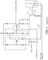
- One such circuit ( FIG. 1 ) is shown in US 6,600,301 B1, issued July 29, 2003 , inventor DeFalco, assigned to the same assignee as the present invention. While such circuit has been found to be effective in many applications, in applications having a wide variation in temperature and power supply, a sufficient off-state voltage must be applied to it to establish proper quiescent bias for proper RF amplifier operation inclusive of process, temperature, and power supply variations.
- CMOS complementary Silicon Oxide Semiconductor
- a circuit comprising: an amplifier, comprising: a depletion mode transistor having a source electrode coupled to a reference potential; a drain electrode coupled to a potential more positive than the reference potential; and a gate electrode for coupling to an input signal.
- the circuit includes a bias circuit, comprising: a current source; and biasing circuitry coupled to the current source and between the potential more positive than the reference potential and a potential more negative than the reference potential.
- a control circuit is connected to the current source for controlling the amount of current produced by the current source to the biasing circuitry.
- control circuit comprises a switch fed by a control signal to selectively place the switch in either an "on “condition” to enable current from the current source to pass to the biasing circuitry producing a bias voltage at the gate electrode of the transistor, or, an "off condition electrically inhibit current from the current source to the biasing circuitry removing the bias voltage from the from the bias circuit removing the current source and the bias voltage at the gate electrode of the transistor.
- control circuit varies the amount of current passing from the current source to the biasing circuitry in accordance with a control signal fed to the control circuit to corresponding vary a bias voltage at the gate electrode of the transistor.
- control signal diverts current produced by the current source from the biasing circuit in accordance with the control signal.
- control circuit is able to be implemented with relatively low voltage supplies and is able to control GaN bias with submicron Si CMOS operated in less than 2.5V..
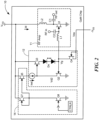
- a circuit 10 having an amplifier 11, here a radio frequency (RF Amp), comprising: a depletion mode transistor Q1 having a source electrode coupled to a reference potential, here ground; a drain electrode coupled to a potential more positive than the reference potential, here (+Vdd) through an inductor L2, as shown, the drain electrode providing an amplified RF output after passing through a capacitor, C1, as shown; and a gate electrode for coupling to an input signal, here an RF input through a capacitor, C2, as shown.
- RF Amp radio frequency
- the circuit 10 includes a bias circuit 12, comprising: a current mirror having: a current source I ref , and biasing circuitry (depletion mode transistors Q2, Q3, and Q4 and diodes Dn) arranged as shown, coupled to the current source I ref , and between the potential more positive than the reference potential (+Vdd) and a potential more negative than the reference potential; coupled to a potential more negative than the reference potential (-Vss).
- the diodes Dn is a series of a plurality n of diodes GaN diodes Dn, where n is the number of diodes in the series selected in accordance with the voltages used, here for example, Vdd is 24 volts and -Vss is -8.0 volts.
- the circuit 10 includes a control circuit 14, here depletion mode transistors Q5, Q7 and Q8, connected between the potential more positive than the reference potential (+Vdd) and the current source, I ref for controlling the amount of current passing from the current source I ref to the biasing circuitry 12 (depletion mode transistors Q2, Q3 and Q4).
- the control circuit 14 comprises a switch, here depletion mode transistors Q8, Q7, Q5 connected between the potential more positive than the reference potential (+Vdd) and the current source I ref .
- the drain of transistor Q8 is connected to the gate of transistor Q7, the source of transistor Q7 and the gate of transistor Q5.
- a control signal here either a logic 1, (here 0 volts) or a logic 0 (here -3.3 volts), is fed to the gate of transistor Q8, where the threshold voltage of Q8 is here -3.0 volts.
- transistor Q8 In response to a logic 0 signal, transistor Q8 is placed in the "off' or non-conducting condition and therefore transistor Q5 in the “on” or conducting condition and thus switch 14 is in the “on” condition.
- transistor Q8 is placed in the "on” or conducting condition and transistor Q5 is in the "off” or non-conducting condition and thus switch 14 is in the "off” condition.
- switch 14 when switch 14 is in the "on” condition, more particularly, when the gate of depletion mode transistor Q8 is in the “off “condition” in response to the logic 0 signal at its gate, transistor Q5 is in the “on” condition and thus switch 14 electrically connects the potential more positive than the reference potential (+Vdd) to the current source I ref so that current flows from the current source I ref to the biasing circuitry depletion mode transistors Q2, Q3 and Q4, producing a bias voltage at the gate electrode of the transistor Q1.
- switch 14 when switch 14 is in the "off' condition, more particularly, when the gate of depletion mode transistor Q8 is in the “on “condition” in response to the logic 1 signal at its gate, transistor Q5 is in the “off” condition and thus switch 14 electrically decouples the potential more positive than the reference potential (+Vdd) from the bias circuit 12 inhibiting or preventing current flow from the current source I ref to the biasing circuitry removing the current source Iref and hence the bias from the gate electrode of the transistor Q1 .
- the output of the bias circuit 12 is fed to the gate electrode of depletion mode transistor through an inductor L1, as shown; it being noted that the deletion mode transistor Q4 is a diode connected transistor and couples the gate electrode of transistor Q1 to the potential more negative than the reference potential (-Vss), as shown.
- the circuit is a D-mode current mirror circuit for quiescent bias control of GaN amplifiers
- Q2 is a Gallium Nitride (GaN) mirror FET and Q1 is the GaN HEMT used in the RF amplifier.
- the reference current source Iref drawn in to Q2 controls the quiescent current Id of Q1.
- the current source I ref may be a saturated resistor as described in U. S. Patent No. 8,854,140 or a linear resistor, transistor or from an off chip reference if needed.
- Transistor Q5 is sized such that it stays in linear operation relative to Iref so that it accommodates the amount of current produced by the current source Iref.
- the circuit shown in FIG. 2 has the following features:
- a circuit 20 is shown here having as the control circuit 22 that varies the amount of current, Ictrl, is diverted from the current source Q10 (Is) to biasing circuitry 24 selectively in accordance with a control signal fed to the control circuit to corresponding vary a bias voltage at the gate electrode of the transistor, Q1.
- the control circuit 22 controls a GaN HEMT bias circuit 24 formed on a Group III-V chip, here a GaN chip, using submicron Silicon (Si) CMOS current Digital to Analog Converter (DAC) formed on a silicon chip.
- the circuit 24 on the right is in GaN HEMT technology, that is formed using a GaN chip.
- Depletion mode transistor Q10 provides a constant current source, Is.
- Depletion mode transistor Q2 is the GaN mirror FET and depletion mode transistor Q1 is the GaN HEMT used in the RF amplifier 24.
- transistor Q2 needs to be in saturation mode.
- voltage Vd2 should be about 5V or higher.
- Vd2 is set by transistor Q3 and a series of a plurality n of diodes GaN diodes Dn, where n is the number of diodes in the series selected in accordance with the voltages used, here for example, Vdd is 24 volts and -Vss is -8.0 volts.
- the voltage drop across each of the n diodes Dn is set by current source of Q1 1 which, as will be shown, is controlled by a control signal CNTLR fed to a Digital to Analog Converter (DAC).
- the source of the control signal may be, for example, an analog signal related to the temperature of the GaN chip.
- the amount of current Ictrl passing though the diodes Dm that is the amount of current bled from the current source Q10, Is, is a function of the control signal CNTLR fed to the DAC.
- the circuit 22 on the left in FIG. 3 is in a submicron Si CMOS technology that is formed on a silicon chip.
- the control current 22 controls the amount of current Ictrl bled or drawn from the current source Is.
- the control signal CTRLR diverts current Is produced by the current source, transistor Q10, from the biasing circuit in accordance with the control signal.
- Iref the amount of current produced by the current source Q10 and fed to the biasing circuitry 25, here interconnected transistors Q2, Q3 and diodes Dn and Ictrl is the amount of current produced by the current source Q 10 and diverted to the control circuit 22, more particularly diodes Dm and transistor Q11.
- the control circuit 22 is able to be implemented with relatively low voltage supplies, Vcc.
- CMOS control circuit 22 Ictrl is thus controlled by a standard current CMOS Digital to Analog Converter (DAC) coupled between Vcc and current mirror made up of diode connected NMOS transistor Q12 and NMOS transistor Q11, connected as shown.
- DAC Digital to Analog Converter
- the CMOS circuit 22 is supplied by the standard CMOS supply voltage, Vcc, usually 2.5V or less. For deep submicron CMOS technology, the supply voltage can be 1.5V or lower.
- a series of Si diodes Dm is used to connect the drain of NMOS FET Q11 to the drain of GaN HEMT Q2.
- the Si diodes Dm can be easily formed using NMOS FET or lateral PNP transistor offered in standard CMOS process. These diodes Dm lower the voltage of Vd2 ( ⁇ >5V) to the safe drain voltage of Vd6, typically above 0.5V and less than 3V, depending on the CMOS technology used.
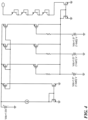
- FIG. 4 shows the implementation of a control circuit on a 0.13um Si CMOS process.
- the output current is controlled by a current DAC supplied by 1.5V.
- lateral PNP or VPNP transistors are used to form Si diodes Dm to level shift the output voltage.
- circuit shown in FIG. 3 has the following features:
- a circuit includes: an amplifier, comprising: a depletion mode transistor having a source electrode coupled to a reference potential; a drain electrode coupled to a potential more positive than the reference potential; and a gate electrode for coupling to an input signal; a bias circuit, comprising: a current source; and biasing circuitry coupled to the current source and between the potential more positive than the reference potential and a potential more negative than the reference potential; and a control circuit connected to the current source for controlling the amount of current produced by the current source to the biasing circuitry.
- the circuit may include one or more of the following features, individually or in combination to include: wherein the control circuit comprises a switch fed by a control signal to selectively place the switch in either an "on "condition” to enable current from the current source to pass to the biasing circuitry producing a bias voltage at the gate electrode of the transistor, or, an "off condition electrically inhibit current from the current source to the biasing circuitry removing the bias voltage from the from the bias circuit removing the current source and the bias voltage at the gate electrode of the transistor; wherein the control circuit varies the amount of current passing from the current source to the biasing circuitry in accordance with a control signal fed to the control circuit to corresponding vary a bias voltage at the gate electrode of the transistor; wherein the switch comprises a second depletion mode field effect transistor and wherein a gate electrode of the second depletion mode field effect transistor is fed the control signal; wherein the biasing circuitry comprises a plurality of additional depletion mode field effect transistors; wherein the amplifier and bias circuit are formed on a Group III-V chip and
Landscapes
- Engineering & Computer Science (AREA)
- Power Engineering (AREA)
- Microelectronics & Electronic Packaging (AREA)
- Amplifiers (AREA)
Applications Claiming Priority (4)
| Application Number | Priority Date | Filing Date | Title |
|---|---|---|---|
| US201562181713P | 2015-06-18 | 2015-06-18 | |
| US15/175,610 US9960740B2 (en) | 2015-06-18 | 2016-06-07 | Bias circuitry for depletion mode amplifiers |
| EP16733245.1A EP3311483B1 (de) | 2015-06-18 | 2016-06-09 | Vorspannungsschaltung für verstärker vom verarmungstyp |
| PCT/US2016/036546 WO2016205049A1 (en) | 2015-06-18 | 2016-06-09 | Bias circuitry for depletion mode amplifiers |
Related Parent Applications (2)
| Application Number | Title | Priority Date | Filing Date |
|---|---|---|---|
| EP16733245.1A Division EP3311483B1 (de) | 2015-06-18 | 2016-06-09 | Vorspannungsschaltung für verstärker vom verarmungstyp |
| EP16733245.1A Division-Into EP3311483B1 (de) | 2015-06-18 | 2016-06-09 | Vorspannungsschaltung für verstärker vom verarmungstyp |
Publications (1)
| Publication Number | Publication Date |
|---|---|
| EP4170902A1 true EP4170902A1 (de) | 2023-04-26 |
Family
ID=56289581
Family Applications (2)
| Application Number | Title | Priority Date | Filing Date |
|---|---|---|---|
| EP16733245.1A Active EP3311483B1 (de) | 2015-06-18 | 2016-06-09 | Vorspannungsschaltung für verstärker vom verarmungstyp |
| EP22213788.7A Pending EP4170902A1 (de) | 2015-06-18 | 2016-06-09 | Vorspannungsschaltung für verarmungsbetrieb-verstärker |
Family Applications Before (1)
| Application Number | Title | Priority Date | Filing Date |
|---|---|---|---|
| EP16733245.1A Active EP3311483B1 (de) | 2015-06-18 | 2016-06-09 | Vorspannungsschaltung für verstärker vom verarmungstyp |
Country Status (4)
| Country | Link |
|---|---|
| US (2) | US9960740B2 (de) |
| EP (2) | EP3311483B1 (de) |
| CN (1) | CN107750430B (de) |
| WO (1) | WO2016205049A1 (de) |
Families Citing this family (7)
| Publication number | Priority date | Publication date | Assignee | Title |
|---|---|---|---|---|
| US9960740B2 (en) | 2015-06-18 | 2018-05-01 | Raytheon Company | Bias circuitry for depletion mode amplifiers |
| US10263566B1 (en) | 2017-09-28 | 2019-04-16 | Raytheon Company | Radio frequency power amplifier |
| US10447208B2 (en) * | 2017-12-15 | 2019-10-15 | Raytheon Company | Amplifier having a switchable current bias circuit |
| US12278600B2 (en) | 2021-12-28 | 2025-04-15 | Raytheon Company | Amplifier bias circuit |
| US20230299720A1 (en) * | 2022-03-15 | 2023-09-21 | Nxp Usa, Inc. | Power amplifier bias circuit |
| US12261571B2 (en) | 2022-03-28 | 2025-03-25 | Nxp Usa, Inc. | Bias control circuit for power transistors |
| US12592673B2 (en) | 2023-03-17 | 2026-03-31 | Raytheon Company | Off-state isolation bias circuit for D-mode amplifiers |
Citations (6)
| Publication number | Priority date | Publication date | Assignee | Title |
|---|---|---|---|---|
| WO1997023037A1 (en) * | 1995-12-15 | 1997-06-26 | Anadigics, Inc. | Amplifier using a single polarity power supply |
| WO1998038733A1 (en) * | 1997-02-26 | 1998-09-03 | Ericsson Inc. | Flexible current control in power amplifiers |
| US6600301B1 (en) | 2002-04-30 | 2003-07-29 | Raytheon Company | Current shutdown circuit for active bias circuit having process variation compensation |
| US20100039168A1 (en) * | 2008-08-12 | 2010-02-18 | Bettencourt John P | Bias network |
| US8854140B2 (en) | 2012-12-19 | 2014-10-07 | Raytheon Company | Current mirror with saturated semiconductor resistor |
| EP2816729A1 (de) * | 2013-06-21 | 2014-12-24 | International Rectifier Corporation | Verarmungsmodus-Gruppe-III-V-Transistor mit Hochspannungs-Gruppe-IV-Freigabeschalter |
Family Cites Families (20)
| Publication number | Priority date | Publication date | Assignee | Title |
|---|---|---|---|---|
| US3506932A (en) | 1968-02-28 | 1970-04-14 | Bell Telephone Labor Inc | Quadrature hybrid coupler |
| US4743862A (en) | 1986-05-02 | 1988-05-10 | Anadigics, Inc. | JFET current mirror and voltage level shifting apparatus |
| US4896121A (en) | 1988-10-31 | 1990-01-23 | Hughes Aircraft Company | Current mirror for depletion-mode field effect transistor technology |
| EP0682381A1 (de) | 1994-05-02 | 1995-11-15 | E-Systems Inc. | Breitband-Richtkoppler |
| US6114912A (en) * | 1999-04-22 | 2000-09-05 | Lucent Technologies Inc. | Integrated amplifier having a voltage-controlled current source |
| US6559722B1 (en) * | 1999-08-10 | 2003-05-06 | Anadigics, Inc. | Low bias current/temperature compensation current mirror for linear power amplifier |
| US6831517B1 (en) | 2002-12-23 | 2004-12-14 | Intersil Americas, Inc. | Bias-management system and method for programmable RF power amplifier |
| EP1503447B1 (de) | 2003-07-31 | 2005-09-14 | Alcatel | Richtkoppler mit einem Einstellmittel |
| US7562581B2 (en) * | 2005-09-29 | 2009-07-21 | Case Western Reserve University | Wireless sensor platform for harsh environments |
| JP4749105B2 (ja) * | 2005-09-29 | 2011-08-17 | 新日本無線株式会社 | 基準電圧発生回路 |
| US8017978B2 (en) | 2006-03-10 | 2011-09-13 | International Rectifier Corporation | Hybrid semiconductor device |
| CN101399546B (zh) * | 2007-09-26 | 2010-11-10 | 中芯国际集成电路制造(上海)有限公司 | 数模转换单元和电路 |
| JP2010041370A (ja) * | 2008-08-05 | 2010-02-18 | Nec Electronics Corp | 演算増幅回路及び表示パネル駆動装置 |
| JP2010278521A (ja) | 2009-05-26 | 2010-12-09 | Mitsubishi Electric Corp | 電力増幅器 |
| US7876157B1 (en) * | 2009-08-04 | 2011-01-25 | Skyworks Solutions, Inc. | Power amplifier bias circuit having controllable current profile |
| WO2013088635A1 (ja) * | 2011-12-15 | 2013-06-20 | パナソニック株式会社 | 高出力電力増幅器 |
| US8643521B1 (en) * | 2012-11-28 | 2014-02-04 | United Microelectronics Corp. | Digital-to-analog converter with greater output resistance |
| CN103474015B (zh) * | 2013-08-20 | 2016-08-17 | 北京大学深圳研究生院 | 输出放大器、数模转换器、数据驱动电路和显示装置 |
| CN104460808A (zh) * | 2014-11-25 | 2015-03-25 | 成都思茂科技有限公司 | 一种光束激发式精密反向偏置可调电流源 |
| US9960740B2 (en) | 2015-06-18 | 2018-05-01 | Raytheon Company | Bias circuitry for depletion mode amplifiers |
-
2016
- 2016-06-07 US US15/175,610 patent/US9960740B2/en active Active
- 2016-06-09 WO PCT/US2016/036546 patent/WO2016205049A1/en not_active Ceased
- 2016-06-09 EP EP16733245.1A patent/EP3311483B1/de active Active
- 2016-06-09 EP EP22213788.7A patent/EP4170902A1/de active Pending
- 2016-06-09 CN CN201680035717.7A patent/CN107750430B/zh active Active
-
2018
- 2018-02-09 US US15/893,269 patent/US10277176B2/en active Active
Patent Citations (6)
| Publication number | Priority date | Publication date | Assignee | Title |
|---|---|---|---|---|
| WO1997023037A1 (en) * | 1995-12-15 | 1997-06-26 | Anadigics, Inc. | Amplifier using a single polarity power supply |
| WO1998038733A1 (en) * | 1997-02-26 | 1998-09-03 | Ericsson Inc. | Flexible current control in power amplifiers |
| US6600301B1 (en) | 2002-04-30 | 2003-07-29 | Raytheon Company | Current shutdown circuit for active bias circuit having process variation compensation |
| US20100039168A1 (en) * | 2008-08-12 | 2010-02-18 | Bettencourt John P | Bias network |
| US8854140B2 (en) | 2012-12-19 | 2014-10-07 | Raytheon Company | Current mirror with saturated semiconductor resistor |
| EP2816729A1 (de) * | 2013-06-21 | 2014-12-24 | International Rectifier Corporation | Verarmungsmodus-Gruppe-III-V-Transistor mit Hochspannungs-Gruppe-IV-Freigabeschalter |
Non-Patent Citations (2)
| Title |
|---|
| BONN F: "BIAS SCHEMES FOR ENHANCEMENT AND DEPLETION MODE GAASFETS IN SOURCE-FOLLOWER CONFIGURATION", MOTOROLA TECHNICAL DEVELOPMENTS, MOTOROLA INC. SCHAUMBURG, ILLINOIS, US, vol. 18, 1 March 1993 (1993-03-01), pages 88 - 90, XP000349571, ISSN: 0887-5286 * |
| KAZIOR, T.E.CHELAKARA, R.HOKE, W.BETTENCOURT, J.PALACIOS, T.LEE, H.S.: "Compound Semiconductor Integrated Circuit Symposium (CSICS", 2011, IEEE, article "High Performance Mixed Signal and RF Circuits Enabled by the Direct Monolithic Heterogeneous Integration of GaN HEMTs and Si CMOS on a Silicon Substrate", pages: 1 - 4 |
Also Published As
| Publication number | Publication date |
|---|---|
| CN107750430A (zh) | 2018-03-02 |
| US20180167041A1 (en) | 2018-06-14 |
| US10277176B2 (en) | 2019-04-30 |
| US9960740B2 (en) | 2018-05-01 |
| WO2016205049A1 (en) | 2016-12-22 |
| US20160373074A1 (en) | 2016-12-22 |
| EP3311483A1 (de) | 2018-04-25 |
| CN107750430B (zh) | 2021-03-12 |
| EP3311483B1 (de) | 2023-03-01 |
Similar Documents
| Publication | Publication Date | Title |
|---|---|---|
| US10277176B2 (en) | Bias circuitry for depletion mode amplifiers | |
| CN113196663B (zh) | 共源共栅复合开关压摆率控制 | |
| US10734982B2 (en) | Dead time control circuit for a level shifter | |
| EP2992555B1 (de) | Kompakte schutzstruktur vor elektrostatischer entladung (esd) | |
| CN106972836B (zh) | 半导体器件和电路保护方法 | |
| WO2014099218A1 (en) | Current mirror with saturated semiconductor resistor | |
| US20150365112A1 (en) | Band-gap reference circuit for biasing an rf device | |
| US20140253217A1 (en) | RF Switch Gate Control | |
| EP3639366B1 (de) | Hochfrequenzleistungsverstärker | |
| US6304130B1 (en) | Bias circuit for depletion mode field-effect transistors | |
| US6700433B2 (en) | Drain activated/deactivated AC coupled bandpass RF switch | |
| JP6910548B2 (ja) | 切替可能なbias回路を有する増幅器 | |
| CN118259060A (zh) | 具有电流传感功能的功率器件 | |
| EP3430718B1 (de) | Vorspannungsschaltung mit verringertem stromverbrauch | |
| US12314073B2 (en) | Low voltage cascode current mirror | |
| US9577628B2 (en) | Gate pulsing gate ladder | |
| US6545619B1 (en) | Switched current source | |
| US8154320B1 (en) | Voltage level shifter | |
| JP2008028524A (ja) | 信号切替装置 | |
| JPH10145150A (ja) | 増幅回路 |
Legal Events
| Date | Code | Title | Description |
|---|---|---|---|
| PUAI | Public reference made under article 153(3) epc to a published international application that has entered the european phase |
Free format text: ORIGINAL CODE: 0009012 |
|
| STAA | Information on the status of an ep patent application or granted ep patent |
Free format text: STATUS: THE APPLICATION HAS BEEN PUBLISHED |
|
| AC | Divisional application: reference to earlier application |
Ref document number: 3311483 Country of ref document: EP Kind code of ref document: P |
|
| AK | Designated contracting states |
Kind code of ref document: A1 Designated state(s): AL AT BE BG CH CY CZ DE DK EE ES FI FR GB GR HR HU IE IS IT LI LT LU LV MC MK MT NL NO PL PT RO RS SE SI SK SM TR |
|
| STAA | Information on the status of an ep patent application or granted ep patent |
Free format text: STATUS: REQUEST FOR EXAMINATION WAS MADE |
|
| 17P | Request for examination filed |
Effective date: 20230707 |
|
| RBV | Designated contracting states (corrected) |
Designated state(s): AL AT BE BG CH CY CZ DE DK EE ES FI FR GB GR HR HU IE IS IT LI LT LU LV MC MK MT NL NO PL PT RO RS SE SI SK SM TR |
|
| GRAP | Despatch of communication of intention to grant a patent |
Free format text: ORIGINAL CODE: EPIDOSNIGR1 |
|
| STAA | Information on the status of an ep patent application or granted ep patent |
Free format text: STATUS: GRANT OF PATENT IS INTENDED |
|
| GRAJ | Information related to disapproval of communication of intention to grant by the applicant or resumption of examination proceedings by the epo deleted |
Free format text: ORIGINAL CODE: EPIDOSDIGR1 |
|
| STAA | Information on the status of an ep patent application or granted ep patent |
Free format text: STATUS: REQUEST FOR EXAMINATION WAS MADE |
|
| GRAP | Despatch of communication of intention to grant a patent |
Free format text: ORIGINAL CODE: EPIDOSNIGR1 |
|
| STAA | Information on the status of an ep patent application or granted ep patent |
Free format text: STATUS: GRANT OF PATENT IS INTENDED |
|
| INTG | Intention to grant announced |
Effective date: 20260319 |