EP4171179A1 - Carte de circuit imprimé et dispositif électronique doté de la carte de circuit imprimé - Google Patents
Carte de circuit imprimé et dispositif électronique doté de la carte de circuit imprimé Download PDFInfo
- Publication number
- EP4171179A1 EP4171179A1 EP21829849.5A EP21829849A EP4171179A1 EP 4171179 A1 EP4171179 A1 EP 4171179A1 EP 21829849 A EP21829849 A EP 21829849A EP 4171179 A1 EP4171179 A1 EP 4171179A1
- Authority
- EP
- European Patent Office
- Prior art keywords
- printed circuit
- circuit board
- signal via
- differential signal
- groups
- Prior art date
- Legal status (The legal status is an assumption and is not a legal conclusion. Google has not performed a legal analysis and makes no representation as to the accuracy of the status listed.)
- Pending
Links
Images



Classifications
-
- H—ELECTRICITY
- H05—ELECTRIC TECHNIQUES NOT OTHERWISE PROVIDED FOR
- H05K—PRINTED CIRCUITS; CASINGS OR CONSTRUCTIONAL DETAILS OF ELECTRIC APPARATUS; MANUFACTURE OF ASSEMBLAGES OF ELECTRICAL COMPONENTS
- H05K1/00—Printed circuits
- H05K1/02—Details
- H05K1/11—Printed elements for providing electric connections to or between printed circuits
- H05K1/115—Via connections; Lands around holes or via connections
-
- H—ELECTRICITY
- H05—ELECTRIC TECHNIQUES NOT OTHERWISE PROVIDED FOR
- H05K—PRINTED CIRCUITS; CASINGS OR CONSTRUCTIONAL DETAILS OF ELECTRIC APPARATUS; MANUFACTURE OF ASSEMBLAGES OF ELECTRICAL COMPONENTS
- H05K1/00—Printed circuits
- H05K1/02—Details
- H05K1/0213—Electrical arrangements not otherwise provided for
- H05K1/0216—Reduction of cross-talk, noise or electromagnetic interference
- H05K1/0218—Reduction of cross-talk, noise or electromagnetic interference by printed shielding conductors, ground planes or power plane
- H05K1/0219—Printed shielding conductors for shielding around or between signal conductors, e.g. coplanar or coaxial printed shielding conductors
- H05K1/0222—Printed shielding conductors for shielding around or between signal conductors, e.g. coplanar or coaxial printed shielding conductors for shielding around a single via or around a group of vias, e.g. coaxial vias or vias surrounded by a grounded via fence
-
- H—ELECTRICITY
- H05—ELECTRIC TECHNIQUES NOT OTHERWISE PROVIDED FOR
- H05K—PRINTED CIRCUITS; CASINGS OR CONSTRUCTIONAL DETAILS OF ELECTRIC APPARATUS; MANUFACTURE OF ASSEMBLAGES OF ELECTRICAL COMPONENTS
- H05K1/00—Printed circuits
- H05K1/02—Details
- H05K1/0213—Electrical arrangements not otherwise provided for
- H05K1/0237—High frequency adaptations
- H05K1/0245—Lay-out of balanced signal pairs, e.g. differential lines or twisted lines
-
- H—ELECTRICITY
- H05—ELECTRIC TECHNIQUES NOT OTHERWISE PROVIDED FOR
- H05K—PRINTED CIRCUITS; CASINGS OR CONSTRUCTIONAL DETAILS OF ELECTRIC APPARATUS; MANUFACTURE OF ASSEMBLAGES OF ELECTRICAL COMPONENTS
- H05K2201/00—Indexing scheme relating to printed circuits covered by H05K1/00
- H05K2201/09—Shape and layout
- H05K2201/09209—Shape and layout details of conductors
- H05K2201/09218—Conductive traces
- H05K2201/09227—Layout details of a plurality of traces, e.g. escape layout for Ball Grid Array [BGA] mounting
-
- H—ELECTRICITY
- H05—ELECTRIC TECHNIQUES NOT OTHERWISE PROVIDED FOR
- H05K—PRINTED CIRCUITS; CASINGS OR CONSTRUCTIONAL DETAILS OF ELECTRIC APPARATUS; MANUFACTURE OF ASSEMBLAGES OF ELECTRICAL COMPONENTS
- H05K2201/00—Indexing scheme relating to printed circuits covered by H05K1/00
- H05K2201/09—Shape and layout
- H05K2201/09209—Shape and layout details of conductors
- H05K2201/095—Conductive through-holes or vias
- H05K2201/09636—Details of adjacent, not connected vias
-
- H—ELECTRICITY
- H05—ELECTRIC TECHNIQUES NOT OTHERWISE PROVIDED FOR
- H05K—PRINTED CIRCUITS; CASINGS OR CONSTRUCTIONAL DETAILS OF ELECTRIC APPARATUS; MANUFACTURE OF ASSEMBLAGES OF ELECTRICAL COMPONENTS
- H05K2201/00—Indexing scheme relating to printed circuits covered by H05K1/00
- H05K2201/10—Details of components or other objects attached to or integrated in a printed circuit board
- H05K2201/10007—Types of components
- H05K2201/10189—Non-printed connector
Definitions
- Embodiments of the present disclosure relate to, but are not limited to, the technical field of electronics, and in particular, to a printed circuit board and an electronic device with the printed circuit board.
- Electrical connectors for high-speed transmission are usually used in communication devices, networks, servers, data storage, and other systems. In general, it is easier and more cost-effective to manufacture the aforementioned systems into electronic components such as printed circuit boards (PCBs).
- PCBs printed circuit boards
- the aforementioned separate electronic components may allow two printed circuit boards to be interconnected using an electrical connector.
- a known way for connecting several printed circuit boards is to use one printed circuit board as a backplane and connect the other printed circuit boards (called mainboards or daughter cards) through the backplane.
- Another known way is to connect two printed circuit boards using an orthogonal connector instead of a backplane.
- the press-fit technique is widely applied in the market to connect an electrical connector for high-speed transmission with a PCB.
- this technique requires perforation of the PCB, and press-fit pins of the connector are connected into PCB holes through interference fit.
- the PCB includes signal vias and ground vias. These vias (also called “through holes") are filled or plated with metal, such that the through holes are electrically connected to the press-fit pins through one or more planes or conductive electrical traces through which the through holes run.
- the electrical performance of the system partially depends on a connecting footprint of an electrical connector of a printed circuit board (including the structures of conductive traces, ground planes and through holes in the printed circuit board).
- the layout and design of a PCB are complex, especially for high-speed and high-density electrical connectors and their footprints on the circuit board.
- Embodiments of the present disclosure propose a printed circuit board and an electronic device with the same.
- an embodiment provides a printed circuit board.
- the printed circuit board includes a substrate, at least two differential signal via pairs and at least two first connecting via groups.
- the substrate has a connecting footprint.
- the at least two differential signal via pairs are arranged in the connecting footprint, the differential signal via pair includes a first signal via and a second signal via, and the at least two differential signal via pairs form a signal via matrix.
- the at least two first connecting via groups are arranged in the connecting footprint, the at least two first connecting via groups and the at least two differential signal via pairs are spaced from each other, and the first connecting via group includes a first connecting via and a second connecting via.
- a connecting line between the first signal via and the second signal via in each of the differential signal via pairs making an acute angle with a connecting line between the first connecting via and the second connecting via in each of the first connecting via groups.
- an embodiment provides an electronic device.
- the device includes the printed circuit board according to the embodiment described above.
- PCBs printed circuit boards
- the aforementioned separate electronic components may allow two printed circuit boards to be interconnected using an electrical connector.
- a known way for connecting several printed circuit boards is to use one printed circuit board as a backplane and connect the other printed circuit boards (called mainboards or daughter cards) through the backplane.
- the press-fit technique is widely applied in the market to connect an electrical connector for high-speed transmission with a PCB.
- this technique requires perforation of the PCB, and press-fit pins of the connector are connected into PCB holes through interference fit.
- the PCB includes signal vias and ground vias. These vias (also called “through holes") are filled or plated with metal, such that the through holes are electrically connected to the press-fit pins through one or more planes or conductive electrical traces through which the through holes run.
- the electrical performance of the system partially depends on a connecting footprint of an electrical connector of a printed circuit board (including the structures of conductive traces, ground planes and through holes in the printed circuit board).
- the layout and design of a PCB are complex, especially for high-speed and high-density electrical connectors and their footprints on the circuit board.
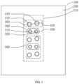
- FIG. 1 a schematic diagram of a printed circuit board according to an embodiment of the present disclosure is shown.
- the printed circuit board 100 includes a substrate 200 and differential signal via pairs 300 and first connecting via groups 400 arranged in the substrate 200.
- the substrate 200 is a substrate with one or more layers, the differential signal via pairs 300 and the first connecting via groups 400 at least partially run through the substrate, and a connecting footprint 210 is arranged on the substrate 200.
- the connecting footprint 210 is provided with at least two differential signal via pairs 300, and the embodiment in FIG. 1 takes two differential signal via pairs 300 as an example.
- the differential signal via pair 300 includes a first signal via 310 and a second signal via 320, and the two differential signal via pairs 300 form a 2 ⁇ 2 signal via matrix.
- the connecting footprint 210 is further provided with at least two first connecting via groups 400, and the embodiment of FIG. 1 takes three first connecting via groups 400 as an example.
- the three first connecting via groups 400 and the two differential signal via pairs 300 are spaced from each other.
- the first connecting via group 400 includes a first connecting via 410 and a second connecting via 420.
- a connecting line between the first signal via 310 and the second signal via 320 in each differential signal via pair 300 forms an acute angle with a connecting line between the first connecting via 410 and the second connecting via 420 in each first connecting via group 400.
- a first connecting line 350 between the first signal via 310 and the second signal via 320 forms an acute angle with a second connecting line 450 between the first connecting via 410 and the second connecting via 420 in each first connecting via group 400.
- the first connecting via groups 400 and the differential signal via pairs 300 are spaced from each other and the connecting line between the signal vias of the differential signal via pair 300 forms an acute angle with the connecting line between the ground vias of the first connecting via group 400, the first connecting via groups 400 are inclined relative to the differential signal via pairs 300, and routing areas therebetween are wide on one side and narrow on the other side. Consequently, differential outgoing lines from the ground vias can be arranged on the wide side, and the large outgoing line space at the wide side also makes it easier to ensure the symmetry of the two signal paths, keep differential tight coupling and help achieve equal-length routing, thus better controlling skew.
- first connecting via groups 400 may be used as ground vias or press-fit vias for a connector.
- first connecting via 410 and the second connecting via 420 are staggered from each other, the first connecting via 410 and the second connecting via 420 can be arranged farther apart, which brings greater convenience for the design of the electrical connector without causing the space occupied by the connecting footprint 210 to become larger.
- the differential signal via pair 300 and adjacent first connecting via groups 400 on both sides thereof form a signal via group 500.
- the connecting footprint 210 includes a plurality of signal via groups 500, and two adjacent signal via groups 500 share one first connecting via group 400.
- the first connecting via groups 400 on both sides of the differential signal via pair 300 surround the differential signal via pair 300 to provide electrical shielding, so as to ensure that signals of the differential signal via pair 300 are free from interference. Since two adjacent signal via groups 500 share one first connecting via group 400, unnecessary space occupation caused by the arrangement of too many first connecting via groups 400 is avoided, ensuring the utilization rate of the space of the printed circuit board 100.
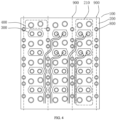
- a plurality of connecting footprints 210 are arranged on the substrate 200, and the differential signal via pairs 300 in two adjacent connecting footprints 210 are arranged in correspondence.
- a plurality of differential signal via pairs 300 are horizontally aligned to form signal via rows 600
- a plurality of first connecting via groups 400 are horizontally aligned to form connecting via rows 700.
- the printed circuit board 100 is further provided with a plurality of third connecting vias 800, which are arranged into second connecting via groups 900, and the second connecting via groups 900 are arranged on both sides of each connecting footprint 210.
- the third connecting vias 800 may be used as both ground vias and press-fit vias for the connector. If the third connecting vias 800 are used as ground vias, the second connecting via groups 900 are arranged on both sides of the connecting footprint 210 to shield signal interference between two adjacent connecting footprints 210. If the third connecting vias 800 are used as press-fit vias for the connector, a better shielding effect can be provided for the connector, thereby ameliorating crosstalks between different columns and eliminating crosstalk resonance between diagonal signal pairs.
- Two adjacent connecting footprints 210 share a same second connecting via group 900.
- Such an arrangement eliminates an excessive provision of the second connecting via groups 900 in the substrate 200, thereby avoiding a waste of the space of the substrate 200.
- a fourth connecting via 430 is arranged between the first connecting via 410 and the second connecting via 420 in each first connecting via group 400, which can further improve the electrical shielding effect of the first connecting via group 400.
- the size of the fourth connecting via 430 may be set as needed. For example, if the space between the first connecting via 410 and the second connecting via 420 is small, the fourth connecting via 430 may be set to be small.
- the acute angle formed by the connecting line between the signal vias of the differential signal via pair 300 and the connecting line between the ground vias of the first connecting via group 400 is greater than 0 degrees and less than 45 degrees.
- limiting the acute angle to be greater than 0 degrees and less than 45 degrees can not only meet the requirement of providing a space for the outgoing lines, but also ensure the utilization rate of the space of the printed circuit board 100.
- the printed circuit board 100 further includes signal traces 330 electrically connected to the differential signal via pairs 300, a routing area 340 is formed between the differential signal via pair 300 and the first connecting via group 400 which are adjacent, and the signal traces 330 extend from the routing area 340 to the differential signal via pair 300.
- the first connecting via group 400 is inclined relative to the differential signal via pair 300, so that the routing area 340 therebetween is wide on one side and narrow on the other side.
- the routing area 340 in FIG. 5 is approximately trapezoidal, or may also be considered to be approximately triangular. It can be understood that the signal traces 330 extend from the wide side of the routing area 340 to the differential signal via pair 300, which makes it easier to ensure the symmetry of the two signal paths and help achieve equal-length routing, thus better controlling skew.
- the signal traces 330 extend from between two adjacent connecting footprints 210 to the edge of the substrate 200.
- the signal trace 330 may be completely included in one connecting footprint 210; or may be partially included in one connecting footprint 210 and partially included in an adjacent connecting footprint 210; or when there is a gap or space between two adjacent connecting footprints 210, may be arranged in the gap or space.
- the second connecting via group 900 may be arranged between multiple groups of signal traces 330 to shield interference between the signal traces 330.
- an embodiment further provides an electronic device, including the printed circuit board described in the above embodiments.
- the device includes, but not limited to, a communication device requiring high-speed transmission, such as a router, a data storage unit, a server, a mobile phone, a tablet or a cellphone.
- a printed circuit board of the communication device is connected to an electrical connector through the connecting footprints 210, so as to implement high-speed data transmission with other electronic devices.
- the first connecting via groups and the differential signal via pairs are spaced from each other and the connecting line between the signal vias of the differential signal via pair forms an acute angle with the connecting line between the ground vias of the first connecting via group, the first connecting via groups are inclined relative to the differential signal via pairs, such that routing areas therebetween are wide on one side and narrow on the other side. Consequently, differential outgoing lines from the ground vias can be arranged on the wide side, and the large outgoing line space also makes it easier to ensure the symmetry of the two signal paths and help achieve equal-length routing, thus better controlling skew.
Landscapes
- Engineering & Computer Science (AREA)
- Microelectronics & Electronic Packaging (AREA)
- Physics & Mathematics (AREA)
- Electromagnetism (AREA)
- Structure Of Printed Boards (AREA)
Applications Claiming Priority (2)
| Application Number | Priority Date | Filing Date | Title |
|---|---|---|---|
| CN202010595816.9A CN113840451A (zh) | 2020-06-24 | 2020-06-24 | 印刷电路板及具有该印刷电路板的电子设备 |
| PCT/CN2021/097790 WO2021259021A1 (fr) | 2020-06-24 | 2021-06-01 | Carte de circuit imprimé et dispositif électronique doté de la carte de circuit imprimé |
Publications (2)
| Publication Number | Publication Date |
|---|---|
| EP4171179A1 true EP4171179A1 (fr) | 2023-04-26 |
| EP4171179A4 EP4171179A4 (fr) | 2023-12-20 |
Family
ID=78965025
Family Applications (1)
| Application Number | Title | Priority Date | Filing Date |
|---|---|---|---|
| EP21829849.5A Pending EP4171179A4 (fr) | 2020-06-24 | 2021-06-01 | Carte de circuit imprimé et dispositif électronique doté de la carte de circuit imprimé |
Country Status (5)
| Country | Link |
|---|---|
| EP (1) | EP4171179A4 (fr) |
| JP (1) | JP7482265B2 (fr) |
| KR (1) | KR102865157B1 (fr) |
| CN (1) | CN113840451A (fr) |
| WO (1) | WO2021259021A1 (fr) |
Families Citing this family (4)
| Publication number | Priority date | Publication date | Assignee | Title |
|---|---|---|---|---|
| CN114566842B (zh) * | 2022-04-29 | 2022-07-26 | 苏州浪潮智能科技有限公司 | 信号转接装置及信号传输系统 |
| CN115119401B (zh) * | 2022-07-28 | 2024-01-19 | 苏州浪潮智能科技有限公司 | 一种印刷电路板及电子设备 |
| CN115864038B (zh) * | 2023-02-24 | 2023-05-02 | 深圳市西点精工技术有限公司 | 一种具有抗短桩效应的高速背板连接器 |
| CN118945982A (zh) * | 2024-07-22 | 2024-11-12 | 中航光电科技股份有限公司 | 一种电路板、连接器及连接器组件 |
Family Cites Families (6)
| Publication number | Priority date | Publication date | Assignee | Title |
|---|---|---|---|---|
| US7108556B2 (en) * | 2004-07-01 | 2006-09-19 | Amphenol Corporation | Midplane especially applicable to an orthogonal architecture electronic system |
| US8251745B2 (en) * | 2007-11-07 | 2012-08-28 | Fci Americas Technology Llc | Electrical connector system with orthogonal contact tails |
| US9930772B2 (en) * | 2015-12-30 | 2018-03-27 | Te Connectivity Corporation | Printed circuit and circuit board assembly configured for quad signaling |
| US9923309B1 (en) * | 2017-01-27 | 2018-03-20 | Te Connectivity Corporation | PCB connector footprint |
| US10559929B2 (en) * | 2018-01-25 | 2020-02-11 | Te Connectivity Corporation | Electrical connector system having a PCB connector footprint |
| CN110730558B (zh) * | 2019-09-09 | 2021-02-12 | 华为机器有限公司 | 印刷电路板及通信设备 |
-
2020
- 2020-06-24 CN CN202010595816.9A patent/CN113840451A/zh active Pending
-
2021
- 2021-06-01 JP JP2022579877A patent/JP7482265B2/ja active Active
- 2021-06-01 EP EP21829849.5A patent/EP4171179A4/fr active Pending
- 2021-06-01 WO PCT/CN2021/097790 patent/WO2021259021A1/fr not_active Ceased
- 2021-06-01 KR KR1020227044959A patent/KR102865157B1/ko active Active
Also Published As
| Publication number | Publication date |
|---|---|
| CN113840451A (zh) | 2021-12-24 |
| WO2021259021A1 (fr) | 2021-12-30 |
| KR20230015417A (ko) | 2023-01-31 |
| JP2023532260A (ja) | 2023-07-27 |
| EP4171179A4 (fr) | 2023-12-20 |
| KR102865157B1 (ko) | 2025-09-29 |
| JP7482265B2 (ja) | 2024-05-13 |
Similar Documents
| Publication | Publication Date | Title |
|---|---|---|
| EP4171179A1 (fr) | Carte de circuit imprimé et dispositif électronique doté de la carte de circuit imprimé | |
| US10194524B1 (en) | Anti-pad for signal and power vias in printed circuit board | |
| US8080738B2 (en) | Printed circuit having ground vias between signal vias | |
| US20060073709A1 (en) | High density midplane | |
| US10791629B1 (en) | Printed circuit board configuration to facilitate a surface mount double density QSFP connector footprint in a belly-to-belly alignment | |
| KR102875208B1 (ko) | 인쇄 회로 기판, 백플레인 아키텍처 시스템 및 통신 디바이스 | |
| US20110007487A1 (en) | Lsi package, printed board and electronic device | |
| CN101159559B (zh) | 一种背板及实现方法 | |
| WO2023273757A1 (fr) | Carte de circuit imprimé et dispositif électronique | |
| CN113690649B (zh) | 一种连接器组件 | |
| CN104752851B (zh) | 一种系统 | |
| JP2024533681A (ja) | プリント回路基板及び信号伝送システム | |
| US20260013050A1 (en) | Wave soldering device, manufacturing method thereof and printed circuit board | |
| US20080025007A1 (en) | Partially plated through-holes and achieving high connectivity in multilayer circuit boards using the same | |
| CN120857344A (zh) | 差分过孔结构、焊球阵列封装组件、印刷电路板及通信设备 | |
| US8044305B2 (en) | Circuit board including hybrid via structures | |
| CN210804234U (zh) | 背板以及电子终端 | |
| US20250386426A1 (en) | Electronic circuit board | |
| CN221178001U (zh) | 电路板及电子设备 | |
| US20250306314A1 (en) | Maintaining signal integrity for high data rate optical connectors | |
| CN114567968B (zh) | 一种能提高asaac背板si性能的背板布线结构及布线方法 | |
| CN114122831B (zh) | 一种连接器组件和通信设备 | |
| KR100505641B1 (ko) | 메모리 모듈 및 이를 구비하는 메모리 시스템 | |
| US20250331103A1 (en) | Circuit board and electronic device | |
| CN121568298B (zh) | 电路板和电子设备 |
Legal Events
| Date | Code | Title | Description |
|---|---|---|---|
| STAA | Information on the status of an ep patent application or granted ep patent |
Free format text: STATUS: THE INTERNATIONAL PUBLICATION HAS BEEN MADE |
|
| PUAI | Public reference made under article 153(3) epc to a published international application that has entered the european phase |
Free format text: ORIGINAL CODE: 0009012 |
|
| STAA | Information on the status of an ep patent application or granted ep patent |
Free format text: STATUS: REQUEST FOR EXAMINATION WAS MADE |
|
| 17P | Request for examination filed |
Effective date: 20230123 |
|
| AK | Designated contracting states |
Kind code of ref document: A1 Designated state(s): AL AT BE BG CH CY CZ DE DK EE ES FI FR GB GR HR HU IE IS IT LI LT LU LV MC MK MT NL NO PL PT RO RS SE SI SK SM TR |
|
| DAV | Request for validation of the european patent (deleted) | ||
| DAX | Request for extension of the european patent (deleted) | ||
| REG | Reference to a national code |
Ref country code: DE Ref legal event code: R079 Free format text: PREVIOUS MAIN CLASS: H05K0001110000 Ipc: H05K0001020000 |
|
| A4 | Supplementary search report drawn up and despatched |
Effective date: 20231120 |
|
| RIC1 | Information provided on ipc code assigned before grant |
Ipc: H05K 1/11 20060101ALN20231114BHEP Ipc: H05K 1/02 20060101AFI20231114BHEP |