EP4173824A1 - Composition de photorésine, système comprenant une composition de photorésine, procédé de fabrication d'une structure tridimensionnelle, et utilisation d'une composition de photorésine dans l'impression 3d - Google Patents
Composition de photorésine, système comprenant une composition de photorésine, procédé de fabrication d'une structure tridimensionnelle, et utilisation d'une composition de photorésine dans l'impression 3d Download PDFInfo
- Publication number
- EP4173824A1 EP4173824A1 EP21205242.7A EP21205242A EP4173824A1 EP 4173824 A1 EP4173824 A1 EP 4173824A1 EP 21205242 A EP21205242 A EP 21205242A EP 4173824 A1 EP4173824 A1 EP 4173824A1
- Authority
- EP
- European Patent Office
- Prior art keywords
- photoresist composition
- state
- polymerization
- photoinitiator
- continuous
- Prior art date
- Legal status (The legal status is an assumption and is not a legal conclusion. Google has not performed a legal analysis and makes no representation as to the accuracy of the status listed.)
- Pending
Links
Images






Classifications
-
- G—PHYSICS
- G03—PHOTOGRAPHY; CINEMATOGRAPHY; ANALOGOUS TECHNIQUES USING WAVES OTHER THAN OPTICAL WAVES; ELECTROGRAPHY; HOLOGRAPHY
- G03F—PHOTOMECHANICAL PRODUCTION OF TEXTURED OR PATTERNED SURFACES, e.g. FOR PRINTING, FOR PROCESSING OF SEMICONDUCTOR DEVICES; MATERIALS THEREFOR; ORIGINALS THEREFOR; APPARATUS SPECIALLY ADAPTED THEREFOR
- G03F7/00—Photomechanical, e.g. photolithographic, production of textured or patterned surfaces, e.g. printing surfaces; Materials therefor, e.g. comprising photoresists; Apparatus specially adapted therefor
- G03F7/0037—Production of three-dimensional images
-
- B—PERFORMING OPERATIONS; TRANSPORTING
- B29—WORKING OF PLASTICS; WORKING OF SUBSTANCES IN A PLASTIC STATE IN GENERAL
- B29C—SHAPING OR JOINING OF PLASTICS; SHAPING OF MATERIAL IN A PLASTIC STATE, NOT OTHERWISE PROVIDED FOR; AFTER-TREATMENT OF THE SHAPED PRODUCTS, e.g. REPAIRING
- B29C64/00—Additive manufacturing, i.e. manufacturing of three-dimensional [3D] objects by additive deposition, additive agglomeration or additive layering, e.g. by 3D printing, stereolithography or selective laser sintering
- B29C64/10—Processes of additive manufacturing
- B29C64/106—Processes of additive manufacturing using only liquids or viscous materials, e.g. depositing a continuous bead of viscous material
- B29C64/124—Processes of additive manufacturing using only liquids or viscous materials, e.g. depositing a continuous bead of viscous material using layers of liquid which are selectively solidified
- B29C64/129—Processes of additive manufacturing using only liquids or viscous materials, e.g. depositing a continuous bead of viscous material using layers of liquid which are selectively solidified characterised by the energy source therefor, e.g. by global irradiation combined with a mask
- B29C64/135—Processes of additive manufacturing using only liquids or viscous materials, e.g. depositing a continuous bead of viscous material using layers of liquid which are selectively solidified characterised by the energy source therefor, e.g. by global irradiation combined with a mask the energy source being concentrated, e.g. scanning lasers or focused light sources
-
- B—PERFORMING OPERATIONS; TRANSPORTING
- B29—WORKING OF PLASTICS; WORKING OF SUBSTANCES IN A PLASTIC STATE IN GENERAL
- B29C—SHAPING OR JOINING OF PLASTICS; SHAPING OF MATERIAL IN A PLASTIC STATE, NOT OTHERWISE PROVIDED FOR; AFTER-TREATMENT OF THE SHAPED PRODUCTS, e.g. REPAIRING
- B29C64/00—Additive manufacturing, i.e. manufacturing of three-dimensional [3D] objects by additive deposition, additive agglomeration or additive layering, e.g. by 3D printing, stereolithography or selective laser sintering
- B29C64/20—Apparatus for additive manufacturing; Details thereof or accessories therefor
- B29C64/264—Arrangements for irradiation
- B29C64/268—Arrangements for irradiation using laser beams; using electron beams [EB]
-
- B—PERFORMING OPERATIONS; TRANSPORTING
- B33—ADDITIVE MANUFACTURING TECHNOLOGY
- B33Y—ADDITIVE MANUFACTURING, i.e. MANUFACTURING OF THREE-DIMENSIONAL [3D] OBJECTS BY ADDITIVE DEPOSITION, ADDITIVE AGGLOMERATION OR ADDITIVE LAYERING, e.g. BY 3D PRINTING, STEREOLITHOGRAPHY OR SELECTIVE LASER SINTERING
- B33Y10/00—Processes of additive manufacturing
-
- B—PERFORMING OPERATIONS; TRANSPORTING
- B33—ADDITIVE MANUFACTURING TECHNOLOGY
- B33Y—ADDITIVE MANUFACTURING, i.e. MANUFACTURING OF THREE-DIMENSIONAL [3D] OBJECTS BY ADDITIVE DEPOSITION, ADDITIVE AGGLOMERATION OR ADDITIVE LAYERING, e.g. BY 3D PRINTING, STEREOLITHOGRAPHY OR SELECTIVE LASER SINTERING
- B33Y30/00—Apparatus for additive manufacturing; Details thereof or accessories therefor
-
- B—PERFORMING OPERATIONS; TRANSPORTING
- B33—ADDITIVE MANUFACTURING TECHNOLOGY
- B33Y—ADDITIVE MANUFACTURING, i.e. MANUFACTURING OF THREE-DIMENSIONAL [3D] OBJECTS BY ADDITIVE DEPOSITION, ADDITIVE AGGLOMERATION OR ADDITIVE LAYERING, e.g. BY 3D PRINTING, STEREOLITHOGRAPHY OR SELECTIVE LASER SINTERING
- B33Y70/00—Materials specially adapted for additive manufacturing
-
- G—PHYSICS
- G03—PHOTOGRAPHY; CINEMATOGRAPHY; ANALOGOUS TECHNIQUES USING WAVES OTHER THAN OPTICAL WAVES; ELECTROGRAPHY; HOLOGRAPHY
- G03F—PHOTOMECHANICAL PRODUCTION OF TEXTURED OR PATTERNED SURFACES, e.g. FOR PRINTING, FOR PROCESSING OF SEMICONDUCTOR DEVICES; MATERIALS THEREFOR; ORIGINALS THEREFOR; APPARATUS SPECIALLY ADAPTED THEREFOR
- G03F7/00—Photomechanical, e.g. photolithographic, production of textured or patterned surfaces, e.g. printing surfaces; Materials therefor, e.g. comprising photoresists; Apparatus specially adapted therefor
- G03F7/004—Photosensitive materials
- G03F7/027—Non-macromolecular photopolymerisable compounds having carbon-to-carbon double bonds, e.g. ethylenic compounds
- G03F7/028—Non-macromolecular photopolymerisable compounds having carbon-to-carbon double bonds, e.g. ethylenic compounds with photosensitivity-increasing substances, e.g. photoinitiators
- G03F7/029—Inorganic compounds; Onium compounds; Organic compounds having hetero atoms other than oxygen, nitrogen or sulfur
-
- G—PHYSICS
- G03—PHOTOGRAPHY; CINEMATOGRAPHY; ANALOGOUS TECHNIQUES USING WAVES OTHER THAN OPTICAL WAVES; ELECTROGRAPHY; HOLOGRAPHY
- G03F—PHOTOMECHANICAL PRODUCTION OF TEXTURED OR PATTERNED SURFACES, e.g. FOR PRINTING, FOR PROCESSING OF SEMICONDUCTOR DEVICES; MATERIALS THEREFOR; ORIGINALS THEREFOR; APPARATUS SPECIALLY ADAPTED THEREFOR
- G03F7/00—Photomechanical, e.g. photolithographic, production of textured or patterned surfaces, e.g. printing surfaces; Materials therefor, e.g. comprising photoresists; Apparatus specially adapted therefor
- G03F7/004—Photosensitive materials
- G03F7/027—Non-macromolecular photopolymerisable compounds having carbon-to-carbon double bonds, e.g. ethylenic compounds
- G03F7/028—Non-macromolecular photopolymerisable compounds having carbon-to-carbon double bonds, e.g. ethylenic compounds with photosensitivity-increasing substances, e.g. photoinitiators
- G03F7/031—Organic compounds not covered by group G03F7/029
-
- G—PHYSICS
- G03—PHOTOGRAPHY; CINEMATOGRAPHY; ANALOGOUS TECHNIQUES USING WAVES OTHER THAN OPTICAL WAVES; ELECTROGRAPHY; HOLOGRAPHY
- G03F—PHOTOMECHANICAL PRODUCTION OF TEXTURED OR PATTERNED SURFACES, e.g. FOR PRINTING, FOR PROCESSING OF SEMICONDUCTOR DEVICES; MATERIALS THEREFOR; ORIGINALS THEREFOR; APPARATUS SPECIALLY ADAPTED THEREFOR
- G03F7/00—Photomechanical, e.g. photolithographic, production of textured or patterned surfaces, e.g. printing surfaces; Materials therefor, e.g. comprising photoresists; Apparatus specially adapted therefor
- G03F7/20—Exposure; Apparatus therefor
- G03F7/2051—Exposure without an original mask, e.g. using a programmed deflection of a point source, by scanning, by drawing with a light beam, using an addressed light or corpuscular source
- G03F7/2053—Exposure without an original mask, e.g. using a programmed deflection of a point source, by scanning, by drawing with a light beam, using an addressed light or corpuscular source using a laser
-
- B—PERFORMING OPERATIONS; TRANSPORTING
- B29—WORKING OF PLASTICS; WORKING OF SUBSTANCES IN A PLASTIC STATE IN GENERAL
- B29K—INDEXING SCHEME ASSOCIATED WITH SUBCLASSES B29B, B29C OR B29D, RELATING TO MOULDING MATERIALS OR TO MATERIALS FOR MOULDS, REINFORCEMENTS, FILLERS OR PREFORMED PARTS, e.g. INSERTS
- B29K2033/00—Use of polymers of unsaturated acids or derivatives thereof as moulding material
- B29K2033/04—Polymers of esters
-
- B—PERFORMING OPERATIONS; TRANSPORTING
- B29—WORKING OF PLASTICS; WORKING OF SUBSTANCES IN A PLASTIC STATE IN GENERAL
- B29K—INDEXING SCHEME ASSOCIATED WITH SUBCLASSES B29B, B29C OR B29D, RELATING TO MOULDING MATERIALS OR TO MATERIALS FOR MOULDS, REINFORCEMENTS, FILLERS OR PREFORMED PARTS, e.g. INSERTS
- B29K2105/00—Condition, form or state of moulded material or of the material to be shaped
- B29K2105/0002—Condition, form or state of moulded material or of the material to be shaped monomers or prepolymers
-
- B—PERFORMING OPERATIONS; TRANSPORTING
- B29—WORKING OF PLASTICS; WORKING OF SUBSTANCES IN A PLASTIC STATE IN GENERAL
- B29K—INDEXING SCHEME ASSOCIATED WITH SUBCLASSES B29B, B29C OR B29D, RELATING TO MOULDING MATERIALS OR TO MATERIALS FOR MOULDS, REINFORCEMENTS, FILLERS OR PREFORMED PARTS, e.g. INSERTS
- B29K2105/00—Condition, form or state of moulded material or of the material to be shaped
- B29K2105/0005—Condition, form or state of moulded material or of the material to be shaped containing compounding ingredients
Definitions
- the present invention relates to a photoresist composition, a system, in particular for 3D-printing, comprising a photoresist composition, a method for producing a three-dimensional structure, and a use of a photoresist composition in 3D-printing.
- a two-photon absorption process illustrated in Fig. 1 the light field induces a state in between the ground state and a relevant excited state of a quantum system, e.g., a molecule.
- This induced state (see dashed line in Fig. 1a ), or dressed state in the language of quantum optics, is commonly referred to as a virtual state.
- This state really exists, but only as long as the light field is switched on.
- the virtual state lifetime is determined by the pulse duration.
- a first photon induces the transition of an electron from the ground state to the virtual state, from which a second photon induces the transition to the excited state.
- Multiphoton optical lithography has become a well-established method to fabricate three-dimensional (3D) structures from the nano- to the microscale.
- 3D optical lithography aka direct laser writing or 3D laser nanoprinting
- two-photon absorption leads to a scaling of the photoinitiator transition rate and hence of the exposure dose proportional to l 2 , i.e., the light intensity squared.
- this quadratic nonlinearity suppresses unavoidable lateral and axial tails of the diffraction-limited laser focus and thereby warrants the crucial concentration of the excitation and the following chemical reaction along all three spatial directions.
- one-photon absorption alone without additional nonlinearities fundamentally cannot provide this concentration in the making of arbitrary 3D structures.
- mode-locked pico- or femtosecond laser sources are routinely used.
- micro-explosions occur due to the onset of three- and four-photon absorption processes and beyond, leading to the unwanted population of high-energy electron states.
- the laser power at which micro-explosions occur is less than an order of magnitude above the writing point.
- the process window is even as small as 10%. Small pollutions or dirt microparticles in the photoresist can trigger micro-explosions even at the writing point. Such events render entire time-consuming 3D-printing jobs useless.
- a problem to be solved by the present invention is to improve 3D-printing.
- An aspect of the present invention relates to a photoresist composition, comprising:
- the above-mentioned photoresist composition contributes to miniaturization of 3D-microprinting and 3D-nanoprinting devices, herein also referred to as 3D-printing devices, and renders 3D-printing more cost-efficient.
- the photoresist composition enables more efficient 3D-printing while maintaining high printing resolution.
- three-dimensional micro- and/or nanostructures may be printed, being extendable to large scale structures.
- polymerizable monomer is not particularly restricted and may include one type of polymerizable monomer or may include a mixture of two or more polymerizable monomers.
- type of polymerization monomer is not limited and may, for example, include monomers suitable for radical polymerization, cationic or anionic polymerization, as well as monomers following specific polymerization mechanisms such as thiol-ene-based or thiol-yne-based polymerization, or Diels-Alder cycloaddition.
- polymerizable monomers examples include acrylates, methacrylates, acrylamides, methacrylamides, styrenes and other vinyl compounds, alkenes including dienes, alkynes, lactones, lactams, (cyclic) amines, and thiols.
- photoinitiator used herein is not particularly restricted and includes such compounds which create reactive species such as radicals, cations or anions upon irradiation with light, for example of the UV, VIS or IR wavelength range. These reactive species are then capable of initiating and/or promoting polymerization of the polymerizable monomer.
- polymerization inhibitor is not particularly restricted and used in a general sense to describe any compound capable of preventing unwanted polymerization.
- polymerization inhibitor as used herein includes both retarders and true inhibitors. This may also include singlet or triplet state quenchers.
- quantum mechanical energy states or quantum states normally refer to a set of quantum numbers, such as energy level number and spin, which describe the dynamics of electrons in a quantum system such as an atom or a molecule.
- Quantum states mathematically refer to wavefunctions which are determined as solutions of the Schrödinger equation of an atom or a molecule.
- the electronic quantum states may, in the framework of this description, be single-particle states or wavefunctions of the electrons of an atom or a molecule.
- These single-particle states may be solutions of the Schrödinger equation for the electrons of an atom or a molecule using a mean-field approximation of the electrostatic interactions of the electrons as, for example, in the so-called Hartree-Fock approach or density functional theory.
- the single-particle states of the electrons obtained in such a way may be atomic orbitals or molecular orbitals.
- ground state refers to the energetically highest single-particle state, i.e., atomic or molecular orbital, that an electron of the photoinitiator may have or - in quantum chemistry language - occupy below or at room temperature.
- intermediate state refers to an orbital which is higher in energy than the ground state.
- polymerization-inducing state refers to an orbital higher in energy than the intermediate state, which when occupied by an electron by excitation of the electron from the ground state or intermediate state induces the polymerization of the polymerizable monomers in the photoresist composition.
- optically excitable state refers to an electronic quantum state or orbital which may be reached or occupied by light excitations, i.e., by electron-photon interactions, such as electron-photon scattering processes.
- An electron may be excited by being hit by a photon and/or absorbing the photon of a specific wavelength and/or frequency corresponding to the excitation energy from the previous state to the optically excitable state.
- substantially optically excitable state refers to the situation that a state to be excited may be occupied only by an optical excitation by an electron-photon hit and/or exciting an electron by absorbing a photon, or the state to be excited may be occupied by an optical excitation of an electron to a metastable state from which the electron may then relax to the state to be excited.
- the term "lifetime” means the time until an electron relaxes from a state to an energetically lower state or the time after which a state is de-occupied by an electron.
- the relaxation process or de-occupying process may be a radiation-free process or may occur by radiation. That is, an electron may emit a photon of an energy corresponding to the energy difference between the metastable state and the state to be excited when relaxing from the metastable state to the state to be excited.
- the lifetime may be about 80 ⁇ s.
- the lifetime may also be in the range of about 1 ⁇ s to about 10 ms.
- the lifetime of the first intermediate state is long enough so that the first intermediate state can be populated using low optical powers, simultaneously, short enough so that after an exposure, the photoinitiator molecules outside the focal region quickly return to their ground state and subsequent focal regions may be exposed in rapid succession, as described further below in more detail. More generally, it is advantageous that the amount of photoinitiator molecules excited to the first intermediate state always stays small compared to the amount of photoinitiator molecules in the ground state, i.e., it is advantageous that there is no population inversion.
- single-photon excitation refers to excitations which are caused by hitting an electron by one single photon and/or absorbing the photon by the electron.
- the photon needs to have a specific wavelength and/or frequency corresponding to the excitation energy of the electron, i.e., the energy difference between an initial state and the state to be excited.
- the polymerization-inducing state may be optically excitable by at least two sequential single-photon excitations of substantially the same predetermined wavelength.
- the photoresist composition provides a comparable nonlinear transition rate scaling regarding the intensity / from the ground state to the polymerization-inducing state of / 2 as in the case of two-photon absorption-based 3D-printing.
- the photoresist composition enables 3D-printing at high resolution and/or high printing velocity.
- the spatial localization of optical excitations may be increased, whereby the resolution of 3D-printing may be improved.
- the wavelengths of the two subsequent photons causing the sequential two single-photon excitations may absolutely differ by about 0%, by utmost about 1%, by utmost about 5%, by utmost about 10%, or by utmost about 20%. However, in principle, it is also possible that the wavelengths of the two subsequent photons causing the sequential two single-photon excitations differ by more than about 20%.
- the two sequential single-photon excitations may herein also be referred to as two-step absorption.
- Three sequential single-photon excitations may be referred to as three-step absorption.
- Four sequential single-photon excitations may be referred to as four-step photon absorption, and so on.
- the predetermined wavelength may be at least about 300 nm and/or utmost about 900 nm.
- the predetermined wavelength may also be at least about 400 nm and/or utmost about 800 nm.
- the predetermined wavelength may be about 405 nm, about 440 nm, about 488 nm, about 532 nm, or about 640 nm.
- the single-photon excitation may have a predetermined frequency of at least about 0.3 PHz and/or utmost about 1 PHz.
- the single-photon excitation may also have a frequency of at least about 0.375 PHz and/or utmost about 0.75 PHz.
- the frequency may be about 0.74 PHz, about 0.68 PHz, about 0.61 PHz, about 0.56 PHz, or about 0.47 PHz.
- the single-photon excitation may be of at least about 1.24 eV and/or utmost about 4.14 eV.
- the single-photon excitation may also be of at least about 1.55 eV and/or utmost about 3.11 eV.
- the single-photon excitation may be of about 3.07 eV, about 2.82 eV, about 2.53 eV, about 2.32 eV, or about 1.95 eV.
- the wavelength may be the wavelength of the light emitted by a laser used in a Blu-ray player, a DVD player, a Blu-ray writing device, a DVD writing device, or a laser pointer.
- the first intermediate state may be a real state.
- the first intermediate state may be a relaxed state with respect to an energetically higher state being optically excitable from the ground state by a single-photon excitation of the predetermined wavelength.
- the first intermediate state may be a state which is reachable by an intersystem crossing of the photoinitiator.
- the first intermediate state may be a state of different orientation of total spin or spin multiplicity than the energetically higher state.
- the first intermediate state may, for example, be a triplet state, whereas the energetically higher state may be a singlet state.
- the photoinitiator may comprise multiple intermediate states as described above. All features described with respect to the first intermediate state apply to each of the multiple intermediate states.
- the photoinitiator may have a second intermediate state energetically lower than the first intermediate state and lower than the polymerization-inducing state, wherein the second intermediate state may be substantially optically excitable from the ground state, and wherein the first intermediate state may be optically excitable from the second intermediate state based on a single-photon excitation of substantially the predetermined frequency.
- the photoinitiator may have a third intermediate state energetically lower than the second intermediate state and lower than the polymerization-inducing state, wherein the third intermediate state may be substantially optically excitable from the ground state, and wherein the second intermediate state may be optically excitable from the third intermediate state based on a single-photon excitation of substantially the predetermined frequency, and so on.
- the photoinitiator may have a linear, molar extinction coefficient in the ground state of about 0.1 to about 1000 M -1 cm -1 at the predetermined wavelength.
- the photoinitiator may have a linear, molar extinction coefficient in the ground state of about 50 M -1 cm -1 at the predetermined wavelength.
- the photoinitiator may have a linear, molar extinction coefficient in at least one of the multiple intermediate states of about 10 to about 100 000 M -1 cm -1 at the predetermined wavelength.
- the photoinitiator may have a linear, molar extinction coefficient in at least one of the multiple intermediate states of about 5000 M -1 cm -1 at the predetermined wavelength.
- the multiple intermediate states may have an energy of utmost about 70 kcal/mol.
- the multiple intermediate states may have an energy of utmost about 60 kcal/mol.
- At least one of the multiple intermediate states may be inert.
- the photoinitiator may be selected from the group consisting of alpha-diketones such as benzil, beta-diketones, gamma-diketones, spiropyrans, merocyanines, carbazoles, thiophenes, polycyclic aromatic hydrocarbons, triketones, photoenoles, (di-)acylgermanes, bis(germyl)ketones, and thioxanthones.
- alpha-diketones such as benzil, beta-diketones, gamma-diketones, spiropyrans, merocyanines, carbazoles, thiophenes, polycyclic aromatic hydrocarbons, triketones, photoenoles, (di-)acylgermanes, bis(germyl)ketones, and thioxanthones.
- the polymerization inhibitor may be selected from the group consisting of 2,2,6,6-tetramethyl-4-piperidyl-1-oxyl (TEMPO) and derivatives thereof, bis(2,2,6,6-tetramethyl-4-piperidyl-1-oxyl) sebacate (BTPOS) and derivatives thereof, other hindered amine light stabilizers (HALS), 1,4-diazabicyclo[2.2.2]octane (DABCO), n-propyl gallate (NPG), p-phenylenediamine (PPD), cyclodextrines, phenothiazines, hydroxylamines, quinones, mequinol, 4-tert-butylcatechol (TBC), butylated hydroxytoluene (BHT), nitrobenzenes, phenol, p-nitrophenol, stilbenes, galvinoxyl, and azulene.
- HALS hindered amine light stabilizers
- DABCO 1,4-diazabicyclo
- the content of the photoinitiator may be 0.1% to 10% by weight based on the photoresist composition. Additionally or alternatively, the content of the polymerization inhibitor may be 0.05% to 10% by weight based on the photoresist composition.
- the photoinitiator may have a plurality of absorption bands at at least about 300 nm and utmost about 900 nm.
- the photoinitiator may have a plurality of absorption bands at at least about 400 nm and utmost about 800 nm.
- the photoinitiator may have at least one absorption band at about 405 nm and/or about 440 nm and/or about 488 nm and/or about 532 nm and/or about 640 nm.
- the plurality of absorption bands may overlap.
- Another aspect of the present invention relates to a system, in particular for 3D-printing, comprising:
- the aforesaid system allows for cost-efficient and highly accurate 3D-printing, in particular on the scale of micrometers and/or nanometers, being extendable to larger scales. Furthermore, the system may be manufactured in a more compact fashion.
- the at least one continuous-wave light source may comprise a laser and/or a light emitting diode.
- the at least one continuous-wave light source may be a laser and/or a light emitting diode.
- the at least one continuous-wave light source may comprise or be a laser used in a Blu-ray player and/or a DVD player and/or a Blu-ray writing device and/or a DVD writing device and/or a laser pointer.
- the at least one continuous-wave light source may also comprise or be any suitable lamp, for example a mercury vapor lamp, a metal-halide lamp, or the like.
- the at least one continuous-wave light source may comprise or be a non-pulsed laser.
- the at least one continuous-wave light source may include quasi continuous-wave light sources which are continuous-wave light sources that may be periodically interrupted.
- the light emitted by the at least one continuous-wave light source may have a wavelength of at least about 300 nm and/or utmost about 900 nm.
- the predetermined wavelength may also be at least about 400 nm and/or utmost about 800 nm.
- the predetermined wavelength may be about 405 nm, about 440 nm, about 488 nm, about 532 nm, or about 640 nm.
- the light emitted by the at least one continuous-wave light source may have a frequency of at least about 0.3 PHz and/or utmost about 1 PHz.
- the light emitted by the at least one continuous-wave light source may also have a frequency of at least about 0.375 PHz and/or utmost about 0.75 PHz.
- the frequency may be about 0.74 PHz, about 0.68 PHz, about 0.61 PHz, about 0.56 PHz, or about 0.47 PHz.
- the at least one continuous-wave light source may have an optical power of about 1 mW or larger.
- the at least one continuous-wave light source may also have an optical power in the range of about 1 mW to about 1 W, e.g., about 100 mW.
- the at least one continuous-wave light source may further have an optical power of about 1 W or larger.
- the optical power of the at least one continuous-wave light source may be at least large enough to trigger the polymerization reaction inside the spatial location of the focus of the emitted light.
- the optical power used for irradiating the photoresist composition in the spatial location of the focus of the emitted light may be about 1 mW or smaller, 100 ⁇ W or smaller, or 50 ⁇ W or smaller, without, however, being limited thereto.
- the at least one continuous-wave light source may include 1, 2, 3, 4, 5, 6, 7, 8, 9 or 10 continuous-wave light sources.
- the system may further comprise a focusing unit for focusing the light emitted by the at least one continuous-wave light source on the photoresist composition.
- the focusing unit focuses the light emitted by the at least one continuous-wave light source and sets a first spatial location of the focus of the emitted light, wherein the first spatial location of the focus corresponds to a volume element of the photoresist composition.
- the focusing unit may comprise one or more of the following: a collimator, a plano-convex lens, a pinhole, a mirror, a polarizer, and an objective lens.
- the system may also further comprise a positioning unit for controlling the position of the focusing unit with respect to the position of the photoresist composition.
- the positioning unit spatially controls the focus of the emitted light such that the focus of the emitted light is movable from the first spatial location to a second spatial location of the focus, wherein the second spatial location of the focus corresponds to a second volume element of the photoresist composition, wherein the first volume element is substantially different from the second volume element.
- Positioning may be accomplished by moving the focusing unit and/or by moving the photoresist composition.
- the focus of the light emitted by the at least one continuous-wave light source refers to a spatial region, also referred to herein as focal region, in which the light intensity and/or light power of the light emitted by the at least one continuous-wave light source is focused or concentrated.
- the focal region may be substantially two-dimensional. It may also be three-dimensional.
- the first volume element and the second volume element may each correspond to the focal region.
- the first volume element and the second volume element may also overlap.
- the positioning unit may comprise a mirror arrangement and/or a stage.
- the stage is where the photoresist composition may be positioned.
- the mirror arrangement may comprise one or more fixed mirrors, and/or one or more motorized mirrors.
- the motorized mirrors may be piezoelectric, galvanometric or MEMS (micro-electro-mechanical systems) actuated mirrors.
- the stage may be motorized and may comprise stepper or servo motors, or piezoelectric, voice coil, or other magnetic actuators.
- the positioning unit may comprise fixed and/or motorized mirrors, and/or a fixed and/or motorized stage.
- the system may be a confocal microscope.
- Yet another aspect of the present invention relates to a method for producing a three-dimensional structure, wherein the method comprises the following steps:
- a three-dimensional structure in particular on the micro- and/or nanoscale, being extendable to larger scales, may be produced or manufactured with high resolution and in a cost-efficient and resource-saving manner.
- the photoresist composition may be provided by placing or positioning it on a stage of a system according to the above-mentioned respective aspect or any one of the specific embodiments.
- At least one of the at least one continuous-wave light sources is switched on to irradiate at least a partial volume of the photoresist composition which initiates the polymerization of the polymerizable polymers comprised by the photoresist composition.
- the at least partial volume may be a volume element in which the light intensity and/or light power of the light emitted by the at least one continuous-wave light source is focused or concentrated.
- the at least partial volume may be a volume element corresponding to the focal region of the light emitted by the at least one continuous-wave light source.
- the at least partial volume may also be the total volume of the photoresist composition.
- the method may further comprise removing an unpolymerized and/or incompletely polymerized remaining volume of the photoresist composition, wherein the polymerized at least partial volume of the photoresist composition may correspond to the three-dimensional structure.
- the three-dimensional structure may be on the scale of micrometers and/or nanometers, being extendable to larger scales.
- the removing may include wet-chemical removing of the unpolymerized and/or incompletely polymerized remaining volume of the photoresist composition in a development solution.
- the removing may include wet-chemical removing of the solubilized volume of the photoresist composition in a development solution.
- the step of causing polymerization may further include exciting the polymerization-inducing state of the photoinitiator of the photoresist composition by at least two sequential single-photon excitations of substantially the same predetermined wavelength.
- a three-dimensional structure may be produced with high resolution.
- the two-sequential single-photon excitations are spatially localized so that the resolution in producing the three-dimensional structure may be increased.
- the above-described method may be performed by means of the above-described system according to the respective aspect or any one of the specific embodiments.
- the step of causing polymerization may include irradiating a first volume element of the at least partial volume of the photoresist composition by focusing, by means of the focusing unit, the light emitted by the at least one continuous-wave light source on the first volume element.
- the step of causing polymerization may further include moving, by means of the positioning unit, the spatial location of the focus of the light emitted by the at least one continuous-wave light source such that a second volume element spatially different from the first volume element is irradiated.
- first volume element and the second volume element may each correspond to the focal region of the light emitted by the at least one continuous-wave light source.
- the first volume element and the second volume element may also overlap.
- Yet another aspect of the present invention is a use of a photoresist composition according to the above-described aspect or any one of the specific embodiments in 3D-printing.
- a three-dimensional structure in particular on the microscale and/or nanoscale, being extendable to larger scales, may be produced or manufactured with high resolution, thereby allowing for small minimal feature sizes, in a cost-efficient and resource-saving manner.
- photoresist composition and “photoresist” may be used interchangeably.
- Fig. 1 shows 3D laser nanoprinting using two-photon absorption or two-step absorption.
- Fig. 1a shows a schematic energy-level diagram of a canonical two-photon absorption process exciting an electron from a photoinitiator ground state to an excited state with subsequent radical (R ⁇ ) formation. The dashed horizontal line indicates the intermediate virtual state.
- Fig. 1b shows the same energy-level diagram, but for two-step absorption instead of two-photon absorption.
- a real intermediate electronic state is used instead of a virtual intermediate state in two-photon absorption.
- Fig. 1b The basic idea of two-step absorption shown in Fig. 1b is to replace the virtual state in two-photon absorption in Fig. 1a by a real state, i.e., by an intermediate electronic state that exists without the light field. Its lifetime is typically determined by nonradiative processes and can be orders of magnitude longer than femto- or picoseconds. This difference implies three important aspects. First, the efficiency of converting two photons into an excited-state electron population increases with the ratio of the real-state lifetime to the virtual-state lifetime. This ratio can be extremely large.
- the real-intermediate-state lifetime ⁇ k D -1 , the inverse of the real-intermediate-state decay rate, introduces a characteristic timescale into the overall process, which means that the exposure time is not scalable as it is in ideal two-photon absorption.
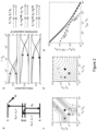
- Fig. 2 shows a simplified energy-level model and rate-equation calculations for a two-step absorption photoinitiator.
- Fig. 2a shows energy levels, with ground state A, intermediate states B and B', and upper state C.
- R ⁇ Radicals
- k 1 ⁇ ⁇ 1 I and k 2 ⁇ ⁇ 2 I are proportional to the respective state's extinction coefficient and the laser intensity I .
- FIG. 2b shows a temporal evolution of the states' population (left axis) and the nonlinearity exponent N (right axis) for three exemplary chosen parameter sets, as defined in the legends.
- For t ⁇ k D > 10, we have D ⁇ tI 2 (hence, N 2).
- Fig. 2c shows a logarithmic plot of the exponent N versus k 1 / k D and k 2 / k D .
- FIG. 2d shows a normalized exposure time t exp k D versus k 1 / k D and k 2 / k D .
- the markers refer to the three conditions defined in Fig. 2b.
- k D is the intermediate-state B decay rate coefficient - the inverse of the intermediate state lifetime ⁇ .
- This differential equation system is solved analytically using Mathematica to obtain explicit expressions for the functions [A](t), [B](t), and [C](t) (see Figs. 2b and 2c ).
- the results shown in Figs. 2d and 2e have been computed by numerical searches of zero crossings using Matlab.
- Fig. 3 shows benzil as two-step absorption photoinitiator.
- Fig. 3a shows a benzil photoinitiator molecule used here.
- Fig. 3b shows the corresponding Jablonski diagram.
- the real intermediate state in Fig. 1b is replaced by the excited state singlet manifold, S 1 , and the ground state triplet manifold, T 1 .
- ISC intersystem crossing
- a polymerization inhibitor (BTPOS) suppresses unwanted reactions starting from the occupation of the T 1 state.
- the second step in two-step absorption brings an electron from the T 1 state to an excited triplet manifold T n from where radicals (R ⁇ ) are generated, starting the polymerization reaction.
- Fig. 3c shows measured ground state extinction and flash photolysis triplet excitation spectra of benzil in benzene.
- Fig. 3b For benzil shown in Fig. 3a , the two-step absorption photoinitiator molecule used here, a Jablonski diagram is depicted in Fig. 3b .
- the real intermediate energy level in Fig. 1b is replaced by two nearby real intermediate levels, the singlet S 1 and the triplet T 1 state. Intersystem crossing brings electrons from the S 1 to the T 1 state within a few nanoseconds. The quantum efficiency of this nonradiative process is 92%.
- Fig. 3c shows the ground state molar decadic extinction and the excited-state extinction spectra of benzil in solution.
- the wavelength of 405 nm lies in the tail of both spectral maxima and therefore allows for mediating both types of transitions.
- the ground state extinction is about 100 times lower than the triplet-state extinction. This has two attractive consequences.
- the photoresist is sufficiently transparent over distances of about 300 ⁇ m, i.e., over typical free working distances of microscope objective lenses. This allows for dip-in 3D laser nanoprinting.
- radicals are generated by fragmentation of molecules into radicals by cleaving chemical bonds, with typical bond energies being above 3 eV (69 kcal/mol).
- the triplet ground state energy of benzil E T1 2.3 eV (54 kcal/mol), is well below that energy.
- the triplet energy must be higher than the bond energy.
- benzil has been referred to as "reluctant" Norrish type I initiator - which has been our motivation for investigating benzil as a candidate for two-step absorption in the first place.
- benzil, as well as other alpha-diketones readily abstracts hydrogen atoms from its triplet ground state. This leads to an undesired one-photon triggered polymerization reaction.
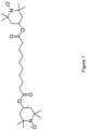
- the photoresist compositions used here and abbreviated as PR1 to PR4 in what follows contain bis(2,2,6,6-tetramethyl-4-piperidyl-1-oxyl) sebacate (BTPOS) (see Fig. 7 ) as a polymerization inhibitor.
- BTPOS bis(2,2,6,6-tetramethyl-4-piperidyl-1-oxyl) sebacate
- TEMPO 2,2,6,6-tetramethyl-4-piperidyl-1-oxyl
- TEMPO can suppress the undesired hydrogen abstraction initiated from an electron in the benzil triplet T 1 state, which may otherwise occur and lead to unwanted radicals initiating the polymerization reaction (see Fig. 8 ). This initiation would be based on a one-photon process.
- TEMPO favorably lowers the lifetime of the intermediate T 1 state. Therefore, the concentration of TEMPO (or BTPOS) is a design parameter in the photoresist composition.
- the photoresists PR1, PR2 and PR4 contain pentaerythritol triacrylate (PETA) as the monomer.
- PETA pentaerythritol triacrylate
- PETA trimethylolpropane triacrylate
- TMPTA trimethylolpropane triacrylate
- Benzil (98%) was purchased from Aldrich. Bis(2,2,6,6-tetramethyl-4-piperidyl-1-oxyl) sebacate (BTPOS, 98%) was purchased from TCI chemicals. A ground state extinction spectrum is given in Fig. 12 .
- Pentaerythritol triacrylate (PETA) was purchased from Sigma-Aldrich.
- IP-DIP NPI was purchased from Nanoscribe GmbH & Co. KG.
- Trimethylolpropane triacrylate (TMPTA, 93%) was purchased from Alfa Aesar.
- Irgacure 369 was purchased from Ciba Specialty Chemicals.
- Fig. 4 shows the effective nonlinearity of a photoresist composition according to an embodiment of the present invention.
- Fig. 4 shows the measured threshold laser power versus exposure time (dots) on a double-logarithmic scale for the photoresist composition PR1.
- the error bars mark the minimum and maximum values of at least three independent measurements.
- Fig. 5 shows a two-step absorption printing resolution in two and three dimensions.
- Fig. 5c shows grayscale optical reflection-mode micrographs (objective lens numerical aperture NA 0.4) of a set of 3D woodpile structures. The used laser power is increased in steps of 5% in the horizontal direction.
- the smallest rod spacing for 3D woodpiles made by using two-photon absorption and near infrared femtosecond lasers is equal to 375 nm (without invoking stimulated-emission depletion).
- Fig. 6 shows a gallery of oblique-view electron micrographs of 3D-printed nanostructures.
- Fig. 6a shows helices with a radius of 800 nm and a pitch of 800 nm.
- Fig. 6b shows three buckyball models with diameters of 15 ⁇ m, 10 ⁇ m, and 5 ⁇ m.
- Fig. 6c shows five stacked chiral metamaterial unit cells with a lattice constant of 16 ⁇ m.
- Fig. 6d shows a 3D model of the KIT-Logo.
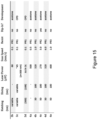
- Fig. 6e shows a miniaturized model of the #3DBenchy structure. Detailed 3D-printing parameters for all structures are provided in Fig. 15 .
- Fig. 6 we present a gallery of electron micrographs of other 3D-printed architectures. Some of these microstructures are intentionally taller than the nanostructures shown in Fig. 5 . Thereby, Fig. 6 shows that combining two-step absorption with the widespread immersion or dip-in mode of 3D laser nanoprinting is readily possible. Clearly, dip-in 3D-printing requires that the refractive index of the two-step absorption photoresist PR2 is matched to that underlying the design of the microscope objective lens. We note, however, that fast 3D-printing of structures with a high filling fraction, as in Fig. 6e , is challenging for the photoresist PR2 and even for the photoresist PR1. We attribute this to a higher concentration of abstractable hydrogen atoms within the used monomer. In Fig. 6 , the printing laser-focus velocities are around 0.5 to 4 mm/s (or 2 400 to 19 400 voxels/s).
- two-step absorption in benzil replacing two-photon absorption may be considered as the fundamental photoinitiation mechanism in 3D laser nanoprinting.
- the presented 2D and 3D benchmark nanostructures match or even surpass previous results obtained with two-photon absorption in terms of achievable spatial resolution.
- our two-step absorption results were obtained with a continuous-wave semiconductor laser diode that is many orders of magnitude less expensive and smaller in volume than the femtosecond lasers commonly used today for obtaining efficient two-photon absorption.
- the present inventors consider two-step absorption replacing two-photon absorption in 3D laser nanoprinting as a breakthrough.
- Second, dramatic miniaturization of 3D laser nanoprinters is straightforward given that the diode laser used here has a volume of only some cubic millimeters. Combined, the drastic cost and size reduction will likely dramatically amplify the spread of 3D laser nanoprinters in the industrial field in the upcoming years.
- Fig. 7 shows a chemical structure of bis(2,2,6,6-tetramethyl-4-piperidyl-1-oxyl) sebacate (BTPOS).
- Fig. 8 shows scanning electron micrographs of 3D-printed line gratings with different grating periods when omitting the quencher BTPOS in the photoresist composition PR1 containing benzil.
- the fast scanning direction is along the - x direction
- the slow scanning direction is along the + y direction.
- the used laser powers are about 2 ⁇ W.
- All other 3D-printing parameters are identical to the line gratings shown in Fig. 5 .
- Fig. 9 shows laser power versus exposure time for the photoresist PR4, containing Irgacure 369 (50 mM) instead of benzil.
- the straight lines are guides to the eye.
- t exp > 4 ms the data are consistent with a slope of -1/2.
- t exp ⁇ 100 ⁇ s the data indicate a slope close to -1.
- Fig. 10 shows a top-view scanning electron micrograph of attempts to 3D-print woodpile structures using the photoresist PR4, containing Irgacure 369 as the photoinitiator.
- Fig. 10a shows an overview image. The structures have been printed from top left to bottom right.
- Fig. 10b shows a zoom-in of Fig. 10a .
- the threshold dose increases in the proximity of previously 3D-printed structures.
- Fig. 12 shows a ground state extinction spectrum of BTPOS in acetonitrile. The arrow indicates the excitation wavelength.
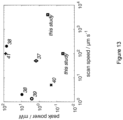
- Fig. 13 shows an overview on a double-logarithmic scale of 3D laser polymer printing using (quasi-)continuous-wave lasers. It can be seen that two-step absorption (labelled as "this study") enables scan speeds that are up to three orders of magnitude faster than in previous studies (numbers 37 to 41), and (peak) laser powers that are up to three orders of magnitude lower. Note that this overview does not include the achieved spatial resolution.
- Fig. 14 a very simplified schematic picture of a system 10 is shown.
- the system 10 comprises a photoresist composition 12, a continuous-wave light source 14, a focusing unit 16, and a positioning unit 18 comprising a movable stage 18a and a tiltable mirror 18b.
- the continuous-wave light source 14 may be a laser diode.
- the dashed arrow line represents the optical path of the light emitted by the continuous-wave light source 14.
- the laser diode (L405P150, Thorlabs GmbH) is mounted on a temperature-controlled mount (LDM56/M, Thorlabs GmbH).
- LDM56/M temperature-controlled mount
- a spectrum of the laser emission is displayed in Fig. 11 .
- the diode's temperature is controlled by a TEC controller (TED200C, Thorlabs GmbH) and the electrical current is controlled using a laser diode driver (LDC 200, Profile GmbH).
- An aspheric 8 mm focal length collimator lens (A240TM-A, Thorlabs GmbH) collimates the laser diode output.
- the laser diode's beam is focused using a 40 mm focal length plano-convex (LA1422-A, Thorlabs GmbH) lens through a 10 ⁇ m diameter pinhole (P10C Thorlabs GmbH) and collimated by a 75 mm focal length achromatic lens (AC254-075-A, Thorlabs GmbH).
- the beam is deflected by a pair of galvanometric mirrors (Saturn 5B 56S, Pangolin Laser Systems Inc.) which are imaged by two achromatic lenses (ACL254-100-A and ACL254-150-A, Thorlabs GmbH) through a quarter-wave plate (WPQSM05-405, Thorlabs GmbH) on a microscope objective lens' (HCX PL APO 100 ⁇ /1.4-0.7 Oil CS, Leica Microsystems GmbH) entrance pupil. For 3D-printing the woodpile structures, no quarter-wave plate was used.
- the objective lens focusses the beam into the sample photoresist (25 ⁇ l), which, for non-dip-in experiments, is contained in a PDMS-ring (5 mm diameter) placed on a methacrylate silanized glass coverslip (No. 1.5H, Paul Marienfeld GmbH & Co. KG).
- the coverslip is mounted on a 3D piezoelectric stage (P-527.3CL, Physik Instrumente GmbH & Co. KG).
- the piezoelectric stage was replaced by one with a larger travel range (P-563.3CD, Physik Instrumente GmbH & Co. KG).
- Galvanometric xy-scanning was used for all 3D structures shown in Fig. 6 . All other structures were 3D-printed by scanning the sample with the piezoelectrically actuated stages.
- the sample is illuminated using an LED with a peak wavelength ⁇ ⁇ 640 nm and observed in-situ in transmission-mode on a CCD camera.
- the laser power was adjusted using a half-wave plate (WPHSM05-405, Thorlabs GmbH) and a polarizing beamsplitter cube (PBS251, Thorlabs GmbH), both located in front of the galvanometric mirror pair.
- WPHSM05-405, Thorlabs GmbH a half-wave plate
- PBS251, Thorlabs GmbH a polarizing beamsplitter cube
- absorptive neutral density glass filters FSQ-OD20 to FSQ-OD300, Coherent Inc.
- the laser focus was checked routinely to ensure that the filter glass does not cause any wavefront aberrations.
- the woodpile photonic crystals were developed in acetone (UV/IR grade) with subsequent supercritical drying in CO 2 using the EM CPD300 (Leica Microsystems GmbH).
- Fig. 15 shows a list of 3D-printing parameters for all structures shown in Figs. 1 to 6 .
- CPD Critical Point Drying
- the present inventors have recognized that involving at least two sequential single-photon excitations or two-step photon absorption replacing two-photon absorption as the primary optical excitation process may overcome the above-mentioned issues and drawbacks of state-of-the-art 3D-printing.
- Two-step absorption may enable the same quadratic optical nonlinearity as two-photon absorption.
- the present invention allows for printing state-of-the-art 3D nanostructures and beyond with high resolution and opens the door to drastic miniaturization and cost cutting of 3D-printing.
Landscapes
- Physics & Mathematics (AREA)
- Chemical & Material Sciences (AREA)
- Engineering & Computer Science (AREA)
- Materials Engineering (AREA)
- Manufacturing & Machinery (AREA)
- Optics & Photonics (AREA)
- General Physics & Mathematics (AREA)
- Spectroscopy & Molecular Physics (AREA)
- Mechanical Engineering (AREA)
- Inorganic Chemistry (AREA)
- Health & Medical Sciences (AREA)
- Toxicology (AREA)
- Plasma & Fusion (AREA)
- Exposure And Positioning Against Photoresist Photosensitive Materials (AREA)
Priority Applications (3)
| Application Number | Priority Date | Filing Date | Title |
|---|---|---|---|
| EP21205242.7A EP4173824A1 (fr) | 2021-10-28 | 2021-10-28 | Composition de photorésine, système comprenant une composition de photorésine, procédé de fabrication d'une structure tridimensionnelle, et utilisation d'une composition de photorésine dans l'impression 3d |
| PCT/EP2022/079954 WO2023073034A1 (fr) | 2021-10-28 | 2022-10-26 | Composition de résine photosensible, système comprenant une composition de résine photosensible, procédé de production d'une structure tridimensionnelle et utilisation d'une composition de résine photosensible dans l'impression 3d |
| US18/703,452 US20240408815A1 (en) | 2021-10-28 | 2022-10-26 | Photoresist composition, system comprising a photoresist composition, method for producing a three-dimensional structure, and use of a photoresist composition in 3d-printing |
Applications Claiming Priority (1)
| Application Number | Priority Date | Filing Date | Title |
|---|---|---|---|
| EP21205242.7A EP4173824A1 (fr) | 2021-10-28 | 2021-10-28 | Composition de photorésine, système comprenant une composition de photorésine, procédé de fabrication d'une structure tridimensionnelle, et utilisation d'une composition de photorésine dans l'impression 3d |
Publications (1)
| Publication Number | Publication Date |
|---|---|
| EP4173824A1 true EP4173824A1 (fr) | 2023-05-03 |
Family
ID=78414341
Family Applications (1)
| Application Number | Title | Priority Date | Filing Date |
|---|---|---|---|
| EP21205242.7A Pending EP4173824A1 (fr) | 2021-10-28 | 2021-10-28 | Composition de photorésine, système comprenant une composition de photorésine, procédé de fabrication d'une structure tridimensionnelle, et utilisation d'une composition de photorésine dans l'impression 3d |
Country Status (3)
| Country | Link |
|---|---|
| US (1) | US20240408815A1 (fr) |
| EP (1) | EP4173824A1 (fr) |
| WO (1) | WO2023073034A1 (fr) |
Families Citing this family (1)
| Publication number | Priority date | Publication date | Assignee | Title |
|---|---|---|---|---|
| WO2022212557A1 (fr) | 2021-03-31 | 2022-10-06 | Quadratic 3D, Inc. | Compositions photodurcissables, procédés et stabilisant |
Citations (6)
| Publication number | Priority date | Publication date | Assignee | Title |
|---|---|---|---|---|
| US20150030985A1 (en) * | 2012-02-28 | 2015-01-29 | Robert J. DeVoe | Multiphoton Curing Methods Using Negative Contrast Compositions |
| US20170168392A1 (en) * | 2015-12-14 | 2017-06-15 | University Of Maryland, College Park | Multicolor Photolithography Materials and Methods |
| US20180015661A1 (en) * | 2016-07-15 | 2018-01-18 | Purdue Research Foundation | Continuous and scalable 3d nanoprinting |
| CN111116833A (zh) * | 2019-12-30 | 2020-05-08 | 先临三维科技股份有限公司 | 一种3d打印用树脂组合物、抗氧阻聚树脂、3d打印制品及制备方法 |
| WO2020126154A1 (fr) * | 2018-12-17 | 2020-06-25 | Karlsruher Institut für Technologie | Lithographie 3d parallélisée par polymérisation induite par la lumière multicolore et multifaisceaux |
| EP3766669A1 (fr) * | 2019-07-18 | 2021-01-20 | Bostik Sa | Procédés et systèmes d'impression 3d |
Family Cites Families (1)
| Publication number | Priority date | Publication date | Assignee | Title |
|---|---|---|---|---|
| US12545766B2 (en) * | 2019-04-04 | 2026-02-10 | Lawrence Livermore National Security, Llc | Curable polymer resins for 3D-printable hierarchical nanoporous foams and aerogels |
-
2021
- 2021-10-28 EP EP21205242.7A patent/EP4173824A1/fr active Pending
-
2022
- 2022-10-26 WO PCT/EP2022/079954 patent/WO2023073034A1/fr not_active Ceased
- 2022-10-26 US US18/703,452 patent/US20240408815A1/en active Pending
Patent Citations (6)
| Publication number | Priority date | Publication date | Assignee | Title |
|---|---|---|---|---|
| US20150030985A1 (en) * | 2012-02-28 | 2015-01-29 | Robert J. DeVoe | Multiphoton Curing Methods Using Negative Contrast Compositions |
| US20170168392A1 (en) * | 2015-12-14 | 2017-06-15 | University Of Maryland, College Park | Multicolor Photolithography Materials and Methods |
| US20180015661A1 (en) * | 2016-07-15 | 2018-01-18 | Purdue Research Foundation | Continuous and scalable 3d nanoprinting |
| WO2020126154A1 (fr) * | 2018-12-17 | 2020-06-25 | Karlsruher Institut für Technologie | Lithographie 3d parallélisée par polymérisation induite par la lumière multicolore et multifaisceaux |
| EP3766669A1 (fr) * | 2019-07-18 | 2021-01-20 | Bostik Sa | Procédés et systèmes d'impression 3d |
| CN111116833A (zh) * | 2019-12-30 | 2020-05-08 | 先临三维科技股份有限公司 | 一种3d打印用树脂组合物、抗氧阻聚树脂、3d打印制品及制备方法 |
Also Published As
| Publication number | Publication date |
|---|---|
| WO2023073034A1 (fr) | 2023-05-04 |
| US20240408815A1 (en) | 2024-12-12 |
Similar Documents
| Publication | Publication Date | Title |
|---|---|---|
| Hahn et al. | Light-sheet 3D microprinting via two-colour two-step absorption | |
| Hahn et al. | Two-step absorption instead of two-photon absorption in 3D nanoprinting | |
| Müller et al. | STED-inspired laser lithography based on photoswitchable spirothiopyran moieties | |
| Gan et al. | Three-dimensional deep sub-diffraction optical beam lithography with 9 nm feature size | |
| JP2021502466A (ja) | 光重合性組成物、該組成物を重合して得られる材料、および該組成物を用いた3d印刷方法 | |
| US6387593B1 (en) | Self-trapping and self-focusing of optical beams in photopolymers | |
| US11999098B2 (en) | Parallelized 3D lithography using multi-beam, multi-color light-induced polymerization | |
| Hahn et al. | Challenges and opportunities in 3D laser printing based on (1+ 1)-photon absorption | |
| Spangenberg et al. | Recent advances in two-photon stereolithography | |
| Mutoh et al. | Rapid fluorescence switching by using a fast photochromic [2.2] paracyclophane-bridged imidazole dimer | |
| Guan et al. | Light and matter co-confined multi-photon lithography | |
| Forman et al. | Radical diffusion limits to photoinhibited superresolution lithography | |
| Chi et al. | Tailored thioxanthone‐based photoinitiators for two‐photon‐controllable polymerization and nanolithographic printing | |
| He et al. | 3D sub‐diffraction printing by multicolor photoinhibition lithography: from optics to chemistry | |
| König et al. | Optically induced nanostructures: biomedical and technical applications | |
| US20240408815A1 (en) | Photoresist composition, system comprising a photoresist composition, method for producing a three-dimensional structure, and use of a photoresist composition in 3d-printing | |
| CN116430687B (zh) | 一种基于双光束的高通量超分辨三维刻写方法与系统 | |
| Somers et al. | Photo-activated polymerization inhibition process in photoinitiator systems for high-throughput 3D nanoprinting | |
| Islam et al. | STED-inspired cationic photoinhibition lithography | |
| Durko-Maciag et al. | Two is better than one: ESIPT dyes as photoinitiators in two-photon polymerization | |
| De Miguel et al. | Linewidth and writing resolution | |
| US7964333B1 (en) | FRET-based two photon three dimensional optical data storage | |
| CN118984770A (zh) | 用于高分辨率的快速逐层3d打印的方法和设备 | |
| Takada et al. | The study on spatial resolution in two-photon induced polymerization | |
| Varapnickas et al. | 3d microoptics via ultrafast laser writing: Miniaturization, integration, and multifunctionalities |
Legal Events
| Date | Code | Title | Description |
|---|---|---|---|
| PUAI | Public reference made under article 153(3) epc to a published international application that has entered the european phase |
Free format text: ORIGINAL CODE: 0009012 |
|
| STAA | Information on the status of an ep patent application or granted ep patent |
Free format text: STATUS: THE APPLICATION HAS BEEN PUBLISHED |
|
| AK | Designated contracting states |
Kind code of ref document: A1 Designated state(s): AL AT BE BG CH CY CZ DE DK EE ES FI FR GB GR HR HU IE IS IT LI LT LU LV MC MK MT NL NO PL PT RO RS SE SI SK SM TR |
|
| STAA | Information on the status of an ep patent application or granted ep patent |
Free format text: STATUS: REQUEST FOR EXAMINATION WAS MADE |
|
| 17P | Request for examination filed |
Effective date: 20230907 |
|
| RBV | Designated contracting states (corrected) |
Designated state(s): AL AT BE BG CH CY CZ DE DK EE ES FI FR GB GR HR HU IE IS IT LI LT LU LV MC MK MT NL NO PL PT RO RS SE SI SK SM TR |
|
| STAA | Information on the status of an ep patent application or granted ep patent |
Free format text: STATUS: EXAMINATION IS IN PROGRESS |
|
| 17Q | First examination report despatched |
Effective date: 20250827 |