EP4174579B1 - System und verfahren zum dauerhaften markieren von flexoplatten mit isolierten mikrostrukturen und damit markierte platten - Google Patents
System und verfahren zum dauerhaften markieren von flexoplatten mit isolierten mikrostrukturen und damit markierte platten Download PDFInfo
- Publication number
- EP4174579B1 EP4174579B1 EP22172781.1A EP22172781A EP4174579B1 EP 4174579 B1 EP4174579 B1 EP 4174579B1 EP 22172781 A EP22172781 A EP 22172781A EP 4174579 B1 EP4174579 B1 EP 4174579B1
- Authority
- EP
- European Patent Office
- Prior art keywords
- printing
- plate
- supercell
- mask
- floor
- Prior art date
- Legal status (The legal status is an assumption and is not a legal conclusion. Google has not performed a legal analysis and makes no representation as to the accuracy of the status listed.)
- Active
Links
Images









Classifications
-
- G—PHYSICS
- G03—PHOTOGRAPHY; CINEMATOGRAPHY; ANALOGOUS TECHNIQUES USING WAVES OTHER THAN OPTICAL WAVES; ELECTROGRAPHY; HOLOGRAPHY
- G03F—PHOTOMECHANICAL PRODUCTION OF TEXTURED OR PATTERNED SURFACES, e.g. FOR PRINTING, FOR PROCESSING OF SEMICONDUCTOR DEVICES; MATERIALS THEREFOR; ORIGINALS THEREFOR; APPARATUS SPECIALLY ADAPTED THEREFOR
- G03F9/00—Registration or positioning of originals, masks, frames, photographic sheets or textured or patterned surfaces, e.g. automatically
- G03F9/70—Registration or positioning of originals, masks, frames, photographic sheets or textured or patterned surfaces, e.g. automatically for microlithography
- G03F9/7003—Alignment type or strategy, e.g. leveling, global alignment
- G03F9/7038—Alignment for proximity or contact printer
-
- G—PHYSICS
- G03—PHOTOGRAPHY; CINEMATOGRAPHY; ANALOGOUS TECHNIQUES USING WAVES OTHER THAN OPTICAL WAVES; ELECTROGRAPHY; HOLOGRAPHY
- G03F—PHOTOMECHANICAL PRODUCTION OF TEXTURED OR PATTERNED SURFACES, e.g. FOR PRINTING, FOR PROCESSING OF SEMICONDUCTOR DEVICES; MATERIALS THEREFOR; ORIGINALS THEREFOR; APPARATUS SPECIALLY ADAPTED THEREFOR
- G03F9/00—Registration or positioning of originals, masks, frames, photographic sheets or textured or patterned surfaces, e.g. automatically
- G03F9/70—Registration or positioning of originals, masks, frames, photographic sheets or textured or patterned surfaces, e.g. automatically for microlithography
- G03F9/7073—Alignment marks and their environment
- G03F9/7076—Mark details, e.g. phase grating mark, temporary mark
-
- G—PHYSICS
- G03—PHOTOGRAPHY; CINEMATOGRAPHY; ANALOGOUS TECHNIQUES USING WAVES OTHER THAN OPTICAL WAVES; ELECTROGRAPHY; HOLOGRAPHY
- G03F—PHOTOMECHANICAL PRODUCTION OF TEXTURED OR PATTERNED SURFACES, e.g. FOR PRINTING, FOR PROCESSING OF SEMICONDUCTOR DEVICES; MATERIALS THEREFOR; ORIGINALS THEREFOR; APPARATUS SPECIALLY ADAPTED THEREFOR
- G03F9/00—Registration or positioning of originals, masks, frames, photographic sheets or textured or patterned surfaces, e.g. automatically
- G03F9/70—Registration or positioning of originals, masks, frames, photographic sheets or textured or patterned surfaces, e.g. automatically for microlithography
- G03F9/7088—Alignment mark detection, e.g. TTR, TTL, off-axis detection, array detector, video detection
Definitions
- Applicant has devised a number of systems and methods for providing persistent marking of flexo plates detailed in previously applications, including but not limited to:
- flexographic printing flexible photopolymer printing plates are mounted on metal cylinders that press the printing plate against a second cylinder which holds the print substrate.
- printing presses have several plate cylinders for the different ink colours, which cylinders all must be aligned with respect to another, typically by mounting the plates aligned to a reference mark on the cylinder.
- EP2397327A2 discloses non-printing registration marks applied by means of laser scribing or cutting with a knife on a cutting table into the plate floor or the plate's rear side. This is cumbersome because plates and marks had to be aligned with respect to another. Accordingly, there is a need in the art for other methods of forming alignment marks.
- alignment marks have historically taken the shape of "crosshairs,” which can be added to the image file. These crosshairs print in the same way as image details, but are located outside the image areas. The use of alignment marks outside of the image area consumes more plate material than is needed just for the image area, thus creating inefficiency or waste.
- Non-printing indicia defined by areas of presence and absence of polymer in the plate floor are created using microdots imaged during a LAMS layer imaging step.
- the non-printing indicia are readable downstream of the washing or other non-cured-polymer-removal step but not to print in the printing step.
- the non-printing indicia may define a repeating pattern of alphanumeric characters, non-text graphics, or a combination thereof.
- a difference in growth of plate structures corresponding to different types of microdots may be used for characterizing processing conditions.
- indicia as used herein is intended to have its broadest meaning of "an indication” or “distinguishing mark,” without limitation to how that indication or mark is capable of being read, and thus the “equivalents” of the indicia as expressly described are intended to be broadly construed. While certain machine-readable indicia or codes may take advantage of formats that are exclusively machine readable to permit a large volume of information to be stored in a small amount of space, it should be understood that the term “machine readable,” as used herein to refer to indicia and codes, is not limited to indicia having a format that is exclusively machine-readable.
- the code for a printed code such as a bar code or a QR code or printed indicia comprising text and/or graphics readable by a human or machine, may be added during ripping the image file and is thus included in the content of the image information, such as in the .LEN file or encrypted LENx file associated with an Esko PlatePrep workflow.
- Adding a code to an image file may be accomplished using, for example, Esko DeskPack TM barX software, which software comprises machine-readable instructions embodied in storage media, such as a hard drive, a flash drive, or any type of media, as is well known in the art.
- the imaged information may be provided in the form of non-printing structures on the plate floor formed using microdots, including in the form of a non-printing watermark derived from the use of non-printing microdots in a printing portion of the plate.
- Such structures formed from microdots may be created on a flexo plate using an Esko ® XPS exposure system.
- microdots primarily refers to small mask openings in the LAMs layer of a flexo plate, wherein each opening is not wide enough to grow a printable screen dot in isolation (under normal power), but clusters of them (or single pixels with sufficient boost) are operable to raise the plate floor level.
- microdot may also refer to any dot used in any imaging step by any process capable of creating a non-printing dot structure on a plate, including but not limited to direct curing processes and non-LAMS mask-based processes.
- the term “microdot” may be used to refer to a feature in the image information used by the imager for creating the plate or mask structure, as well as the plate structures formed thereby.
- a cluster of microdots may be used to form sections of elevated floor relative to other sections of the floor that remain non-elevated and arranged in a formation resembling the dark and light sections in a QR-code or a barcode.
- the arrangement of microdots is object-based, meaning the amount, distance and pixel cluster size of the microdots varies with size and shape of an alphanumeric sign or code object such as a barcode or a crosshair.
- microdots may be used to form the floor and an absence of such microdots may be used to provide depressions in the floor.
- microdots may also be used to create a combination of elevated and depressed structures relative to a predetermined floor level. The microdots in the mask result in microstructures (elevations or depressions) in the exposed plate.
- watermark is used herein as an analog to the original definition of the term for the identifying images or patterns on paper that appear as various shades of lightness/darkness when viewed by transmitted or reflected light (at certain angles or atop a dark background), caused by thickness or density variations in the paper. Such watermarks are often visible in the paper constituting an original document, but not in reproductions (e.g. photocopies) made from that paper.
- the non-printing watermark formed in accordance with embodiments of the invention may be more visible under certain conditions (e.g. reflected light at a certain angle) and comprise a variation in thickness of the plate, with the markings not reproduced in printed matter made by the subject plate.
- microdots are clusters of tiny mask openings in the LAMs layer of the photopolymer plate, the amount of UV light (or other actinic radiation) is not great enough for curing structures on the plate floor that reach the top of the plate, but it is sufficient to create structures on the plate floor that are typically visible.
- One application for non-printing structures on the floor may be for checking the alignment of a plate on the printing cylinder.
- a line may be formed on the floor in an orientation parallel to the circumference of the printing cylinder. During mounting the plate, or later in the press, this line can be used to check the correct parallel alignment of the plate with respect to the printing cylinder or sleeve.
- microdots are created by openings in the mask by ablating clusters of pixels in regular distance in the LAMs layer, or by ablating only single pixels in the LAMs and boosting the laser power for ablation such that the total width of the mask opening is adjusted to the desired value, such as for example, by using a Gaussian Beam profile for the ablation.
- Various method may be used for providing the image information for the non-printing structures in the image file used for controlling ablation of the mask.
- Image information is often provided by PDF files.
- PDF files often contain different layers (e.g. for different ink colors). Accordingly, the non-printing image may be contained in a dedicated layer of the PDF file. This image is then ripped by the RIP with the screen of microdots.
- Indicia may be created in the plate floor as an inverse structure, in form of a depression at a predetermined height below the floor, rather than a predetermined elevation above the floor.
- One exposure process for making such depressions is to create a first subfloor at a relatively lower height than the desired final floor by using less exposure energy than is required to create the height of the desired final floor.
- areas of the desired final floor are formed via an exposure step using microdot openings in the mask. In locations in which the desired inverse indicia is located, no mask openings (microdot or printing) are formed in the corresponding portions of the mask.
- a constant screen of microdots is combined disjunctively with the printing image information to create the normal floor (e.g., pixels already turned “on” based upon image information remain “on,” and pixels corresponding to microdots are turned “on” only in locations previously “off”).
- the microdot screen is omitted (and the corresponding pixels remain "off”).
- microdots may additionally be arranged in concentric circles around certain printing screen dots (e.g.
- the micro screen for creating the floor may be adjusted according to the halftone screening percentage instead of calculating microdots for every single printing highlight dot.
- any process known in the art for creating a printing plate may be used for creating non-printing indicia as described herein, including but not limited to exposure of photopolymer plates by actinic radiation in any range of wavelengths, including plates created by direct imaging or using masks imaged by any process known in the art.
- the masking component may be a film or LCD matrix having transparent and non-transparent areas.
- the masking component may be the same size (e.g. width and length) as the polymer plate (or the combination of source, masking component, and optics (optional) may project an image that is the same size as the polymer plate, or any desired size).
- the masking component may only cover (or only create a projection that covers) less than the full area of the plate, and the overall system may be positionable to create non-printing indicia in specific desired locations, which locations may be coordinated, such as via a controller which may have information about printing and non-printing information, to correspond to locations on the plate lacking printing features.
- the masking component may have a multitude of markings (e.g. brand logos), such that the markings may be distributed throughout the polymer plate floor like a watermark.
- the method may be implemented in a single exposure step without a need to move the plate relative to the UV source and/or masking component.
- the source emits radiation that passes through transparent (or relatively more translucent) areas or holes in the masking component and is blocked by opaque, non-transparent (or relatively less translucent) areas, and is optionally focused by optics (in some embodiments), such that the radiation forms non-printing features in the photopolymer above the floor of plate.
- the plate may have a backing layer, as is known in the art. Printing features may be formed by any method known in the art, typically by exposure to actinic radiation through holes in the mask.
- the non-printing image information may be advantageously imposed only at locations on the plate where no printing details are present, to avoid changes in size of highlight screen printing dots.
- the source may comprise an LED matrix of individual LEDs in an array that covers the full width and length dimensions of the plate.
- the source may comprise an LED matrix of individual LEDs in an array that covers the full width and length dimensions of the plate.
- relative motion between the plate and the back side source may not be required for exposure of the back surface of the plate.
- systems in which the front source also comprising an LED matrix of individual LEDs in an array that covers the full width and length dimensions of the plate may be provided, in which case relative motion is not required for either front side or back side exposure.
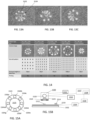
- Fig.1 shows a cross section of a photopolymer plate 1900 comprising the plate floor 1901, which holds elevated non-printing structures 1902 and printing structures 1903.
- LAMs Laser Ablateable Mask
- a substrate 1905 or foil of e.g. polyester, such as polyethylene terephthalate (PET)
- PET polyethylene terephthalate
- FIG. 1 Three different elevation levels are shown in FIG. 1 : floor level 1910, non-printing level 1920, and print surface level 1930.
- the non-printing structures can also be applied as sunken structures, as depicted in FIG. 2 .
- the non-printing structures do not extend above the floor level, which has the advantage that the risk of accidental printing is minimized.
- the floor 2001 is created partially or completely through mask openings 2011 in the LAMs layer 2004.
- the elevation 2020 of non-printing structures 2002 stays is defined below the floor level. This level 2020 is either determined by back side exposure and a non-perforated LAMs above or by front exposure through mask openings 2022, which are smaller than mask openings 2011.
- Printing structures 2003 at printing level 2030 are defined by one or more openings 2013 that are larger than openings 2011 or 2022. Openings may include, but are not limited to, openings that conform to a base pattern, such as is described in U.S. Published Patent Application No. 20190315141A1 .
- This method for creating alignment marks in flexographic printing plates may be used for packaging printing as well as for flexographic printing plates used for corrugated printing.
- the same principle can also be applied to photopolymer letterpress plates e.g. used for label printing.
- it can be applied to sleeves and plates made from liquid photopolymer.
- the high frequency mask openings as described herein may also be used solely to create the floor, advantageously eliminating a need for back exposure and a back exposure "teach-in" for plates from different batches.
- back exposure through a plate's rear side often requires a "teach-in” (re-checking rear exposure parameters) each time a new batch of plates is used, because UV transmissivity of the rear substrate may vary from one plate batch to another.
- the polymer and the LAMs layer have more stable properties that do not significantly vary from one batch to another.
- exposing the floor through the front side with constant parameters is more predictable than methods that use back exposure, as using all front exposure eliminates the need for checking the floor curing parameters when a new batch of plates starts.
- this process may also lead to faster main UV exposure when combined (or not) with a back-exposure, because often back exposure from the plate rear side slows down the overall process time for the UV exposure process.
- UV LEDs have a lower total available UV Power for back exposure over time compared to a bank exposure device, but the energy can be controlled more precisely.
- the UV blocker in the PE back sheet has become a disadvantage that slows down the overall process. Therefore, exposing and creating the floor through the front side using non-printing structures, where no UV blocker is present, can speed up the overall UV curing cycle and may also eliminate the need for a rear side exposure head.
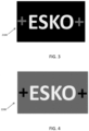
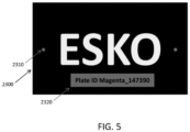
- FIGS. 3 to 5 show different application examples of non-printing alignment marks.
- the figures show respective plan views of a plate 2100, 2200, 2300 after imaging, before processing.
- Black areas represent the unablated LAMs disposed on top of the photopolymer, which after exposure and further processing, resolves to portions of the printing plate at the floor level.
- White areas represent areas with the LAMs ablated with printing structure sized openings, which resolve to structures of cured polymer at the printing surface of the plate.
- Gray areas represent areas of the LAMs perforated by many small mask openings, which resolve to cured polymer at a height below the printing surface but above the floor level surface defined by the black areas.
- Plates 2100 and 2200 illustrate exemplary plates suitable for use in a corrugated application
- plate 2300 illustrates an exemplary plate suitable for use in a flexible packaging application.
- Plate 2300 includes not only alignment marks 2310, but also non-printing identification indicia 2320.
- the method as described above is not limited to creating alignment marks, but can also be used to create other non-printing structures, such as but not limited to, user-specific information like barcodes, logos, letters or identification numbers, and the like.
- Various parameters have an effect on the visibility and size of the non-printing objects on the plate floor, including but not limited to: plate thickness, plate (polymer) type, targeted relief thickness (the distance between plate floor level 1900 and printing surface level 1930), size of the mask opening (number of connected pixels that build one common area of mask opening), distance between the mask openings, UV exposure parameters (UV irradiance, UV energy/cm 2 angular Light distribution), and processing parameters (type of processor, type of solvent, condition of brushes, temperature, speed)
- plates for flexible packaging typically range in thickness between 0.76 and 1.7 mm (0.03 - 0.067 ")
- plates for corrugated printing typically range between 2.54 and 7.11 mm (0.10 - 2.8"
- flexible packaging plates have a relief thickness of about 50 % of the total plate thickness, whereas for corrugated plates the relief thickness may be between 33-50% of the total plate thickness.
- plates for flexible packaging have a typical relief thickness range from 0.38 to 0.85 mm, whereas corrugated plates have a typical relief thickness range between 1.2 and 2.4 mm.
- the described method of creating sunken structures helps avoiding accidental printing, which may occur with a relief structure above the plate floor.
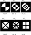
- the UV light sources used for curing printing plates typically emit divergent radiation, meaning the light that enters the plate through the mask openings diverges inside the plate in the shape of cones. A longer distance for the light to travel between plate surface and floor level leads to wider cones. With greater distance between plate floor level and print surface level, the marks on the floor become less visible later when the plate is processed. The elevation of the marks from the floor level 1910 to the non-printing level 1920 is not a sharp transition but a smooth ascent causing a structure with only little contrast. Consequently, marks, letters and barcodes on corrugated plates generally need to be bigger compared to marks on flexo plates to have a similar visibility to the human eye. Thus, it is advantageous to use alignment marks that have larger solid areas instead of crosshairs having thin lines.
- Fig. 6A to 6F show non-limiting examples of such advantageous alignment marks 2400, 2410, 2420, 2430, 2440, and 2450.
- the floor elevation is created by UV exposure of the polymer sheet through the LAMs (or a film) on the plate's front side, which will be the printing side after complete processing of the plate.
- the amount of UV light received determines the floor elevation of cured polymer on the PE foil.
- the size of the mask openings in turn, define the amount of UV light that can enter the plate. Therefore, the precision of the mask openings directly affects the precision of the floor elevation in the plate.
- microline patterns preferably oriented in the imaging direction of the LAMs (the direction of travel of the imager relative to the LAMs layer during an imaging step).
- microline patterns preferably oriented in the imaging direction of the LAMs (the direction of travel of the imager relative to the LAMs layer during an imaging step).
- microstructures refers to non-printing structures, which may be in the form of microdots (i.e. approximately circular) or microlines (also referred to herein as "line patterns” or “linear structures”).
- line patterns also referred to herein as "line patterns” or “linear structures”
- microstructures may also be used to refer to the mask openings that lead to the formation of microstructures on the plate, or the imaging information used by the imager to form the mask openings.
- a switching event is defined as an on-off switch of the imaging beam (e.g. laser).
- the switching time does not affect the imaging speed for linear mask openings as much as the switching time affects dot-shaped mask openings, as dot-shaped openings usually comprise clusters of several imaging pixels and require more switching events.
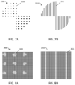
- FIGS. 7A and 7B show the mask openings for a registration mark made from conventional pixel clusters 2501.
- FIG. 7B the same registration mark is shown with the suggested pattern of lines 2511.
- the total number of imaging pixels used for the mask openings is nearly identical for both alignment marks, but for the mark in FIG. 7A , many more switching events occur.
- the line pattern also offers better definition of the outline of the crosshair, because it does not depend on fixed grid positions as much as patterns based on pixel clusters do.
- the two degrees of freedom for varying the opening of the LAMs include: the total number of pixels in the clusters; and the distance of the clusters from one another.
- the equivalent for these two degrees of freedom include the width of the line and the distance between the lines.
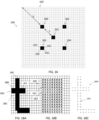
- FIG. 8A shows a screen style grid of 30 x 30 cells.
- Each cell represents a pixel in the image file used for ablating the LAMs.
- the tile comprises nine pixelclusters 2601, each having 10 ablated pixels.
- 90 pixels out of the 900 of the 30 x 30 cell matrix are mask openings that allow UV light to enter the plate and cure portions of the plate floor.
- a determination of alignment may be made by a human viewer observing the image on the display, or automatically using machine vision system 1537.
- the means 1524 for adjusting the position of the plate or plate portion bearing the micro alignment mark until it is disposed in the desired alignment position may comprise a human operator or a machine, such as an arm of a robotic handling system, and a machine positioner may be interactively controlled by a human or by a machine.
- a human operator controlling position of the plate (directly or via control of a machine positioner) may stop adjusting the plate position once the human operator detects the characteristic illumination on the display 1522.
- a machine positioner may be controlled by a controller 1526 programmed to stop adjustment of the plate upon receipt of a signal from the machine vision system 1537 that the plate is aligned.
- the plate positioner may move the plate relative to a substrate 1502 on which the plate is disposed, move the entire substrate 1502 relative to the LED ring, or a combination thereof.
- an exemplary method for orienting a plate relative to a workstation may include providing a ring of LEDs disposed above a surface of the plate, illuminating the ring of LEDs, and placing a plate as described herein having an isolated micro alignment mark on the substrate while observing light reflected by the plate from the illuminated ring of LEDs, such as using a camera viewing the reflection through optional optics.
- a user may adjust the location of the plate until the characteristic illumination pattern of the micro alignment mark by the ring of illuminated LEDs is observed that signifies that the micro alignment mark is centered relative to the LED ring.
- non-printing indicia may be formed above or below the plate floor, such as in the form of characters or codes readable by a human operator or machine vision system, and these characters or codes may be formed using micro dots.
- superimposing a homogenous pattern of micro dots on at least some types of characters may result in different elevation levels in different portions of the character. For example, referring now to the alphanumeric character 1800 depicted FIG.
- the elevated spots on the floor formed by each supercell may be arranged in lines and rows that form alphanumeric characters or codes with a constant elevation level. Due to the padding around the microdot clusters, the supercells avoid amplification from neighboring supercells that may otherwise form higher elevation levels if formed using different structures. Independently from the number and arrangement of supercells that form the indicia, the elevation level may thus be relatively constant for each dot formed by a supercell.
- FIGS. 18A-C depicts the translation of a letter "t" 1800 in FIG. 18A to a digital set 1810 of "on" (“1") pixels 1812 and "off" (“0") pixels 1811 in FIG. 18B to the arrangement 1820 of supercells 1822 corresponding to the "on” pixels in FIG. 18C , in accordance with the described method.
- indicia formed by dots 1922 disposed on plate 1920 define micro lenses capable of focusing light 1912 from a source 1910 located above the printing side of the plate to form a projected image 1932 on an opaque surface 1930 spaced a distance Z (e.g. 2- 8 mm) from the back side of the plate.
- Z e.g. 2- 8 mm
- the characters as viewed on the surface 1930 will be in the same orientation (but magnified) as the indicia as viewed from the front of the plate.
- FIG. 11D wherein alphanumeric characters viewed directly from the back of the plate will be a mirror image of the indicia as viewed from the front of the plate, the characters as viewed on the surface 1930 will be in the same orientation (but magnified) as the indicia as viewed from the front of the plate.
- FIG. 11D wherein alphanumeric characters viewed directly from the back of the plate will be a mirror image of the indicia as viewed from the front of the plate, the characters as viewed on
- 19 depicts the projected image 1932 in side view as having a height above the surface, this is for illustration only, as the image will be disposed on the (e.g. plane) defined by the surface, not above the surface, as will be well understood by one of skill in the art.
- the foregoing describes a modification to non-printed indicia that converts the inter-connected pattern structures into individual dots on the plate floor, which dots, when illuminated from the plate's printing side, give a clearly recognizable spot pattern of reflected light.
- the combination of all reflecting dots creates a pattern akin to zodiacal signs that can be easily recognized and decoded.
- the patterns can also be conceptualized as being akin to braille letters.
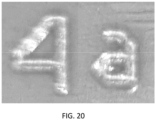
- FIG. 20 shows exemplary non-printing features of some of the earlier approaches described in the background section, which result in non-printing indicia that define solid interrelated structures. These structures may need to be illuminated from optimal directions to recognize them clearly.
- non-printing features have improved visibility when formed from single microdots instead of solid interrelated structures.
- these non-printing microdots on the plate floor function as a lens that concentrates light rays 301B, which propagate towards the top side of the polymer plate 100.
- the non-structured plate floor acts like a mirror and reflected light rays leave the plate without being substantially altered in their common direction.
- incoming light rays on the left side are concentrated by the non-printing polymer dot 102 on the other side of the plate floor on the dimensionally stable foil 105.
- the reflected rays that leave the plate have altered angular relationships.
- Scattering effects may also play a role, but the claimed invention is not limited to any particular physical mechanism for producing the observed effects relating to the claimed apparatus, systems, and/or methods.
- Those observed effects include a boundary behavior (e.g. transmission, reflection, and/or refraction) of radiation (e.g. light) applied to the isolated dots that is detectably different than the boundary behavior of the same radiation applied at a same angle on an area of the plate floor not having such an isolated dot.
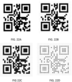
- FIG. 22A depicts a schematic example of a 21 x 21 matrix QR-code, equivalent to a 441-bit code, made from interrelated structures. Black areas in the drawing represent elevated structures, whereas white areas represent the floor level of the plate.
- FIG. 22B depicts a schematic example of the same QR-code of FIG. 22A , but with a visible grid that determines the possible positions of the elevated and non-elevated structures that embody the code. These positions are akin to pixels or bits of the code.
- FIG. 22B shows the same code and grid of FIG. 22B , but with the resolution of the grid doubled.
- FIG. 22D depicts the same QR code of FIGS. 22A-C with elevated details deleted in every other row and column (e.g.
- FIG. 23 depicts the exemplary code in which each individual dot of the code pattern is replaced by a matrix of image file pixel clusters, arranged in the supercell pattern 1600 depicted in FIG. 16 .
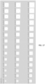
- FIG. 24 shows a photograph of the resulting, non-printing QR code pattern of FIG. 23 as formed on the floor of a DPR 045 plate.
- Fig. 25 shows the mask opening pixels of a supercell with respect to their position on the image file grid, with dimensions B, C, and D as described herein later.
- FIGS. 27 shows the result of a depth analysis using a confocal microscope of the microdots depicted in FIG. 26 on a DPR 045 Plate.
- Maintaining a preferred distance between the supercell positions in the mask grows individual dots without building the interconnected structures such as those depicted in Fig. 20 .
- the distance between the supercells is dependent on the type of polymer, the plate thickness, and the properties of the UV exposure radiation, including but not limited to irradiance, angular distribution of the propagating light rays, and wavelength composition of the light.
- the floor level is at a level of 50% of the cured plate thickness measured from the plate's non-printing back side while the non-printing elevated structures preferably do not exceed 20% of the total plate thickness above the floor in order to avoid printing.
- Exemplary measured elevation levels for the dot structures on a DPR 045 Plate between 40 and 55 ⁇ m are depicted in FIGS. 26 and 27 .
- the elevation level depends on boundary conditions such as plate type, exposure parameters, and the pattern of pixel clusters in the mask.
- elevation levels of the individual dots preferably range between 30 and 100 ⁇ m, more preferably between 40 and 80 ⁇ m.
- another advantage of using isolated dot structures rather than interconnected structures is that the dot structures have an overall lower elevation level.
- Minimizing height of the non-printing indicia structures above the plate floor is beneficial, because the less distance between the printing top surface and the tips of the highest non-printing structure elevations on the floor, the more likely the non-printing structures may experience undesired inking.
- the lower elevation provided by the isolated dot structures as described herein also greatly reduces the likeliness of unwanted printing as compared to other methods.
- the desired distance from the printing height and the size of the individual dots limit the number of dots per surface unit, which in turn also limits the amount of information that can be stored in a code on the plate floor. This limitation can be expressed in the number of dots respectively addressable using the unit measure "Bits per cm 2 .” For a common DRP 045 Plate developed under typical state of the art conditions, this parameter is approximately 80 Bit/cm 2 . Therefore, exemplary calculations for creating non-printing codes or alphanumeric signs for the non-printing image file start with the size requirements of the supercell in the light of the plate type and exposure unit. To make these calculations simple it is advantageous to have a library of supercells available for a given UV exposure system and various plate types and plate thickness.
- An exemplary library for supercells such as depicted in FIG. 25 contain characterizing information about the supercell types.
- Each supercell has a first number A of exposed pixel clusters, each exposed pixel cluster comprising a second number B of exposed pixels, the exposed pixel clusters are spaced apart from one another by a third number C of unexposed pixels, and finally a padding between the boundary of the supercell and a closest exposed pixel cluster is defined by a fourth number D of unexposed pixels.
- A, BAs depicted in FIG. 25 the black pixels represent mask openings while white pixels stand for absence of mask openings. TABLE 1 below gives some examples from an exemplary library of different supercell types for different plate types and for 4000 DPI image file resolution.
- the number of pixels of the supercells in one dimension can be calculated by Formula (1), below: 3 ⁇ B / 2 + 2 ⁇ C + 2 ⁇ D
- This resulting size of the pixel is the absolute dimensions of the supercell in one direction.
- the first supercell in TABLE 1 has a size of 86 x 86 pixels of the image file resolution.
- B/2 is not the exact value because the pixel cluster might have a different number of pixels in horizontal direction compared to the number of pixels in vertical direction. In this case adjustments must be made according to the shape of the pixel cluster.
- each pixel has 6.35 ⁇ m in the lateral direction, so the calculated lateral dimensions of the supercell for the DPR 045 in FIG. 1 is equivalent to 0.5461 x 0.5461 mm 2 in accordance with Formula 1.
- Type 1 supercells The information in TABLE 1 referring to supercells that will create interconnected structures is contained in the column titled "Type 1 Supercell size" and such supercells are referred to herein below as Type 1 supercells.
- an additional padding of 0.5 times the length of the Type 1 supercell must be added on each side of the supercell. This quadruples the size of the supercell.
- the supercell with additional padding will be called a Type 2 supercell herein below. Therefore, the space needed for a single Type 2 supercell corresponding to the Type 1 supercell referenced in TABLE 1 is increased to 1.0922 x 1.0922 mm 2 .
- the resulting dimension of a 21 X 21 Bit wide QR code as depicted in FIG. 24 on a DPR 045 Plate @ 4000 DPI image file resolution is about 22.9 x 22.9 mm, with the number of elevated dots that can be placed within one cm 2 being approximately 83.
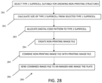
- An exemplary method of implementing patterns of non-printing code on the plate floor includes the steps outlined in flowchart 280 depicted schematically in FIG. 28 .
- the method includes in step 281, selecting from a library a Type 1 supercell containing a pattern of mask openings suitable for growing non-printing structures on the plate to be produced.
- the size of the Type 2 supercell is calculated from the dimension of the selected Type 1 supercell.
- the bits of a digital code pattern are allocated to a matrix of individual cells that are equivalent to the size of the calculated Type 2 supercell.
- a non-printing image file is created for imaging the mask by combining the bit information of the digital code pattern with the pixel clusters of the Type 2 supercell in order to cure the photopolymer plate.
- the non-printing image file comprising the digital code pattern supercell is combined with another image file comprising image information of the content to be printed, optionally (preferably but not necessarily) in a way that the elevated content of the non-printing image is located in the non-printing areas of the printing image.
- the combined image file is sent to an imager and the photopolymer plate is imaged. It should be understood that the size of the Type 2 supercell may be precalculated from suitable Type 1 supercells, such that the method does not need to include a specific calculation step.
- the image file resolution is typically matched to the grid determined by the size of the Type 2 supercell.
- fine tuning can be made by adjusting the thickness of the padding around the Type 1 supercell.
- the plate floor can also be exposed through the mask in a way that sunken structures are formed.
- sunken structures are formed.
- all features described in this document can also be realized in a reverse way as sunken instead of elevated dots, or as a combination of sunken and elevated dots.
- a grid of Type 1 supercells may be combined in a disjunction step with the image file containing the printing details. This creates an elevated floor in the UV curing step in all portions of the plate that do not comprise printing details.
- NAND NOT AND
- some individual Type 1 supercells are turned off at the places where sunken dots are needed in accordance with the image file of the non-printing details.
- FIGS. 30A-30D and 31A-31D Exemplary conjunction (AND) and disjunction (OR) operations are illustrated in FIGS. 30A-30D and 31A-31D , in which black pixels correspond to openings to be formed in the mask.
- FIG. 30A depicts an image file corresponding to a non-printing lowercase letter "t"
- FIG. 30B depicts a matrix of supercells (depicted as Type 2 but may be Type 1).
- FIG. 30C shows FIGS. 30A and 30B superimposed on one another at desired positions, with FIG. 30D showing a resulting image file formed by a logical conjunction operation, in which only the supercells that overlap with the non-printing image information (i.e. in the form of the letter "t") remain.
- the resulting pixels are imaged only if they are found in both the non-printing image information (e.g. FIG. 30A ) AND in the matrix of supercells (e.g. 30B).
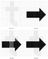
- FIG. 31A illustrates a non-printing image represented by non-printing supercells as described herein (i.e. identical to FIG. 30D , as produced by the conjunction operation).
- FIG. 31B illustrates a printing image in the form of an arrow.
- FIG. 31C illustrates the superimposition of 31A and 31B, and
- FIG. 31D shows the resulting image information as imaged on the mask.
- the disjunction step may be performed in an image file when executed in a computer or it may be directly executed on the LAMs layer by sequentially imaging both image files (printing and non-printing) onto the same plate.
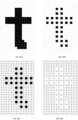
- FIGS. 32A-32D An example of a method for forming sunken structures by turning off selected supercells is illustrated in FIGS. 32A-32D.
- FIG. 32A depicts a lowercase letter "t" to be represented in non-printing characters.
- the letter "t” is converted into a "dotted” shape (i.e. every alternate pixel is turned “off") in FIG. 32B , and the "dotted "t” is then overlaid over the Type 1 supercell matrix depicted in FIG. 32C.
- FIG. 32A depicts a lowercase letter "t" to be represented in non-printing characters.
- 32D illustrates the resulting supercell matrix from a step in which each "positive" supercell corresponding to the "dotted t" turns “off” the entire Type 1 cell on which it is overlaid.
- This can be considered a "disjunctive" NAND (NOT AND) step in which the pixels as contained in FIG. 32B or 32C are both turned off if the dot AND the Type 1 supercell are overlapping when the files are superimposed.
- the pattern of elevated dots may also be used for the formation of processing marks (i.e. marks used for alignment, registration, or some other process-workflow-related purposes), such as alignment marks of the type discussed herein above.
- processing marks i.e. marks used for alignment, registration, or some other process-workflow-related purposes
- a CCD camera of a mobile phone is used for reading the dotted code information.
- An app on the phone converts the coded information of the dot-shaped structure back into alphanumeric signs and displays the information to the user. This allows easy identification of the correct plate in a plate storage, e.g. for a redo job by the user.
- a camera mounted on a XY-cutting table may be moved over the portions of the plate where the non-printing code is located to read cutting information implemented in the code.
- the code patch may contain information that points towards a server address.
- further details are stored in a computer file at a server accessible to the mobile phone or another reading device over a network, such as over a global computer network, or via WLAN, LAN, or other network technologies.
- This foregoing systems and methods may also be used to store information about the printing plates usage such as:
- Such information improves knowledge about printing plate wear before mounting the plate on a press and may facilitate decision making as to when to order a new plate.
- Material elevations on a substrate acting as reflecting points for incoming light may also be applicable to applications other than as embodied in photopolymer printing plates.
- Another use case includes providing printing elevations with clear paint on transparent foils. Such printed elevations are essentially invisible under daylight conditions, but become visible when the foil is illuminated by a point light source, such as an LED.
- An additional foil may be laminated onto the foil printed with the dots as a protective layer to make the printed dots more rugged.
- Optical-property-altering dots may also be applied by removing material from a surface, such as, for example, by etching, grinding, drilling, embossing, thermoforming and any other method of material processing known in the art. The use of such process may enable use in connection with a wide variety of materials other than photopolymer, such as glass or metal. Aspects of the invention are therefore not limited to any particular materials of construction or any particular method or system for forming the dot-based indicia.
- such dot-based indicia may be read based on the differences in optical properties (i.e. boundary properties) of the isolated dots relative to non-dot areas of the surface in the presence of applied light.
- the differences in optical properties may be detectable and readable by the human eye, or in preferred implementations, machine-readable.
- Preferred implementations include the use of a camera (such as in a mobile device) to, for example, read a machine-readable 1- or 2-dimensional code (e.g.
- QR code or barcode formed by dots that may be relatively less perceptible to the naked human eye than, for example, printed content, but that are clearly distinguishable when captured an in image taken by a camera that may be more sensitive to differences in optical properties or that may capture the image in conjunction with the use of applied light (i.e. incident light from a flash, or light from one or more other light sources reflecting, refracting, and/or transmitting light from or through the isolated dots and the surrounding surface).
- applied light i.e. incident light from a flash, or light from one or more other light sources reflecting, refracting, and/or transmitting light from or through the isolated dots and the surrounding surface.
- the process of communicating information using the isolated dots may further comprise the one or more processors translating the information embodied by the pattern of isolated dots and read by the reader into one or more instructions readable by a machine or into alphanumeric information readable by a human, which information may be usable for any of the purposes as described herein, generally. Implementations are not limited to those associated with a printing workflow, and the machine readable instructions may include any instruction readable by any machine or processor to cause the machine or the processor to instruct another machine connected to the processor to perform any act related to the article marked with the dot pattern.
Landscapes
- Physics & Mathematics (AREA)
- General Physics & Mathematics (AREA)
- Engineering & Computer Science (AREA)
- Multimedia (AREA)
- Manufacture Or Reproduction Of Printing Formes (AREA)
Claims (15)
- Ein Verfahren zum Platzieren von nichtdruckenden Bildinformationen auf einem Grund- bzw. Boden (floor) einer flexographischen Photopolymer-Druckplatte bzw. Flexodruck-Photopolymerplatte, wobei das Verfahren Folgendes umfasst: Bilden eines oder einer Reihe von isolierten nichtdruckenden Punkten (102), die den nichtdruckenden Bildinformationen entsprechen, wobei jeder Punkt in dem einen oder der Reihe von isolierten Punkten (1902, 2002) eine nichtdruckende Erhebung über dem Plattenboden (1901) aufweist oder unter dem Plattenboden (2001) versenkt ist, wobei die Reihe von isolierten Punkten ein oder mehrere Muster bildet, die ein oder mehrere alphanumerische Zeichen (1800), digitale Codes (212) oder Verarbeitungsmarkierungen (1512) darstellen, wobei das Verfahren Folgendes umfasst: Anordnen einer Maske (1904, 2004) auf der Photopolymerplatte (1900, 2000) in einem ungehärteten Zustand, Bebildern (imaging) der Maske, um eine bebilderte Maske gemäß einer Bilddatei zu bilden, die maschinenlesbare Anweisungen umfasst, die zumindest teilweise auf den nichtdruckenden Bildinformationen basieren, Härten des Photopolymers mit aktinischer Strahlung durch die Maske hindurch und Entfernen von ungehärtetem Polymer,
dadurch gekennzeichnet, dass
jeder isolierte nichtdruckende Punkt auf der Platte dem Vorhandensein einer Superzelle (1600) entspricht, die einen Pixelcluster (1610-1614) von Öffnungen in der Maske umfasst, wobei der Pixelcluster (1610-1614) eines oder mehrere Pixel (1620-1623) umfasst, von denen jedes einer Maskenöffnung in der Maske und einem freiliegenden bzw. belichteten (exposed) Pixel auf der Platte entspricht. - Das Verfahren nach Anspruch 1, wobei die Superzelle (1600) unbelichtete Pixel umfasst, die eine Abwesenheit von Öffnungen in der Maske umfassen, die innerhalb einer Superzellenbegrenzung (1640) angeordnet ist.
- Das Verfahren nach Anspruch 1 oder 2, wobei jede Superzelle (1600) eine erste Anzahl (A) von belichteten Pixelclustern (1610-1614) umfasst, wobei jeder belichtete Pixelcluster eine zweite Anzahl (B) belichteter Pixel (1620-1623) umfasst, wobei die belichteten Pixelcluster voneinander beabstandet sind durch eine dritte Anzahl (C) von unbelichteten Pixeln und einer Auffüllung bzw. einen Abstand (padding) zwischen der Superzellenbegrenzung und dem nächstgelegenen belichteten Pixelcluster, das durch eine vierte Anzahl (D) nicht belichteter Pixel definiert ist.
- Das Verfahren nach Anspruch 3, wobei jede Superzelle (1600) fünf belichtete Pixelcluster (1610-1614) umfasst, die einen zentralen Pixelcluster (1612) und vier äußere Pixelcluster (1610, 1611, 1613, 1614) beinhalten, wobei jeder äußere Pixelcluster eine innerste Ecke aufweist, die diagonal von einer Ecke des zentralen Pixelclusters durch die dritte Anzahl (C) unbelichteter Pixel beabstandet ist, und wobei die vierte Anzahl (D) von Pixeln eine diagonale Anordnung von Pixeln von einer äußersten Ecke jedes äußeren Pixelclusters zu einer Ecke der Superzellenbegrenzung (1640) umfasst.
- Das Verfahren nach irgendeinem der Ansprüche von 1 bis 4, wobei das Positionieren der isolierten nichtdruckenden Punkte (1902) mit einer nichtdruckenden Erhebung über dem Plattenboden (1901) berechnet wird, indem eine nichtdruckende Bilddatei, die nichtdruckende Bildinformationen enthält, in einzelne Abschnitte segmentiert wird, die der Größe der Superzelle entsprechen, und indem jeder Abschnitt der nichtdruckenden Bilddatei-Informationen mit einer Superzelle durch Konjunktion (conjunction) kombiniert wird, um kombinierte nichtdruckende Bildinformationen zu bilden, insbesondere ferner umfassend das Kombinieren der resultierenden kombinierten nichtdruckenden Bildinformationen mit druckenden Bildinformationen durch Disjunktion (disjunction), vorzugsweise eine ODER-Operation.
- Das Verfahren nach irgendeinem der Ansprüche von 1 bis 4, wobei das Positionieren der isolierten nichtdruckenden Punkte (2002), die unter dem Plattenboden (2001) versenkt sind, berechnet wird, indem ein Gitter von Superzellen in einem Disjunktionsschritt mit einer Bilddatei, die Druckdetails umfasst, kombiniert wird, um den Boden in Abschnitten der Platte zu erzeugen, die keine Druckdetails umfassen, und indem, in einem weiteren Disjunktionsschritt, ausgewählte Superzellen in Übereinstimmung mit einer nichtdruckenden Bilddatei, die nichtdruckende Bildinformationen enthält, deaktiviert werden, um die nichtdruckenden Punkte zu erzeugen, die unter dem Plattenboden versenkt sind.
- Das Verfahren nach irgendeinem der Ansprüche 1 bis 6, ferner umfassend das Auswählen von Merkmalen für die Superzelle auf der Grundlage des Plattentyps, der Plattendicke, der Härtungsparameter der aktinischen Strahlung und der Auflösung der Bilddatei.
- Das Verfahren nach Anspruch 7, Speichern einer Vielzahl optimaler Superzellen-Merkmale als ein Satz maschinenlesbarer Anweisungen in einer Computerspeicherbibliothek, wobei der Schritt des Auswählens Folgendes umfasst: Auswählen der Merkmale für die Superzelle aus der Computerspeicherbibliothek mit einem Computer, und Bilden der maschinenlesbaren Anweisungen in der Bilddatei entsprechend der nicht druckbaren Bildinformation auf der Grundlage der ausgewählten Merkmale.
- Das Verfahren nach irgendeinem der vorstehenden Ansprüche, wobei die nichtdruckenden Kennzeichnungen (indicia) (1800) einen oder mehrere Kreuzungsbereiche umfassen, in denen ein erster Zeichen-Abschnitt (1801) einen zweiten Zeichen-Abschnitt (1804) kreuzt, wobei eine Erhebung des Kreuzungsbereichs der nichtdruckenden Kennzeichnungen dieselbe ist wie eine Erhebung eines kreuzungsfreien Bereichs (1802, 1803) der nichtdruckenden Kennzeichnungen.
- Das Verfahren nach irgendeinem der vorstehenden Ansprüche, wobei die Maske eine durch Laser ablatierbare Maske umfasst.
- Das Verfahren nach irgendeinem der vorstehenden Ansprüche, wobei die Maske einen lichtempfindlichen Film oder einen wärmeempfindlichen Film umfasst.
- Das Verfahren nach irgendeinem der vorstehenden Ansprüche, wobei die Verarbeitungs-Markierungen eine oder mehrere Markierungen umfassen, die für die Ausrichtung (1512), die Registrierung oder einen anderen prozessablaufbezogenen Zweck verwendet werden.
- Das Verfahren nach Anspruch 12, wobei die Verarbeitungs-Markierung eine isolierte Mikroausrichtungs-Markierung (1512) umfasst, die durch Überlagern eines sich wiederholenden Musters von durch die Pixelcluster definierten Mikrostrukturen über eine Vollpunktform gebildet wird.
- Ein Verfahren zum Ausrichten einer Druckplatte mit mindestens einer isolierten Mikroausrichtungs-Markierung, die durch den Prozess nach Anspruch 13 gebildet wird, wobei das Verfahren die folgenden Schritte umfasst:Bereitstellen eines Rings aus LEDs (1524), die so angeordnet sind, dass sie eine Oberfläche der Druckplatte (1510) beleuchten;Aufleuchten Lassen des LED-Rings;Bereitstellen der Druckplatte in einem Beleuchtungsfeld des LED-Rings, während das von der Druckplatte reflektierte Licht beobachtet wird;Anpassen einer Position der Platte, bis ein charakteristisches Beleuchtungsmuster der isolierten Mikroausrichtungs-Markierung durch den Ring aus aufleuchtenden LEDs beobachtet wird, was bedeutet, dass die isolierte Mikroausrichtungs-Markierung relativ zum LED-Ring zentriert ist.
- Ein nicht-flüchtiges computerlesbares Speichermedium mit darin gespeicherten Daten, die Anweisungen darstellen, um einen Bildgeber zu veranlassen, die Vielzahl von Superzellen nach irgendeinem der Ansprüche 1-13 abzubilden.
Priority Applications (3)
| Application Number | Priority Date | Filing Date | Title |
|---|---|---|---|
| EP25180515.6A EP4589386A3 (de) | 2021-11-01 | 2022-05-11 | System und verfahren zur dauerhaften markierung von flexoplatten mit isolierten mikrostrukturen und damit markierte platten |
| EP22809164.1A EP4399574A1 (de) | 2021-11-01 | 2022-10-31 | Systeme und verfahren zur dauerhaften markierung von flexoplatten mit isolierten mikrostrukturen und damit markierte platten |
| PCT/EP2022/080376 WO2023073232A1 (en) | 2021-11-01 | 2022-10-31 | Systems and processes for persistent marking of flexo plates with isolated microstructures and plates marked therewith |
Applications Claiming Priority (1)
| Application Number | Priority Date | Filing Date | Title |
|---|---|---|---|
| US202163274202P | 2021-11-01 | 2021-11-01 |
Related Child Applications (1)
| Application Number | Title | Priority Date | Filing Date |
|---|---|---|---|
| EP25180515.6A Division EP4589386A3 (de) | 2021-11-01 | 2022-05-11 | System und verfahren zur dauerhaften markierung von flexoplatten mit isolierten mikrostrukturen und damit markierte platten |
Publications (2)
| Publication Number | Publication Date |
|---|---|
| EP4174579A1 EP4174579A1 (de) | 2023-05-03 |
| EP4174579B1 true EP4174579B1 (de) | 2025-07-02 |
Family
ID=81603480
Family Applications (1)
| Application Number | Title | Priority Date | Filing Date |
|---|---|---|---|
| EP22172781.1A Active EP4174579B1 (de) | 2021-11-01 | 2022-05-11 | System und verfahren zum dauerhaften markieren von flexoplatten mit isolierten mikrostrukturen und damit markierte platten |
Country Status (2)
| Country | Link |
|---|---|
| EP (1) | EP4174579B1 (de) |
| CN (1) | CN118696276A (de) |
Family Cites Families (8)
| Publication number | Priority date | Publication date | Assignee | Title |
|---|---|---|---|---|
| GB2323664A (en) * | 1997-03-25 | 1998-09-30 | Dek Printing Machines Ltd | Viewing and imaging systems |
| US20050157347A1 (en) | 2004-01-21 | 2005-07-21 | Hans Dewitte | Relief plates, platemaking masters therefor, and methods for producing such plate making masters and plates |
| US9375916B2 (en) | 2010-06-18 | 2016-06-28 | Esko-Graphics Imaging Gmbh | Non-printing registration marks on a printing plate |
| US20120048133A1 (en) * | 2010-08-25 | 2012-03-01 | Burberry Mitchell S | Flexographic printing members |
| US10732507B2 (en) | 2015-10-26 | 2020-08-04 | Esko-Graphics Imaging Gmbh | Process and apparatus for controlled exposure of flexographic printing plates and adjusting the floor thereof |
| EP3984761B1 (de) | 2016-05-27 | 2025-10-15 | Esko Software BV | Verfahren für glattere tonale reaktion beim flexodruck |
| CN113330368B (zh) * | 2019-02-01 | 2024-11-29 | 埃斯科绘图成像有限责任公司 | 用于柔性印版的持久标识的系统和方法以及用其标识的印版 |
| WO2020221684A1 (en) * | 2019-04-30 | 2020-11-05 | Agfa Nv | Digital halftoning with spiral dots |
-
2022
- 2022-05-11 EP EP22172781.1A patent/EP4174579B1/de active Active
- 2022-10-31 CN CN202280073502.XA patent/CN118696276A/zh active Pending
Also Published As
| Publication number | Publication date |
|---|---|
| CN118696276A (zh) | 2024-09-24 |
| EP4174579A1 (de) | 2023-05-03 |
Similar Documents
| Publication | Publication Date | Title |
|---|---|---|
| US11724533B2 (en) | System and process for persistent marking of flexo plates and plates marked therewith | |
| US11878540B2 (en) | Flexographic printing plate with persistent markings | |
| CN113330368B (zh) | 用于柔性印版的持久标识的系统和方法以及用其标识的印版 | |
| CN114730141B (zh) | 用于柔印版的持久标记的系统和方法以及利用其标记的版 | |
| RU2384884C2 (ru) | Носитель данных с элементом защиты и способ его изготовления | |
| JP4570389B2 (ja) | レーザマーキングによる2次元コードの形成方法、及びレーザマーキング装置 | |
| EP3790741B1 (de) | Verfahren zur herstellung einer sichtbare und nicht druckbare information enthaltenden flexographiedruckplatte | |
| EP4589386A2 (de) | System und verfahren zur dauerhaften markierung von flexoplatten mit isolierten mikrostrukturen und damit markierte platten | |
| DE112021006128T5 (de) | System und Verfahren zum Nachverfolgen von Drucksystemmetriken und zur prädiktiven Überwachung eines Druckwerkzeugs | |
| KR20170129801A (ko) | 임프린트된 보안 특성을 제공하는 방법 | |
| WO2022112342A1 (en) | Printing plates with printing structures having multiple elevations and, systems and process for manufacture, and methods for use of the same | |
| EP4174579B1 (de) | System und verfahren zum dauerhaften markieren von flexoplatten mit isolierten mikrostrukturen und damit markierte platten | |
| JP4091359B2 (ja) | 二次元コードのマーキング方法及びそのマーキング装置 | |
| JP2026001302A (ja) | 情報識別方法および印刷物 | |
| JP2026001300A (ja) | 情報識別方法、包装材料および樹脂成形体 | |
| CN120548506A (zh) | 用于跟踪数字光敏聚合物印刷印版的生产工作流程信息的系统 | |
| JP2020536770A (ja) | 追跡用二次元コードを有する印刷版原版及び印刷版、並びにその使用システム |
Legal Events
| Date | Code | Title | Description |
|---|---|---|---|
| PUAI | Public reference made under article 153(3) epc to a published international application that has entered the european phase |
Free format text: ORIGINAL CODE: 0009012 |
|
| STAA | Information on the status of an ep patent application or granted ep patent |
Free format text: STATUS: THE APPLICATION HAS BEEN PUBLISHED |
|
| AK | Designated contracting states |
Kind code of ref document: A1 Designated state(s): AL AT BE BG CH CY CZ DE DK EE ES FI FR GB GR HR HU IE IS IT LI LT LU LV MC MK MT NL NO PL PT RO RS SE SI SK SM TR |
|
| STAA | Information on the status of an ep patent application or granted ep patent |
Free format text: STATUS: REQUEST FOR EXAMINATION WAS MADE |
|
| 17P | Request for examination filed |
Effective date: 20231102 |
|
| RBV | Designated contracting states (corrected) |
Designated state(s): AL AT BE BG CH CY CZ DE DK EE ES FI FR GB GR HR HU IE IS IT LI LT LU LV MC MK MT NL NO PL PT RO RS SE SI SK SM TR |
|
| GRAP | Despatch of communication of intention to grant a patent |
Free format text: ORIGINAL CODE: EPIDOSNIGR1 |
|
| STAA | Information on the status of an ep patent application or granted ep patent |
Free format text: STATUS: GRANT OF PATENT IS INTENDED |
|
| INTG | Intention to grant announced |
Effective date: 20241218 |
|
| GRAS | Grant fee paid |
Free format text: ORIGINAL CODE: EPIDOSNIGR3 |
|
| GRAA | (expected) grant |
Free format text: ORIGINAL CODE: 0009210 |
|
| STAA | Information on the status of an ep patent application or granted ep patent |
Free format text: STATUS: THE PATENT HAS BEEN GRANTED |
|
| AK | Designated contracting states |
Kind code of ref document: B1 Designated state(s): AL AT BE BG CH CY CZ DE DK EE ES FI FR GB GR HR HU IE IS IT LI LT LU LV MC MK MT NL NO PL PT RO RS SE SI SK SM TR |
|
| REG | Reference to a national code |
Ref country code: GB Ref legal event code: FG4D |
|
| REG | Reference to a national code |
Ref country code: CH Ref legal event code: EP |
|
| REG | Reference to a national code |
Ref country code: DE Ref legal event code: R096 Ref document number: 602022016705 Country of ref document: DE |
|
| REG | Reference to a national code |
Ref country code: IE Ref legal event code: FG4D |
|
| REG | Reference to a national code |
Ref country code: NL Ref legal event code: MP Effective date: 20250702 |
|
| PG25 | Lapsed in a contracting state [announced via postgrant information from national office to epo] |
Ref country code: PT Free format text: LAPSE BECAUSE OF FAILURE TO SUBMIT A TRANSLATION OF THE DESCRIPTION OR TO PAY THE FEE WITHIN THE PRESCRIBED TIME-LIMIT Effective date: 20251103 |
|
| PG25 | Lapsed in a contracting state [announced via postgrant information from national office to epo] |
Ref country code: NL Free format text: LAPSE BECAUSE OF FAILURE TO SUBMIT A TRANSLATION OF THE DESCRIPTION OR TO PAY THE FEE WITHIN THE PRESCRIBED TIME-LIMIT Effective date: 20250702 |
|
| REG | Reference to a national code |
Ref country code: AT Ref legal event code: MK05 Ref document number: 1809903 Country of ref document: AT Kind code of ref document: T Effective date: 20250702 |
|
| PG25 | Lapsed in a contracting state [announced via postgrant information from national office to epo] |
Ref country code: IS Free format text: LAPSE BECAUSE OF FAILURE TO SUBMIT A TRANSLATION OF THE DESCRIPTION OR TO PAY THE FEE WITHIN THE PRESCRIBED TIME-LIMIT Effective date: 20251102 |
|
| PG25 | Lapsed in a contracting state [announced via postgrant information from national office to epo] |
Ref country code: NO Free format text: LAPSE BECAUSE OF FAILURE TO SUBMIT A TRANSLATION OF THE DESCRIPTION OR TO PAY THE FEE WITHIN THE PRESCRIBED TIME-LIMIT Effective date: 20251002 |
|
| REG | Reference to a national code |
Ref country code: LT Ref legal event code: MG9D |
|
| PG25 | Lapsed in a contracting state [announced via postgrant information from national office to epo] |
Ref country code: AT Free format text: LAPSE BECAUSE OF FAILURE TO SUBMIT A TRANSLATION OF THE DESCRIPTION OR TO PAY THE FEE WITHIN THE PRESCRIBED TIME-LIMIT Effective date: 20250702 |
|
| PG25 | Lapsed in a contracting state [announced via postgrant information from national office to epo] |
Ref country code: FI Free format text: LAPSE BECAUSE OF FAILURE TO SUBMIT A TRANSLATION OF THE DESCRIPTION OR TO PAY THE FEE WITHIN THE PRESCRIBED TIME-LIMIT Effective date: 20250702 |
|
| PG25 | Lapsed in a contracting state [announced via postgrant information from national office to epo] |
Ref country code: HR Free format text: LAPSE BECAUSE OF FAILURE TO SUBMIT A TRANSLATION OF THE DESCRIPTION OR TO PAY THE FEE WITHIN THE PRESCRIBED TIME-LIMIT Effective date: 20250702 |
|
| PG25 | Lapsed in a contracting state [announced via postgrant information from national office to epo] |
Ref country code: GR Free format text: LAPSE BECAUSE OF FAILURE TO SUBMIT A TRANSLATION OF THE DESCRIPTION OR TO PAY THE FEE WITHIN THE PRESCRIBED TIME-LIMIT Effective date: 20251003 |
|
| PG25 | Lapsed in a contracting state [announced via postgrant information from national office to epo] |
Ref country code: SE Free format text: LAPSE BECAUSE OF FAILURE TO SUBMIT A TRANSLATION OF THE DESCRIPTION OR TO PAY THE FEE WITHIN THE PRESCRIBED TIME-LIMIT Effective date: 20250702 Ref country code: CZ Free format text: LAPSE BECAUSE OF FAILURE TO SUBMIT A TRANSLATION OF THE DESCRIPTION OR TO PAY THE FEE WITHIN THE PRESCRIBED TIME-LIMIT Effective date: 20250702 |
|
| PG25 | Lapsed in a contracting state [announced via postgrant information from national office to epo] |
Ref country code: LV Free format text: LAPSE BECAUSE OF FAILURE TO SUBMIT A TRANSLATION OF THE DESCRIPTION OR TO PAY THE FEE WITHIN THE PRESCRIBED TIME-LIMIT Effective date: 20250702 |
|
| PG25 | Lapsed in a contracting state [announced via postgrant information from national office to epo] |
Ref country code: BG Free format text: LAPSE BECAUSE OF FAILURE TO SUBMIT A TRANSLATION OF THE DESCRIPTION OR TO PAY THE FEE WITHIN THE PRESCRIBED TIME-LIMIT Effective date: 20250702 Ref country code: PL Free format text: LAPSE BECAUSE OF FAILURE TO SUBMIT A TRANSLATION OF THE DESCRIPTION OR TO PAY THE FEE WITHIN THE PRESCRIBED TIME-LIMIT Effective date: 20250702 |
|
| PG25 | Lapsed in a contracting state [announced via postgrant information from national office to epo] |
Ref country code: RS Free format text: LAPSE BECAUSE OF FAILURE TO SUBMIT A TRANSLATION OF THE DESCRIPTION OR TO PAY THE FEE WITHIN THE PRESCRIBED TIME-LIMIT Effective date: 20251002 |
|
| PG25 | Lapsed in a contracting state [announced via postgrant information from national office to epo] |
Ref country code: ES Free format text: LAPSE BECAUSE OF FAILURE TO SUBMIT A TRANSLATION OF THE DESCRIPTION OR TO PAY THE FEE WITHIN THE PRESCRIBED TIME-LIMIT Effective date: 20250702 |
|
| PG25 | Lapsed in a contracting state [announced via postgrant information from national office to epo] |
Ref country code: SM Free format text: LAPSE BECAUSE OF FAILURE TO SUBMIT A TRANSLATION OF THE DESCRIPTION OR TO PAY THE FEE WITHIN THE PRESCRIBED TIME-LIMIT Effective date: 20250702 |
|
| PG25 | Lapsed in a contracting state [announced via postgrant information from national office to epo] |
Ref country code: DK Free format text: LAPSE BECAUSE OF FAILURE TO SUBMIT A TRANSLATION OF THE DESCRIPTION OR TO PAY THE FEE WITHIN THE PRESCRIBED TIME-LIMIT Effective date: 20250702 |
|
| PG25 | Lapsed in a contracting state [announced via postgrant information from national office to epo] |
Ref country code: IT Free format text: LAPSE BECAUSE OF FAILURE TO SUBMIT A TRANSLATION OF THE DESCRIPTION OR TO PAY THE FEE WITHIN THE PRESCRIBED TIME-LIMIT Effective date: 20250702 |
|
| PG25 | Lapsed in a contracting state [announced via postgrant information from national office to epo] |
Ref country code: EE Free format text: LAPSE BECAUSE OF FAILURE TO SUBMIT A TRANSLATION OF THE DESCRIPTION OR TO PAY THE FEE WITHIN THE PRESCRIBED TIME-LIMIT Effective date: 20250702 Ref country code: SK Free format text: LAPSE BECAUSE OF FAILURE TO SUBMIT A TRANSLATION OF THE DESCRIPTION OR TO PAY THE FEE WITHIN THE PRESCRIBED TIME-LIMIT Effective date: 20250702 |