EP4174884A1 - Innovative struktur einer planaren elektromagnetischen komponente - Google Patents
Innovative struktur einer planaren elektromagnetischen komponente Download PDFInfo
- Publication number
- EP4174884A1 EP4174884A1 EP22202891.2A EP22202891A EP4174884A1 EP 4174884 A1 EP4174884 A1 EP 4174884A1 EP 22202891 A EP22202891 A EP 22202891A EP 4174884 A1 EP4174884 A1 EP 4174884A1
- Authority
- EP
- European Patent Office
- Prior art keywords
- turns
- primary
- layers
- vias
- winding
- Prior art date
- Legal status (The legal status is an assumption and is not a legal conclusion. Google has not performed a legal analysis and makes no representation as to the accuracy of the status listed.)
- Pending
Links
Images


Classifications
-
- H—ELECTRICITY
- H01—ELECTRIC ELEMENTS
- H01F—MAGNETS; INDUCTANCES; TRANSFORMERS; SELECTION OF MATERIALS FOR THEIR MAGNETIC PROPERTIES
- H01F27/00—Details of transformers or inductances, in general
- H01F27/28—Coils; Windings; Conductive connections
- H01F27/30—Fastening or clamping coils, windings, or parts thereof together; Fastening or mounting coils or windings on core, casing, or other support
-
- H—ELECTRICITY
- H01—ELECTRIC ELEMENTS
- H01F—MAGNETS; INDUCTANCES; TRANSFORMERS; SELECTION OF MATERIALS FOR THEIR MAGNETIC PROPERTIES
- H01F27/00—Details of transformers or inductances, in general
- H01F27/28—Coils; Windings; Conductive connections
- H01F27/2804—Printed windings
-
- H—ELECTRICITY
- H01—ELECTRIC ELEMENTS
- H01F—MAGNETS; INDUCTANCES; TRANSFORMERS; SELECTION OF MATERIALS FOR THEIR MAGNETIC PROPERTIES
- H01F27/00—Details of transformers or inductances, in general
- H01F27/28—Coils; Windings; Conductive connections
- H01F27/288—Shielding
-
- H—ELECTRICITY
- H01—ELECTRIC ELEMENTS
- H01F—MAGNETS; INDUCTANCES; TRANSFORMERS; SELECTION OF MATERIALS FOR THEIR MAGNETIC PROPERTIES
- H01F27/00—Details of transformers or inductances, in general
- H01F27/28—Coils; Windings; Conductive connections
- H01F27/29—Terminals; Tapping arrangements for signal inductances
-
- H—ELECTRICITY
- H01—ELECTRIC ELEMENTS
- H01F—MAGNETS; INDUCTANCES; TRANSFORMERS; SELECTION OF MATERIALS FOR THEIR MAGNETIC PROPERTIES
- H01F27/00—Details of transformers or inductances, in general
- H01F27/40—Structural association with built-in electric component, e.g. fuse
- H01F27/402—Association of measuring or protective means
-
- H—ELECTRICITY
- H01—ELECTRIC ELEMENTS
- H01F—MAGNETS; INDUCTANCES; TRANSFORMERS; SELECTION OF MATERIALS FOR THEIR MAGNETIC PROPERTIES
- H01F5/00—Coils
- H01F5/04—Arrangements of electric connections to coils, e.g. leads
- H01F2005/046—Details of formers and pin terminals related to mounting on printed circuits
-
- H—ELECTRICITY
- H01—ELECTRIC ELEMENTS
- H01F—MAGNETS; INDUCTANCES; TRANSFORMERS; SELECTION OF MATERIALS FOR THEIR MAGNETIC PROPERTIES
- H01F27/00—Details of transformers or inductances, in general
- H01F27/06—Mounting, supporting or suspending transformers, reactors or choke coils not being of the signal type
- H01F2027/065—Mounting on printed circuit boards
-
- H—ELECTRICITY
- H01—ELECTRIC ELEMENTS
- H01F—MAGNETS; INDUCTANCES; TRANSFORMERS; SELECTION OF MATERIALS FOR THEIR MAGNETIC PROPERTIES
- H01F27/00—Details of transformers or inductances, in general
- H01F27/28—Coils; Windings; Conductive connections
- H01F27/2804—Printed windings
- H01F2027/2809—Printed windings on stacked layers
-
- H—ELECTRICITY
- H01—ELECTRIC ELEMENTS
- H01F—MAGNETS; INDUCTANCES; TRANSFORMERS; SELECTION OF MATERIALS FOR THEIR MAGNETIC PROPERTIES
- H01F27/00—Details of transformers or inductances, in general
- H01F27/28—Coils; Windings; Conductive connections
- H01F27/2804—Printed windings
- H01F2027/2819—Planar transformers with printed windings, e.g. surrounded by two cores and to be mounted on printed circuit
-
- H—ELECTRICITY
- H01—ELECTRIC ELEMENTS
- H01F—MAGNETS; INDUCTANCES; TRANSFORMERS; SELECTION OF MATERIALS FOR THEIR MAGNETIC PROPERTIES
- H01F27/00—Details of transformers or inductances, in general
- H01F27/34—Special means for preventing or reducing unwanted electric or magnetic effects, e.g. no-load losses, reactive currents, harmonics, oscillations, leakage fields
- H01F27/346—Preventing or reducing leakage fields
-
- H—ELECTRICITY
- H01—ELECTRIC ELEMENTS
- H01F—MAGNETS; INDUCTANCES; TRANSFORMERS; SELECTION OF MATERIALS FOR THEIR MAGNETIC PROPERTIES
- H01F3/00—Cores, Yokes, or armatures
- H01F3/10—Composite arrangements of magnetic circuits
- H01F3/14—Constrictions; Gaps, e.g. air-gaps
Definitions
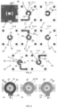
- FIG. 1 schematically represents an example of implementation of a planar magnetic component 5 according to the state of the art.
- This component 5 consists of an electrical circuit 6, consisting of one or more windings 7, themselves consisting of one or more turns (7-1, 7-2, 7-3, 7-4). These windings aim to produce a magnetic field. This field can be used for energy storage (inductance) or for transfer (transformer).
- Component 5 comprises a ferromagnetic core 8, which channels the magnetic field. We then speak of a magnetic circuit.
- This core 8 can be made of several materials depending on the target application (power/frequency/price/size/performance).
- the core 8 may comprise an air gap 9, a small air space in the circuit, extending parallel to the plane of the circuit.
- the circulation of the current in the electrical circuit generates losses in the same way as the circulation of the magnetic field in the magnetic circuit.
- the losses in the two elements are respectively called copper losses and iron losses. These losses are interrelated. It is therefore desirable to optimize the dimensions of each of the elements according to the application in order to maximize the performance of the assembly.
- the invention aims to overcome all or part of the problems mentioned above by proposing a transformer comprising an innovative electromagnetic component structure making it possible to optimize the performance of the transformer by minimizing the losses, by improving the integration of the PCB (abbreviation of Printed Circuit Board, for printed circuit) by limiting vias on the periphery of components, by limiting parasitic inductances and improving couplings.
- PCB abbreviation of Printed Circuit Board, for printed circuit
- the ferromagnetic core comprises an air gap extending along a second axis substantially perpendicular to the first plane.
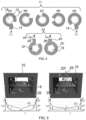
- the transformer 10 comprises a secondary circuit 21 comprising a secondary winding 22 of N2 turns of a conductive electric wire, the secondary winding 22 extending from a secondary input terminal 23 towards a secondary output terminal 24 (N1 and N2 each being a whole number greater than or equal to 1).
- the transformer 10 comprises a printed circuit 15 (broken down in the figure into several layers) extending along a first plane 16, and comprising a plurality of layers 17-1, 17-2, 17-3, 17-4, 17-5, 17-6, 17-7 superposed together and forming an opening 18 through the first plane 16 around a first axis Z1 and defining a perimeter 19.
- Each of the N1 turns and the N2 turns wraps, from a first via of the plurality of vias 27, partially around the plurality of vias 27 forming an arc of a circle 28 per layer, towards a second via of the plurality of vias 27
- the turn of the winding (primary or secondary) is not a complete turn, the turn is only 360° around the opening 18.
- a few vias per layer do not are not surrounded by said tower.
- the central arrangement of the vias brings great flexibility to the positioning of the layers which can be intercalated with respect to each other, and therefore to the positioning of the turns of the primary winding and of the secondary winding.
- vias in the center of the magnetic component allows a simplified realization of the various windings. For this, it is possible to reproduce an elementary winding on each of the layers (b) in order to produce the desired winding. Only one turn is made per PCB layer. The passage between the different layers takes place via the central vias 27. One or more vias can be used for this purpose depending on the desired current in the windings and the size of the core 25 (and its central part 26).
- FIG 4 schematically represents an example of implementation of the primary 12 and secondary 22 windings of a transformer 10 according to the invention. More specifically, the output winding is incorporated within the crown of central vias 27. In order to interleave the primary and secondary windings, here too the vias allowing the interconnections between the layers 17 are also interleaved.
- the turns of the secondary winding can each be inserted between two turns of the primary winding and/or between a turn of the primary winding and a turn of the secondary winding.
- This configuration is advantageous for a transformer since it allows better integration and facilitates the implementation of shielding in order to further limit the impact of proximity effects (and only in the case where the component has an air gap).
- the minimization of the induction at the level of the interconnections allows the reduction of the losses.
- the ferromagnetic core 25 comprises an air gap 29 extending along a second axis Z2 substantially perpendicular to the first plane 16.
- the use of a vertical air gap 29 is made possible by machining existing cores or material bully.
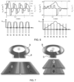
- planar cores most often have an air gap arranged on the central leg which causes the field to radiate in a direction parallel to the planar windings (see illustration on the left).
- the configuration on the left of the figure represents a central copper conductor subject to leakage fields emanating from the two air gaps in the magnetic core.
- the current densities are concentrated on the edges of the conductor which decreases the efficiency of the solution.
- the magnetic field propagates in the core.
- the field lines radiate around the air gap and these field lines tend to concentrate the currents flowing in the conductor outwards to such an extent that the current flows only on the outside, where the lines of field concentrate it. In other words, only a small part of the conductor is actually used.
- the leakage fields arrive perpendicular to the conductor, which allows the current density and therefore the losses to be reduced. More precisely, in a vertical arrangement, the field radiates perpendicularly (see illustration on the right), which reduces the effects of proximity to the core and therefore reduces the concentration of current, at the ends, in the electrical circuit. The currents are concentrated on the surface and the entire conductor is used. This results in a positive impact on radiation. Thus, the resistance of the winding is decreased.
- FIG. 6 schematically represents the induction between the conductors according to the alternation of the turns of the primary and secondary windings.
- the conductors in a planar transformer are shown.
- the layers annotated P1 represent the primary conductors while the layers annotated S1 represent the secondary conductors.
- the turns of the primary winding and the turns of the secondary winding are arranged alternately, the choice of the alternation mode is facilitated according to the invention.
- the turns of the primary winding and the turns of the secondary winding follow one another, without any alternation between the primary and secondary windings.
- the profile of the theoretical induction is given (H).
- FIG 7 schematically represents the homogenization of the current density in the input and output terminals of the primary and secondary windings arranged according to an embodiment of the invention.
- This representation is based on an illustration from the Schafer 2018 publication Optimal Design of Highly Efficient and Highly Compact PCB Winding Inductors.
- the input terminals 13, 23 are superimposed on the output terminals 14, 24 along a third axis Z3 substantially perpendicular to the first plane 16, as can be seen in the upper part on the right of the figure. This makes it possible to avoid field concentration phenomena between the two planes. With the terminals positioned in two different parallel planes, the current is more distributed throughout the plane and not just concentrated in the middle of a single plane.
- the lower part of the figure represents the results of a finite element simulation of the current density with adjacent terminals (on the left of the figure) and superposed terminals according to the invention (on the right of the figure).
- the implementation of the solution is profitable if it makes it possible to reduce total losses.
- the reduction in the equivalent resistance of the conductors is a factor to be taken into account. Limiting this resistance makes it possible to facilitate primary resonance and therefore soft switching. In this particular case, it will therefore also be necessary to take into account the gain provided by this operation on the sizing of the magnetic.
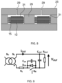
- FIG. 9 schematically represents a classic electrical diagram of a synchronous rectification.
- the transformer ideal coupler
- Rs represents the parasitic series resistance of the secondary winding and of the routing
- QR the synchronous rectification transistor
- DQR and CQR the parasitic components associated with this transistor.
- Cout and Rout represent the output capacity of the converter and the load respectively.
- FIG 10 schematically represents the optimization of the output terminals for synchronous rectification according to the invention.
- the winding can be done using every other group of vias.
- By optimizing the terminals of the transformer it is possible to improve the integration of the secondary in order to minimize the losses at the level of the synchronous rectification.
- a lowering of the voltage is carried out between the primary and the secondary. This results in a voltage at the secondary lower than at the primary. It also means stronger secondary currents.
- This improvement leads to a reduction in the resistance R s and in the parasitic inductances at the secondary. In addition, it allows an easier increase in the number of transistors in the synchronous rectification, which makes it possible to reduce the losses all the more.
Landscapes
- Engineering & Computer Science (AREA)
- Power Engineering (AREA)
- Chemical & Material Sciences (AREA)
- Composite Materials (AREA)
- Coils Or Transformers For Communication (AREA)
- Coils Of Transformers For General Uses (AREA)
- Regulation Of General Use Transformers (AREA)
Applications Claiming Priority (1)
| Application Number | Priority Date | Filing Date | Title |
|---|---|---|---|
| FR2111347A FR3128573A1 (fr) | 2021-10-26 | 2021-10-26 | Structure innovante de composant électromagnétique planar |
Publications (1)
| Publication Number | Publication Date |
|---|---|
| EP4174884A1 true EP4174884A1 (de) | 2023-05-03 |
Family
ID=79018941
Family Applications (1)
| Application Number | Title | Priority Date | Filing Date |
|---|---|---|---|
| EP22202891.2A Pending EP4174884A1 (de) | 2021-10-26 | 2022-10-21 | Innovative struktur einer planaren elektromagnetischen komponente |
Country Status (7)
| Country | Link |
|---|---|
| US (1) | US12586708B2 (de) |
| EP (1) | EP4174884A1 (de) |
| JP (1) | JP2023064716A (de) |
| KR (1) | KR20230059759A (de) |
| CN (1) | CN116031051A (de) |
| CA (1) | CA3179766A1 (de) |
| FR (1) | FR3128573A1 (de) |
Families Citing this family (1)
| Publication number | Priority date | Publication date | Assignee | Title |
|---|---|---|---|---|
| US20240304372A1 (en) * | 2023-03-10 | 2024-09-12 | Mcmaster University | A co-planar transformer and winding configuration |
Citations (1)
| Publication number | Priority date | Publication date | Assignee | Title |
|---|---|---|---|---|
| US20020070835A1 (en) * | 2000-05-19 | 2002-06-13 | Majid Dadafshar | Multi-layer, multi-functioning printed circuit board (pcb) with integrated magnetic components |
Family Cites Families (2)
| Publication number | Priority date | Publication date | Assignee | Title |
|---|---|---|---|---|
| EP0807941A3 (de) * | 1994-08-24 | 1998-02-25 | Yokogawa Electric Corporation | Gedruckte Spule |
| US5777539A (en) * | 1995-09-27 | 1998-07-07 | International Business Machines Corporation | Inductor using multilayered printed circuit board for windings |
-
2021
- 2021-10-26 FR FR2111347A patent/FR3128573A1/fr active Pending
-
2022
- 2022-10-19 JP JP2022167383A patent/JP2023064716A/ja active Pending
- 2022-10-20 US US17/970,478 patent/US12586708B2/en active Active
- 2022-10-21 CN CN202211294619.9A patent/CN116031051A/zh active Pending
- 2022-10-21 EP EP22202891.2A patent/EP4174884A1/de active Pending
- 2022-10-25 KR KR1020220138722A patent/KR20230059759A/ko active Pending
- 2022-10-25 CA CA3179766A patent/CA3179766A1/en active Pending
Patent Citations (1)
| Publication number | Priority date | Publication date | Assignee | Title |
|---|---|---|---|---|
| US20020070835A1 (en) * | 2000-05-19 | 2002-06-13 | Majid Dadafshar | Multi-layer, multi-functioning printed circuit board (pcb) with integrated magnetic components |
Non-Patent Citations (4)
| Title |
|---|
| SAKET MOHAMMAD ALI ET AL: "Planar transformers with no common mode noise generation for flyback and forward converters", 2017 IEEE APPLIED POWER ELECTRONICS CONFERENCE AND EXPOSITION (APEC), IEEE, 26 March 2017 (2017-03-26), pages 211 - 217, XP033098240, DOI: 10.1109/APEC.2017.7930695 * |
| SCHAFER JANNIK ET AL: "Novel Highly Efficient/Compact Automotive PCB Winding Inductors Based on the Compensating Air-Gap Fringing Field Concept", IEEE TRANSACTIONS ON POWER ELECTRONICS, INSTITUTE OF ELECTRICAL AND ELECTRONICS ENGINEERS, USA, vol. 35, no. 9, 24 January 2020 (2020-01-24), pages 9619 - 9633, XP011786564, ISSN: 0885-8993, [retrieved on 20200505], DOI: 10.1109/TPEL.2020.2969295 * |
| SCHAFER JANNIK ET AL: "Optimal Design of Highly Efficient and Highly Compact PCB Winding Inductors", 2018 IEEE 19TH WORKSHOP ON CONTROL AND MODELING FOR POWER ELECTRONICS (COMPEL), IEEE, 25 June 2018 (2018-06-25), pages 1 - 8, XP033402445, DOI: 10.1109/COMPEL.2018.8460166 * |
| SCHAFER JANNIK ET AL: "Zero-Voltage-Switching Auxiliary Circuit for Minimized Inductance Requirement in Series-Resonant DC/DC Converter Systems", IEEE TRANSACTIONS ON POWER ELECTRONICS, INSTITUTE OF ELECTRICAL AND ELECTRONICS ENGINEERS, USA, vol. 36, no. 6, 18 November 2020 (2020-11-18), pages 6469 - 6479, XP011835679, ISSN: 0885-8993, [retrieved on 20210203], DOI: 10.1109/TPEL.2020.3038996 * |
Also Published As
| Publication number | Publication date |
|---|---|
| CA3179766A1 (en) | 2023-04-26 |
| CN116031051A (zh) | 2023-04-28 |
| JP2023064716A (ja) | 2023-05-11 |
| FR3128573A1 (fr) | 2023-04-28 |
| US12586708B2 (en) | 2026-03-24 |
| US20230130364A1 (en) | 2023-04-27 |
| KR20230059759A (ko) | 2023-05-03 |
Similar Documents
| Publication | Publication Date | Title |
|---|---|---|
| US11848140B2 (en) | Integrated parallel matrix transformer and inductor | |
| US10910140B2 (en) | Matrix transformer and winding structure | |
| US7696852B1 (en) | Electronic transformer/inductor devices and methods for making same | |
| CA2614355C (fr) | Procede et dispositif d'alimentation d'un coupleur magnetique | |
| CN106935384B (zh) | 耦合电感器阵列及相关方法 | |
| EP4174884A1 (de) | Innovative struktur einer planaren elektromagnetischen komponente | |
| EP3427367B1 (de) | Linearmotorstator mit leitung integralem leitungsreaktor | |
| EP3229247B1 (de) | Magnetkomponente, elektrischer resonanzschaltkreis, stromwandler und elektrisches system | |
| EP3275004B1 (de) | Dreiphasiger transformator für zwölfphasigen gleichrichter | |
| TWI830063B (zh) | 三相磁性組件 | |
| BE1011254A3 (fr) | Filtre homopolaire. | |
| FR2759488A1 (fr) | Dispositif de protection contre les courants de foucault et transformateur triphase | |
| EP3381115B1 (de) | Ac/dc-wandler mit verschachtelter struktur | |
| EP3678151B1 (de) | Mehrphasiger induktiver filter | |
| FR3026549A1 (fr) | Noyau magnetique de transformateur tournant | |
| WO2021116632A1 (fr) | Dispositif électrotechnique pour un aéronef | |
| JP7464158B2 (ja) | トランス及びトランスの製造方法 | |
| BE543664A (de) | ||
| WO2017140674A1 (fr) | Composant magnétique, circuit electrique resonant, convertisseur electrique et systeme electrique | |
| Kawasaki et al. | Effect of a rotating magnetic field on current distribution in three-phase HTS armature coils comprising transposed three-strand parallel conductors | |
| FR3158828A3 (fr) | Dispositif d'économie d'énergie électrique | |
| EP4252261A1 (de) | Elektronisches bauelement mit einem magnetkreis und mehreren elektrischen leitern | |
| BE495595A (de) |
Legal Events
| Date | Code | Title | Description |
|---|---|---|---|
| PUAI | Public reference made under article 153(3) epc to a published international application that has entered the european phase |
Free format text: ORIGINAL CODE: 0009012 |
|
| STAA | Information on the status of an ep patent application or granted ep patent |
Free format text: STATUS: THE APPLICATION HAS BEEN PUBLISHED |
|
| AK | Designated contracting states |
Kind code of ref document: A1 Designated state(s): AL AT BE BG CH CY CZ DE DK EE ES FI FR GB GR HR HU IE IS IT LI LT LU LV MC ME MK MT NL NO PL PT RO RS SE SI SK SM TR |
|
| STAA | Information on the status of an ep patent application or granted ep patent |
Free format text: STATUS: REQUEST FOR EXAMINATION WAS MADE |
|
| 17P | Request for examination filed |
Effective date: 20231031 |
|
| RBV | Designated contracting states (corrected) |
Designated state(s): AL AT BE BG CH CY CZ DE DK EE ES FI FR GB GR HR HU IE IS IT LI LT LU LV MC ME MK MT NL NO PL PT RO RS SE SI SK SM TR |
|
| GRAP | Despatch of communication of intention to grant a patent |
Free format text: ORIGINAL CODE: EPIDOSNIGR1 |
|
| STAA | Information on the status of an ep patent application or granted ep patent |
Free format text: STATUS: GRANT OF PATENT IS INTENDED |
|
| INTG | Intention to grant announced |
Effective date: 20260311 |
|
| RIN1 | Information on inventor provided before grant (corrected) |
Inventor name: COLONNA, CEDRIC |