EP4174959B1 - Structure d'électrode, cellule solaire et module photovoltaïque - Google Patents
Structure d'électrode, cellule solaire et module photovoltaïque Download PDFInfo
- Publication number
- EP4174959B1 EP4174959B1 EP22201298.1A EP22201298A EP4174959B1 EP 4174959 B1 EP4174959 B1 EP 4174959B1 EP 22201298 A EP22201298 A EP 22201298A EP 4174959 B1 EP4174959 B1 EP 4174959B1
- Authority
- EP
- European Patent Office
- Prior art keywords
- sub
- busbars
- portions
- along
- connecting end
- Prior art date
- Legal status (The legal status is an assumption and is not a legal conclusion. Google has not performed a legal analysis and makes no representation as to the accuracy of the status listed.)
- Active
Links
Images


Classifications
-
- H—ELECTRICITY
- H10—SEMICONDUCTOR DEVICES; ELECTRIC SOLID-STATE DEVICES NOT OTHERWISE PROVIDED FOR
- H10F—INORGANIC SEMICONDUCTOR DEVICES SENSITIVE TO INFRARED RADIATION, LIGHT, ELECTROMAGNETIC RADIATION OF SHORTER WAVELENGTH OR CORPUSCULAR RADIATION
- H10F77/00—Constructional details of devices covered by this subclass
- H10F77/20—Electrodes
- H10F77/206—Electrodes for devices having potential barriers
- H10F77/211—Electrodes for devices having potential barriers for photovoltaic cells
-
- H—ELECTRICITY
- H10—SEMICONDUCTOR DEVICES; ELECTRIC SOLID-STATE DEVICES NOT OTHERWISE PROVIDED FOR
- H10F—INORGANIC SEMICONDUCTOR DEVICES SENSITIVE TO INFRARED RADIATION, LIGHT, ELECTROMAGNETIC RADIATION OF SHORTER WAVELENGTH OR CORPUSCULAR RADIATION
- H10F10/00—Individual photovoltaic cells, e.g. solar cells
- H10F10/10—Individual photovoltaic cells, e.g. solar cells having potential barriers
- H10F10/14—Photovoltaic cells having only PN homojunction potential barriers
- H10F10/146—Back-junction photovoltaic cells, e.g. having interdigitated base-emitter regions on the back side
-
- H—ELECTRICITY
- H10—SEMICONDUCTOR DEVICES; ELECTRIC SOLID-STATE DEVICES NOT OTHERWISE PROVIDED FOR
- H10F—INORGANIC SEMICONDUCTOR DEVICES SENSITIVE TO INFRARED RADIATION, LIGHT, ELECTROMAGNETIC RADIATION OF SHORTER WAVELENGTH OR CORPUSCULAR RADIATION
- H10F19/00—Integrated devices, or assemblies of multiple devices, comprising at least one photovoltaic cell covered by group H10F10/00, e.g. photovoltaic modules
- H10F19/90—Structures for connecting between photovoltaic cells, e.g. interconnections or insulating spacers
- H10F19/902—Structures for connecting between photovoltaic cells, e.g. interconnections or insulating spacers for series or parallel connection of photovoltaic cells
-
- H—ELECTRICITY
- H10—SEMICONDUCTOR DEVICES; ELECTRIC SOLID-STATE DEVICES NOT OTHERWISE PROVIDED FOR
- H10F—INORGANIC SEMICONDUCTOR DEVICES SENSITIVE TO INFRARED RADIATION, LIGHT, ELECTROMAGNETIC RADIATION OF SHORTER WAVELENGTH OR CORPUSCULAR RADIATION
- H10F71/00—Manufacture or treatment of devices covered by this subclass
- H10F71/129—Passivating
-
- H—ELECTRICITY
- H10—SEMICONDUCTOR DEVICES; ELECTRIC SOLID-STATE DEVICES NOT OTHERWISE PROVIDED FOR
- H10F—INORGANIC SEMICONDUCTOR DEVICES SENSITIVE TO INFRARED RADIATION, LIGHT, ELECTROMAGNETIC RADIATION OF SHORTER WAVELENGTH OR CORPUSCULAR RADIATION
- H10F77/00—Constructional details of devices covered by this subclass
- H10F77/20—Electrodes
- H10F77/206—Electrodes for devices having potential barriers
- H10F77/211—Electrodes for devices having potential barriers for photovoltaic cells
- H10F77/215—Geometries of grid contacts
-
- H—ELECTRICITY
- H10—SEMICONDUCTOR DEVICES; ELECTRIC SOLID-STATE DEVICES NOT OTHERWISE PROVIDED FOR
- H10F—INORGANIC SEMICONDUCTOR DEVICES SENSITIVE TO INFRARED RADIATION, LIGHT, ELECTROMAGNETIC RADIATION OF SHORTER WAVELENGTH OR CORPUSCULAR RADIATION
- H10F77/00—Constructional details of devices covered by this subclass
- H10F77/93—Interconnections
- H10F77/933—Interconnections for devices having potential barriers
- H10F77/935—Interconnections for devices having potential barriers for photovoltaic devices or modules
- H10F77/937—Busbar structures for modules
-
- Y—GENERAL TAGGING OF NEW TECHNOLOGICAL DEVELOPMENTS; GENERAL TAGGING OF CROSS-SECTIONAL TECHNOLOGIES SPANNING OVER SEVERAL SECTIONS OF THE IPC; TECHNICAL SUBJECTS COVERED BY FORMER USPC CROSS-REFERENCE ART COLLECTIONS [XRACs] AND DIGESTS
- Y02—TECHNOLOGIES OR APPLICATIONS FOR MITIGATION OR ADAPTATION AGAINST CLIMATE CHANGE
- Y02E—REDUCTION OF GREENHOUSE GAS [GHG] EMISSIONS, RELATED TO ENERGY GENERATION, TRANSMISSION OR DISTRIBUTION
- Y02E10/00—Energy generation through renewable energy sources
- Y02E10/50—Photovoltaic [PV] energy
Definitions
- the present disclosure relates to the field of photovoltaic technologies, and in particular, to an electrode structure, a solar cell, and a photovoltaic module.
- a solar cell is a photoelectric semiconductor sheet that uses sunlight to generate power, also known as a "solar chip” or "photocell".
- the design of the solar cell through a plurality of busbars can reduce paths for transmitting photogenerated currents to the busbars, so as to reduce consumption caused by movement of the currents on fingers, and can also reduce an area shielded by the fingers and reduce consumption of silver paste.
- the solar cell designed through the busbars forms a solar cell string through an ultra-thin solder strip, electrode pads may be in poor contact with the solder strip to result in cold soldering, which easily leads to reduction of power of the solar cell string, resulting in overall power losses of a solar module.
- Prior art document CN 212303685 U is considered as relevant.
- the present disclosure provides an electrode structure, a solar cell, and a photovoltaic module.
- the present disclosure provides an electrode structure applied to a solar cell as defined in appended claim 1.
- the present disclosure further provides a solar cell as defined in appended claim 12.
- the present disclosure further provides a photovoltaic module as defined in appended claim 13.
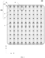
- FIG. 1 is a schematic diagram of a plane structure of a solar cell 200 according to one or more embodiments of the present disclosure.
- An electrode structure 100 includes busbars 1, fingers 2, and electrode pads 3.
- the busbars 1 extend along a first direction X, each of the busbars 1 includes two sub-busbars 4 arranged opposite to each other along a second direction Y, each of the sub-busbars 4 includes first sub-portions 5 and second sub-portions 6 that are spaced from each other, the electrode pads 3 are sandwiched between the first sub-portions 5 of the two sub-busbars 4 and connected to the first sub-portions 5, the first sub-portions 5 of at least one of the sub-busbars 4 protrude towards the side away from the electrode pads 3, and the second direction Y intersects with the first direction X.
- a maximum distance between adjacent first sub-portions 5 in one of the busbars 1 is l 1
- a distance between adjacent second sub-portions 6 in one of the busbars 1 is l 2
- the fingers 2 extend along the second direction Y and are arranged on two sides of the busbar 1 and connected to the sub-busbars 4.
- FIG. 1 merely illustrates that each first sub-portion 5 protrudes towards the side away from the electrode pad 3.
- the first sub-portions 5 of only one sub-busbar 4 protrude towards the side away from the electrode pad 3.
- the first sub-portions 5 of two sub-busbars 4 protruding towards the side away from the electrode pads 3 are alternately arranged. Details are not described herein.
- FIG. 1 illustrates that lengths of the second sub-portions 6 are all equal along the first direction X. In practical applications, a distance between two adjacent first sub-portions 5 of one sub-busbar 4 may be adjusted through the lengths of the second sub-portions 6 along the first direction X.
- numbers of the busbars 1, the fingers 2, and the electrode pads 3 in FIG. 1 are only illustrative, which may be adjusted as required.
- the fingers 2 have the function of collecting carriers and transmitting the carriers to the busbars 1, the busbars 1 conduct the collected currents to the electrode pads 3, and the electrode pads 3 are connected to the solder strip to conduct the current out.
- the busbars 1 and the fingers 2 are integrally manufactured by screen printing, or the busbars 1 and the fingers 2 are printed separately, which is not limited herein.
- the busbars 1 and the fingers 2 are generally made of silver, but are not limited thereto, which may also be made of aluminum or other materials as required.
- the busbars 1 each include two sub-busbars 4, so that the solder strip can be limited between the two sub-busbars 4 of the busbar 1 and the solder strip can directly contact the electrode pads 3, which reduces micro cracks during the soldering of the solder strip with the electrode pads 3 and can reduce the repair rate caused by the micro cracks during the soldering.
- the repair rate is reduced by 39%, and a layer repair rate is reduced from 16.93% to 10.31%.
- the electrode structure 100 according to this embodiment has at least the following beneficial effects.
- the busbars 1 extend along a first direction X, each of the busbars 1 includes two sub-busbars 4 arranged opposite to each other along a second direction Y, and each of the sub-busbars 4 includes first sub-portions 5 and second sub-portions 6 that are spaced from each other.
- the solder strip is limited between the two sub-busbars 4 of one of the busbars 1 and can directly contact the electrode pads 3, which helps to improve soldering tension between the solder strip and the electrode pads 3 and can also reduce the probability of micro cracks during assembly.
- the electrode pads 3 are sandwiched between the first sub-portions 5 of the two sub-busbars 4 and connected to the first sub-portions 5, the first sub-portions 5 of at least one of the sub-busbars 4 protrude towards the side away from the electrode pads 3, and the second direction Y intersects with the first direction X. Since the electrode pads 3 are connected to the first sub-portions 5 and the first sub-portions 5 are expanded, a soldering window is widened. Along a direction perpendicular to a plane where the electrode structure 100 is located, differences exist between heights of the sub-busbars 4 and heights of the electrode pads 3, which may not affect the connection between the solder strip and the electrode pads 3.
- the solder strip may be at least partially connected to the electrode pads 3, which effectively avoids cold soldering during the soldering of the electrode pads 3 with the solder strip.
- the range is appropriately defined as 1.2 ⁇ l 1 /l 2 ⁇ 2.
- l 1 /l 2 is less than 1.2, in one of the busbars 1, a difference between the maximum distance between the adjacent first sub-portions 5 and the distance between the adjacent second sub-portions 6 is small, which is not conducive to the manufacturing and does not evidently avoid the cold soldering.
- l 1 /l 2 is greater than 2, silver paste may be wasted, and a double-side performance of a solar cell using the electrode structure 100 is affected.
- FIG. 2 is a schematic diagram of a plane structure of another solar cell 200 according to one or more embodiments of the present disclosure.
- Connecting end portions 7 are arranged at two ends of the sub-busbars 4, the connecting end portions 7 are connected to the first sub-portions 5.
- widths of the connecting end portions 7 in the second direction Y gradually decrease along a direction from the first sub-portions 5 pointing to the connecting end portions 7.
- connecting end portions 7 are connected to the second sub-portions 6, and in the connecting end portions 7 and the second sub-portions 6 that are connected, widths of the connecting end portions 7 in the second direction Y gradually decrease along a direction from the second sub-portions 6 pointing to the connecting end portions 7.
- FIG. 1 illustrates that two ends of the connecting end portions 7 are connected to the first sub-portions 5, and FIG. 2 illustrates that the two ends of the connecting end portions 7 are connected to the second sub-portions 6.
- the connecting end portions 7 have one end connected to the first sub-portions 5 and the other end connected to the second sub-portions 6. Details are not described herein.
- Orthographic projections of the connecting end portions 7 in the direction of the plane where the electrode structure 100 is located may be trapezoidal or triangular.
- FIG. 1 and FIG. 2 only illustrate that all the electrode pads 3 are rectangles of a same size.
- FIG. 1 and FIG. 2 only illustrate that the solar cell using the electrode structure 100 according to embodiments of the present disclosure is divided into two half-cut cells, which may certainly also be designed as multiple cut cells according to actual requirements and is not limited herein.
- the current may be conducted to either of the two electrode pads 3.
- the sub-busbars 4 between the electrode pads 3 in the head and edges of the electrode structure 100 can only conduct the current to the electrode pads 3 in the head.
- the sub-busbars 4 between the electrode pads 3 in the tail and the edges of the electrode structure 100 can only conduct the current to the electrode pads 3 in the tail.
- widths of the connecting end portions 7 arranged at two ends of the sub-busbars 4 along the second direction Y are designed as gradually varying with a gradient, which can help to collect currents at the edges of the electrode structure 100, improve conductivity efficiency, and alleviate blackening at the edges of the electrode structure 100.
- FIG. 3 is an enlarged view of portion A in FIG. 1 . Distances between the connecting end portions 7 of the two sub-busbars 4 in one of the busbars 1 are equal along the second direction Y.
- a projection of a region between two opposite connecting end portions 7 in the direction of the plane where the electrode structure 100 is located is rectangular.
- a solder strip is arranged in the rectangular region, so that the solder strip can be ensured to be located between the two sub-busbars 4 of one busbar 1, thereby preventing cold soldering caused by height differences between the connecting end portions 7 and the electrode pads 3 due to the connection of the solder strip with the connecting end portions 7.
- the distances between the connecting end portions 7 of the two sub-busbars 4 in one of the busbars 1 range from 0.5 mm to 3.0 mm along the second direction Y.
- the distances between the connecting end portions 7 of the two sub-busbars 4 when the distances between the connecting end portions 7 of the two sub-busbars 4 are less than 0.5 mm, the requirement on the soldering is relatively high. When the distances between the connecting end portions 7 of the two sub-busbars 4 are greater than 3.0 mm, transfer efficiency may be affected. In the present disclosure, the distances between the connecting end portions 7 of the two sub-busbars 4 in one of the busbars 1 ranging from 0.5 mm to 3.0 mm can meet the requirement on the soldering and can also ensure the transfer efficiency.
- the distances between the connecting end portions 7 of the two sub-busbars 4 in one of the busbars 1 along the second direction Y depend on the width of the solder strip along the second direction Y, which may be adjusted based on actual requirements.
- the distances between the connecting end portions 7 of the two sub-busbars 4 in one of the busbars 1 range from 0.5 mm to 3.0 mm along the second direction Y, but is not limited thereto.
- widths of the sides of the connecting end portions 7 away from the electrode pads 3 are greater than or equal to 0.1 mm, and widths of the sides of the connecting end portions 7 close to the electrode pads 3 are less than or equal to 2 mm.
- the connecting end portions 7 are generally formed by paste printing, but in this way, it is difficult to make the widths of the sides of the connecting end portions 7 away from the electrode pads 3 less than 0.1 mm along the second direction Y. If the widths of the sides of the connecting end portions 7 close to the electrode pads 3 are greater than 2 mm along the second direction Y, a double-side performance of the solar cell using the electrode structure 100 may be affected.
- widths of the sides of the connecting end portions 7 away from the electrode pads 3 are greater than or equal to 0.1 mm, and widths of the sides of the connecting end portions 7 close to the electrode pads 3 are less than or equal to 2 mm, which can satisfy printing requirements and can also ensure the double-side performance of the solar cell using the electrode structure 100.
- shapes and sizes of the connecting end portions 7 are designed according to sizes of the busbars 1, which may vary as the widths of the busbars 1 along the second direction Y change.
- the widths of the sides of the connecting end portions 7 away from the electrode pads 3 along the second direction Y are determined, since the widths of the connecting end portions 7 along the second direction Y are designed as gradually varying with a gradient, the widths of the sides of the connecting end portions 7 close to the electrode pads 3 along the second direction Y are greater than the widths of the sides of the connecting end portions 7 away from the electrode pads 3 along the second direction Y.
- widths of the sides of the connecting end portions 7 away from the electrode pads 3 are greater than or equal to 0.1 mm, and widths of the sides of the connecting end portions 7 close to the electrode pads 3 are less than or equal to 2 mm, but is not limited thereto.
- At least 3 electrode pads 3 are provided.
- the number of the electrode pads 3 is generally even, such as 4, 6, or 8, but the specific setting may be adjusted according to an actual requirement.
- a plurality of electrode pads 3 may be provided. If the electrode structure 100 has a plurality of electrode pads 3, current conduction is more uniform, which is conducive to improving the efficiency of the electrode structure 100. At the same time, electroluminescence (EL) of the module is brighter, which is conducive to improving power of the module.
- EL electroluminescence
- the two sub-busbars 4 of one of the busbars 1 are symmetrically arranged.
- the maximum distance l 1 between the adjacent first sub-portions 5 ranges from 1.2 mm to 1.8 mm along the second direction Y.
- the distance l 2 between the adjacent second sub-portions 6 ranges from 0.9 mm to 1.5 mm along the second direction Y.
- the widths of the electrode pads 3 along the second direction Y may be reduced, and the contact area between the electrode pads 3 and the solder strip may be reduced. If the maximum distance l 1 between the adjacent first sub-portions 5 is greater than 1.8 mm along the second direction Y, the widths of the electrode pads 3 along the second direction Y may be increased, resulting in unnecessary waste.
- the distance l 2 between the adjacent second sub-portions 6 is less than the maximum distance l 1 between the adjacent first sub-portions 5.
- the maximum distance l 1 between the adjacent first sub-portions 5 ranges from 1.2 mm to 1.8 mm along the second direction Y and the distance l 2 between the adjacent second sub-portions 6 ranges from 0.9 mm to 1.5 mm along the second direction Y, which facilitates good soldering of the electrode pads 3 with the solder strip.
- the electrode pads 3 are in contact with the sub-busbars 4, and a length of a contact region ranges from 0.5 mm to 5.0 mm.
- the electrode pads 3 is in contact with the sub-busbars 4, and a length of a contact region ranging from 0.5 mm to 5.0 mm can facilitate the soldering and can also save the amount of silver paste and reduce the costs.
- the electrode pads 3 match the first sub-portions 5, and the lengths of the electrode pads 3 along the first direction X are less than or equal to the lengths of the first sub-portions 5 along the first direction X.
- the length of the contact region ranges from 0.5 mm to 5.0 mm along the first direction X, which can ensure effectiveness of the contact. The range is not limited thereto, which may be adjusted as required.
- widths of the sub-busbars 4 range from 0.2 mm to 0.6 mm along the second direction Y.
- widths of the sub-busbars 4 when the widths of the sub-busbars 4 are less than 0.2 mm, efficiency of current conduction is affected.
- widths of the sub-busbars 4 are greater than 0.6 mm, the efficiency of current conduction is improved, but the double-side performance of the solar cell using the electrode structure 100 in this situation may be reduced.
- widths of the sub-busbars 4 ranging from 0.2 mm to 0.6 mm along the second direction Y can satisfy efficiency of current transfer of the sub-busbars 4 and can also ensure the double-side performance of the solar cell using the electrode structure 100 described as above.
- the widths of the busbars 1 along the second direction Y range from 1.0 mm to 1.5 mm. Widths of the busbars 1 according to the present disclosure along the second direction Y range from 0.4 mm to 1.2 mm, so that the widths of the busbars 1 according to the present disclosure along the second direction Y are narrower than those in the related art, which can reduce the amount of silver paste, reduce shielded regions, and increase the double-side performance of the solar cell using the electrode structure 100 in this embodiment.
- widths of the sub-busbars 4 range from 0.2 mm to 0.6 mm along the second direction Y, and the widths of the busbars 1 along the second direction Y may also be set to be wider than or equal to those in the related art according to an actual requirement, which is not limited herein.
- FIG. 4 is a sectional view taken along a direction A-A' in FIG. 3 .
- the solar cell 200 includes: a silicon wafer 8, the silicon wafer 8 is provided with an emitter layer 9 on one side; a first passivation layer 10 arranged on the side of the emitter layer 9 away from the silicon wafer 8; a second passivation layer 11 arranged on the side of the silicon wafer 8 away from the emitter layer 9; and an electrode structure 100 arranged on the side of the first passivation layer 10 away from the silicon wafer 8, and/or arranged on the side of the second passivation layer 11 away from the silicon wafer 8.
- the electrode structure 100 is the electrode structure 100 described above.
- FIG. 4 only illustrates that the solar cell 200 is a Passivated Emitter and Rear Cell (PERC) double-sided cell.
- the electrode structure 100 is arranged on the side of the second passivation layer 11 away from the silicon wafer 8.
- the electrode structure 100 may be arranged only on the side of the first passivation layer 10 away from the silicon wafer 8 or only on the side of the second passivation layer 11 away from the silicon wafer 8, or the electrode structure 100 is arranged on both the side of the first passivation layer 10 away from the silicon wafer 8 and the side of the second passivation layer 11 away from the silicon wafer 8, thereby increasing the double-side performance of the solar cell 200.
- the solar cell 200 may also be an N-type Tunnel Oxide Passivated Contact (TOPCon) solar cell or other types of solar cells.
- the N-type TOPCon solar cell includes a first passivation layer 10, an emitter layer 9, a silicon wafer 8, an ultra-thin oxide layer, a doped polysilicon layer, and a back passivation layer.
- the solar cell 200 according to some embodiments of the present disclosure has the beneficial effects of the electrode structure 100 according to embodiments of the present disclosure. Details can be obtained with reference to the description of the electrode structure 100 in the above embodiments, which are not described herein.
- FIG. 5 is a schematic structural diagram of a photovoltaic module 300 according to one or more embodiments of the present disclosure.
- the photovoltaic module 300 includes a transparent cover plate 12, an upper packaging layer 13, a solar cell 200, a lower packaging layer 14, and a back plate 15.
- the solar cell 200 is the solar cell 200 described above. It may be understood that the photovoltaic module 300 according to the present disclosure has the beneficial effects of the solar cell 200 according to the present disclosure. Details can be obtained with reference to the description of the solar cell 200 in the above embodiments, which are not described herein.
- the electrode structure, the solar cell, and the photovoltaic module according to the present disclosure achieve at least the following beneficial effects.
- the busbars extend along a first direction, each of the busbars includes two sub-busbars arranged opposite to each other along a second direction, and each of the sub-busbars includes first sub-portions and second sub-portions that are spaced from each other.
- the solder strip is limited between the two sub-busbars of one of the busbars and can directly contact the electrode pads, which helps to improve soldering tension between the solder strip and the electrode pads and can also reduce the probability of micro cracks during assembly.
- the electrode pads are sandwiched between the first sub-portions of the two sub-busbars and connected to the first sub-portions, the first sub-portions of at least one of the sub-busbars protrude towards the side away from the electrode pads, and the second direction intersects with the first direction. Since the electrode pads are connected to the first sub-portions and the first sub-portions are expanded, a soldering window is widened. Along the direction perpendicular to the plane where the electrode structure is located, differences exist between heights of the sub-busbars and heights of the electrode pads, which may not affect the connection between the solder strip and the electrode pads.
- the solder strip may be at least partially connected to the electrode pads, which effectively avoids cold soldering during the soldering of the electrode pads with the solder strip.
- the range of l 1 /l 2 is set as 1.2 ⁇ l l /l 2 ⁇ 2, to avoid the situations when l 1 /l 2 is less than 1.2, in one of the busbars, a difference between the maximum distance between the adjacent first sub-portions and the distance between the adjacent second sub-portions is small, which is not conducive to the manufacturing and does not evidently avoid the cold soldering; and when l 1 /l 2 is greater than 2, silver paste may be wasted, and a double-side performance of a solar cell using the electrode structure is affected.
Landscapes
- Photovoltaic Devices (AREA)
- Hybrid Cells (AREA)
Claims (13)
- Structure d'électrode (100), appliquée à une cellule solaire, comprenant :une pluralité de paires (2) de sous-barres omnibus (4) comprenant chacune deux sous-barres omnibus (4) s'étendant le long d'une première direction et agencées à l'opposé l'une de l'autre le long d'une deuxième direction coupant la première direction, dans laquelle, pour chaque paire de sous-barres omnibus (4), chacune des sous-barres omnibus (4) inclut des premières sous-parties (5) et des deuxièmes sous-parties (6), deux premières sous-parties (5) étant chacune agencées sur une sous-barre omnibus respective de la paire de sous-barres omnibus (4) sont espacées à un premier intervalle le long de la deuxième direction, et deux deuxièmes sous-parties (6) étant chacune agencée sous une sous-barre omnibus respective de la paire de sous-barres omnibus (4) sont espacées au niveau d'un deuxième intervalle le long de la deuxième direction ;des doigts (2) s'étendant le long de la deuxième direction sont agencés des deux côtés de chaque paire de sous-barres omnibus (4), dans laquelle les doigts (2) sont connectés aux sous-barres omnibus (4) etdes pastilles d'électrode (3) pour la connexion à un ruban de soudure, les pastilles d'électrode (3) étant intercalées entre les premières sous-parties (5) agencées sur une sous-barre omnibus respective de chaque paire de sous-barres omnibus (4) et connectées aux premières sous-parties (5), dans lequel le premier intervalle entre les premières sous-parties (5) agencées sur une sous-barre omnibus respective d'une paire de sous-barres omnibus (4) est supérieur au deuxième intervalle entre les deuxièmes sous-parties (6) agencées sur une sous-barre omnibus respective de la paire de sous-barres omnibus (4),dans lequel des parties d'extrémité de connexion (7) pour connecter un ruban de soudure sont prévues aux deux extrémités de chacune des sous-barres omnibus (4), les parties d'extrémité de connexion (7) sont connectées aux premières sous-parties (5) et pour les parties d'extrémité de connexion (7) et les premières sous-parties (5) qui sont connectées les unes aux autres, les largeurs des parties d'extrémité de connexion (7) dans la deuxième direction diminuent graduellement le long d'une direction allant des premières sous-parties (5) vers les parties d'extrémité de connexion (7) et/ou les parties d'extrémité de connexion (7) sont connectées aux deuxièmes sous-parties (6) et pour les parties d'extrémité de connexion (7) et les deuxièmes sous-parties (6) qui sont connectées les unes aux autres, les largeurs des parties d'extrémité de connexion (7) dans la deuxième direction diminuent graduellement le long d'une direction allant des deuxièmes sous-parties (6) vers les parties d'extrémité de connexion (7).
- Structure d'électrode (100) selon la revendication 1, dans lequel le long de la deuxième directionun premier intervalle maximal entre les premières sous-parties (5) agencées sur une sous-barre omnibus respective de la paire de sous-barres omnibus (4) est I1,le deuxième intervalle entre les deuxièmes sous-parties (6) agencées sur une sous-barre omnibus respective de la paire de sous-barres omnibus (4) est I2, où 1.2≤I1≤I2≤2.
- Structure d'électrode (100) selon la revendication 1, dans laquelle le long de la deuxième direction, les distances entres les parties d'extrémité de connexion (7) prévues à une extrémité d'une sous-barre omnibus respective de la paire de sous-barres omnibus (4) sont égales.
- Structure d'électrode (100) selon la revendication 3, dans laquelle le long de la deuxième direction, la distance entre les parties d'extrémité de connexion (7) prévues à une extrémité d'une sous-barre omnibus respective de la paire de sous-barres omnibus (4) est comprise entre 0.5 mm et 3.0 mm.
- Structure d'électrode (100) selon la revendication 1, dans laquelle le long de la deuxième direction une largeur d'un côté de la partie d'extrémité de connexion (7) se détournant de la pastille d'électrode (3) est supérieure ou égale à 0.1 mm.
- Structure d'électrode (100) selon la revendication 1, dans laquelle le long de la deuxième direction, une largeur d'un côté de la partie d'extrémité de connexion (7) proche de la pastille d'électrode (3) est inférieure ou égale à 2 mm.
- Structure d'électrode (100) selon la revendication 1, dans laquelle les deux sous-barres omnibus de la paire de sous-barres omnibus (4) sont agencées symétriquement ; et
le long de la deuxième direction, un premier intervalle maximal entre deux premières sous-parties (5) chacune agencées sur une sous-barre omnibus respective de la paire de sous-barres omnibus (4) est compris 1.2 mm et 1.8 mm. - Structure d'électrode (100) selon la revendication 1, dans laquelle les deux sous-barres omnibus de la paire de de sous-barres omnibus (4) sont agencées symétriquement ; et
le long de la deuxième direction, le deuxième intervalle entre deux deuxièmes sous-parties (6) chacune agencée sur une sous-barre omnibus respective de la paire de sous-barres omnibus (4) est compris entre 0.9 mm et 1.5 mm. - Structure d'électrode (100) selon la revendication 1, dans laquelle le long de la première direction, les pastilles d'électrodes (3) sont en contact avec les sous-barres omnibus (4) et une longueur d'une région de contact est comprise entre 0.5 mm et 5.0 mm.
- Structure d'électrode (100) selon la revendication 1, dans laquelle, pour chaque paire de sous-barres omnibus (4), au moins 3 pastilles d'électrodes (3) sont prévues.
- Structure d'électrode (100) selon la revendication 1, dans laquelle le long de la deuxième direction, une largeur de chacune des sous-barres omnibus (4) est comprise entre 0.2 mm et 0.6 mm.
- Cellule solaire (200), comprenant :une plaquette de silicium (8) comprenant une couche émettrice (9) sur un côté de la plaquette de silicium (8) ;une première couche de passivation (10) agencée sur un côté de la couche émettrice (9) se détournant de la plaquette de silicium (8) ;une deuxième couche de passivation (11) agencée sur un côté de la plaquette de silicium (8) se détournant de la couche émettrice (9) ; etune structure d'électrode (100) selon une quelconque des revendications 1 à 11 agencée sur un côté de la première couche de passivation (10) se détournant de la plaquette de silicium (8) et/ou agencée sur un côté de la deuxième couche de passivation (11) se détournant de la plaquette de silicium (8).
- Module photovoltaïque (300), comprenant une plaque de couvercle transparente (12), une couche d'encapsulation supérieure (13), une couche d'encapsulation inférieure (14) et un fond de panier (15) et au moins une cellule solaire (200) selon la revendication 12.
Priority Applications (1)
| Application Number | Priority Date | Filing Date | Title |
|---|---|---|---|
| EP23207592.9A EP4300594A3 (fr) | 2021-10-29 | 2022-10-13 | Structure d'électrode, cellule solaire et module photovoltaïque |
Applications Claiming Priority (1)
| Application Number | Priority Date | Filing Date | Title |
|---|---|---|---|
| CN202122636021.0U CN216015381U (zh) | 2021-10-29 | 2021-10-29 | 电极结构、太阳能电池及光伏组件 |
Related Child Applications (2)
| Application Number | Title | Priority Date | Filing Date |
|---|---|---|---|
| EP23207592.9A Division EP4300594A3 (fr) | 2021-10-29 | 2022-10-13 | Structure d'électrode, cellule solaire et module photovoltaïque |
| EP23207592.9A Division-Into EP4300594A3 (fr) | 2021-10-29 | 2022-10-13 | Structure d'électrode, cellule solaire et module photovoltaïque |
Publications (3)
| Publication Number | Publication Date |
|---|---|
| EP4174959A1 EP4174959A1 (fr) | 2023-05-03 |
| EP4174959C0 EP4174959C0 (fr) | 2024-02-07 |
| EP4174959B1 true EP4174959B1 (fr) | 2024-02-07 |
Family
ID=80526638
Family Applications (2)
| Application Number | Title | Priority Date | Filing Date |
|---|---|---|---|
| EP23207592.9A Pending EP4300594A3 (fr) | 2021-10-29 | 2022-10-13 | Structure d'électrode, cellule solaire et module photovoltaïque |
| EP22201298.1A Active EP4174959B1 (fr) | 2021-10-29 | 2022-10-13 | Structure d'électrode, cellule solaire et module photovoltaïque |
Family Applications Before (1)
| Application Number | Title | Priority Date | Filing Date |
|---|---|---|---|
| EP23207592.9A Pending EP4300594A3 (fr) | 2021-10-29 | 2022-10-13 | Structure d'électrode, cellule solaire et module photovoltaïque |
Country Status (10)
| Country | Link |
|---|---|
| US (3) | US12021157B2 (fr) |
| EP (2) | EP4300594A3 (fr) |
| JP (2) | JP7349545B2 (fr) |
| CN (1) | CN216015381U (fr) |
| AT (1) | AT17955U1 (fr) |
| AU (2) | AU2022252710B2 (fr) |
| DE (1) | DE202022106063U1 (fr) |
| FR (1) | FR3128824B3 (fr) |
| GB (2) | GB2612449B (fr) |
| NL (1) | NL2033414B1 (fr) |
Families Citing this family (5)
| Publication number | Priority date | Publication date | Assignee | Title |
|---|---|---|---|---|
| CN114639749A (zh) * | 2022-05-20 | 2022-06-17 | 英利能源发展有限公司 | 一种光伏组件及其封装方法 |
| CN218215317U (zh) * | 2022-08-03 | 2023-01-03 | 隆基绿能科技股份有限公司 | 一种太阳能电池和太阳能组件 |
| CN117457788B (zh) * | 2023-10-08 | 2025-03-11 | 西安隆基乐叶光伏科技有限公司 | 一种太阳能电池的制作方法、太阳能电池和电池串 |
| CN118431305B (zh) * | 2024-04-16 | 2025-08-19 | 隆基绿能科技股份有限公司 | 一种太阳能电池、光伏组件及其制造方法 |
| DE212024000084U1 (de) * | 2024-04-28 | 2025-04-03 | Longi Green Energy Technology Co., Ltd. | Solarzelle und Photovoltaikmodul |
Family Cites Families (30)
| Publication number | Priority date | Publication date | Assignee | Title |
|---|---|---|---|---|
| JP2000164901A (ja) | 1998-11-27 | 2000-06-16 | Kyocera Corp | 太陽電池 |
| JP2001068699A (ja) | 1999-08-30 | 2001-03-16 | Kyocera Corp | 太陽電池 |
| JP4412842B2 (ja) | 2000-11-27 | 2010-02-10 | 京セラ株式会社 | 太陽電池 |
| JP4578123B2 (ja) | 2004-03-05 | 2010-11-10 | 京セラ株式会社 | 太陽電池モジュール |
| JP5368022B2 (ja) | 2008-07-17 | 2013-12-18 | 信越化学工業株式会社 | 太陽電池 |
| KR20120062431A (ko) * | 2010-12-06 | 2012-06-14 | 엘지전자 주식회사 | 태양전지 |
| JP2013004509A (ja) | 2011-06-10 | 2013-01-07 | Self:Kk | Led灯具 |
| CN102544128B (zh) | 2011-12-28 | 2014-05-21 | 江西赛维Ldk太阳能高科技有限公司 | 一种太阳能电池 |
| TWI502756B (zh) | 2012-11-09 | 2015-10-01 | Big Sun Energy Technology Inc | 具有粗細匯流排電極之太陽能電池 |
| JP6064769B2 (ja) | 2013-04-23 | 2017-01-25 | 三菱電機株式会社 | 太陽電池モジュール及び太陽電池セル |
| CN203760489U (zh) | 2014-02-26 | 2014-08-06 | 中电投西安太阳能电力有限公司 | 电极栅线结构 |
| KR101613364B1 (ko) | 2014-09-05 | 2016-04-18 | 현대중공업 주식회사 | 태양전지의 전면전극 구조 |
| JP2016178280A (ja) | 2014-11-28 | 2016-10-06 | 京セラ株式会社 | 太陽電池素子およびこれを用いた太陽電池モジュール |
| WO2016117180A1 (fr) | 2015-01-21 | 2016-07-28 | 三菱電機株式会社 | Élément de batterie solaire, module de batterie solaire, procédé de fabrication d'un élément de batterie solaire, et procédé de fabrication d'un module de batterie solaire |
| CN106098803B (zh) | 2015-05-22 | 2017-10-17 | 苏州沃特维自动化系统有限公司 | 一种太阳能电池片单元制备方法及太阳能电池组件 |
| DE202015004065U1 (de) * | 2015-06-09 | 2015-07-30 | Solarworld Innovations Gmbh | Solarzellenanordnung |
| KR101751727B1 (ko) | 2015-06-10 | 2017-07-11 | 엘지전자 주식회사 | 태양 전지의 제조 방법 |
| CN105514183B (zh) | 2015-11-30 | 2017-10-17 | 黄河水电光伏产业技术有限公司 | 一种晶硅太阳能电池正面电极的制备方法 |
| CN105552145B (zh) | 2016-01-28 | 2017-08-11 | 黄河水电光伏产业技术有限公司 | 一种晶硅太阳能电池 |
| KR101890291B1 (ko) | 2017-02-03 | 2018-08-22 | 엘지전자 주식회사 | 태양 전지 |
| CN208000923U (zh) | 2018-03-22 | 2018-10-23 | 青海黄河上游水电开发有限责任公司光伏产业技术分公司 | 一种无主栅线的太阳能电池 |
| CN109037367A (zh) | 2018-08-15 | 2018-12-18 | 友达光电股份有限公司 | 一种多主栅太阳能电池 |
| KR102576589B1 (ko) | 2018-09-05 | 2023-09-08 | 상라오 징코 솔라 테크놀러지 디벨롭먼트 컴퍼니, 리미티드 | 태양 전지 및 이를 포함하는 태양 전지 패널 |
| IT201900009072A1 (it) * | 2019-06-14 | 2020-12-14 | Enel Green Power Italia S R L | Cella solare ottimizzata, modulo di celle solari e relativo metodo di produzione. |
| CN211428184U (zh) | 2020-02-21 | 2020-09-04 | 浙江晶科能源有限公司 | 一种太阳能电池板及光伏组件 |
| CN212659550U (zh) | 2020-08-10 | 2021-03-05 | 苏州阿特斯阳光电力科技有限公司 | 光伏组件 |
| CN212303685U (zh) * | 2020-09-08 | 2021-01-05 | 天合光能股份有限公司 | 晶体硅太阳能电池背电极图形结构 |
| CN213459749U (zh) | 2020-10-20 | 2021-06-15 | 江苏隆基乐叶光伏科技有限公司 | 一种电池片和光伏组件 |
| CN213459753U (zh) | 2020-11-24 | 2021-06-15 | 上饶捷泰新能源科技有限公司 | 一种太阳能电池及其栅线结构、光伏组件 |
| CN112635586A (zh) | 2020-12-30 | 2021-04-09 | 通威太阳能(成都)有限公司 | 一种高效高可靠性perc太阳能电池及其正面电极和制作方法 |
-
2021
- 2021-10-29 CN CN202122636021.0U patent/CN216015381U/zh active Active
-
2022
- 2022-10-11 AU AU2022252710A patent/AU2022252710B2/en active Active
- 2022-10-12 US US17/964,502 patent/US12021157B2/en active Active
- 2022-10-13 EP EP23207592.9A patent/EP4300594A3/fr active Pending
- 2022-10-13 JP JP2022164474A patent/JP7349545B2/ja active Active
- 2022-10-13 EP EP22201298.1A patent/EP4174959B1/fr active Active
- 2022-10-27 DE DE202022106063.0U patent/DE202022106063U1/de active Active
- 2022-10-27 AT ATGM70/2022U patent/AT17955U1/de unknown
- 2022-10-27 FR FR2211203A patent/FR3128824B3/fr active Active
- 2022-10-28 GB GB2216013.9A patent/GB2612449B/en active Active
- 2022-10-28 GB GB2314053.6A patent/GB2622146B/en active Active
- 2022-10-28 NL NL2033414A patent/NL2033414B1/en active
-
2023
- 2023-09-11 JP JP2023147129A patent/JP7471500B2/ja active Active
-
2024
- 2024-01-05 AU AU2024200079A patent/AU2024200079B2/en active Active
- 2024-04-02 US US18/624,403 patent/US12328970B2/en active Active
-
2025
- 2025-04-22 US US19/186,112 patent/US20250255037A1/en active Pending
Also Published As
| Publication number | Publication date |
|---|---|
| EP4174959C0 (fr) | 2024-02-07 |
| US20250255037A1 (en) | 2025-08-07 |
| CN216015381U (zh) | 2022-03-11 |
| AU2022252710B2 (en) | 2023-12-21 |
| FR3128824A3 (fr) | 2023-05-05 |
| US20240250190A1 (en) | 2024-07-25 |
| FR3128824B3 (fr) | 2023-11-10 |
| GB202314053D0 (en) | 2023-11-01 |
| JP2023158216A (ja) | 2023-10-26 |
| US12021157B2 (en) | 2024-06-25 |
| EP4300594A2 (fr) | 2024-01-03 |
| EP4174959A1 (fr) | 2023-05-03 |
| AU2022252710A1 (en) | 2023-05-18 |
| GB2612449A (en) | 2023-05-03 |
| JP7471500B2 (ja) | 2024-04-19 |
| DE202022106063U1 (de) | 2022-12-19 |
| GB2612449B (en) | 2023-10-25 |
| GB2622146A (en) | 2024-03-06 |
| JP2023067779A (ja) | 2023-05-16 |
| GB202216013D0 (en) | 2022-12-14 |
| AU2024200079B2 (en) | 2025-08-07 |
| GB2622146B (en) | 2025-02-19 |
| EP4300594A3 (fr) | 2024-04-10 |
| JP7349545B2 (ja) | 2023-09-22 |
| US20230139905A1 (en) | 2023-05-04 |
| NL2033414B1 (en) | 2023-12-21 |
| US12328970B2 (en) | 2025-06-10 |
| NL2033414A (en) | 2023-05-25 |
| AT17955U1 (de) | 2023-08-15 |
| AU2024200079A1 (en) | 2024-01-25 |
Similar Documents
| Publication | Publication Date | Title |
|---|---|---|
| EP4174959B1 (fr) | Structure d'électrode, cellule solaire et module photovoltaïque | |
| EP4220739B1 (fr) | Cellule photovoltaïque et module photovoltaïque | |
| US20230420579A1 (en) | Photovoltaic module | |
| EP4386864B1 (fr) | Cellule solaire et module photovoltaïque | |
| WO2025130437A1 (fr) | Cellule solaire, module photovoltaïque et son procédé de fabrication | |
| EP4727009A1 (fr) | Module photovoltaïque | |
| CN109119497B (zh) | 一种硅基太阳能电池结构 | |
| CN119923031A (zh) | 一种背接触电池以及光伏组件 | |
| US20230253515A1 (en) | Photovoltaic cell and photovoltaic module | |
| CN213184316U (zh) | 异质结太阳能电池及光伏组件 | |
| EP3267492B1 (fr) | Cellule solaire | |
| CN222814783U (zh) | 一种太阳能电池、电池组件及光伏系统 | |
| EP4646065A1 (fr) | Maille d'impression de colle et module photovoltaïque | |
| CN222396019U (zh) | 一种异质结太阳能电池片及异质结太阳能电池 | |
| CN222692207U (zh) | 太阳能电池片及太阳能电池组件 | |
| EP4646066A1 (fr) | Module photovoltaïque et grille d'impression à la colle | |
| CN215815895U (zh) | 电池片和具有其的光伏组件 | |
| AU2025252514A1 (en) | Photovoltaic module | |
| CN115332370A (zh) | 电池片和光伏组件 |
Legal Events
| Date | Code | Title | Description |
|---|---|---|---|
| PUAI | Public reference made under article 153(3) epc to a published international application that has entered the european phase |
Free format text: ORIGINAL CODE: 0009012 |
|
| STAA | Information on the status of an ep patent application or granted ep patent |
Free format text: STATUS: REQUEST FOR EXAMINATION WAS MADE |
|
| 17P | Request for examination filed |
Effective date: 20221013 |
|
| AK | Designated contracting states |
Kind code of ref document: A1 Designated state(s): AL AT BE BG CH CY CZ DE DK EE ES FI FR GB GR HR HU IE IS IT LI LT LU LV MC ME MK MT NL NO PL PT RO RS SE SI SK SM TR |
|
| RIN1 | Information on inventor provided before grant (corrected) |
Inventor name: QIU, YANKAI Inventor name: ZHOU, JING Inventor name: XU, QIANG |
|
| GRAP | Despatch of communication of intention to grant a patent |
Free format text: ORIGINAL CODE: EPIDOSNIGR1 |
|
| STAA | Information on the status of an ep patent application or granted ep patent |
Free format text: STATUS: GRANT OF PATENT IS INTENDED |
|
| INTG | Intention to grant announced |
Effective date: 20231011 |
|
| RIN1 | Information on inventor provided before grant (corrected) |
Inventor name: QIU, YANKAI Inventor name: ZHOU, JING Inventor name: XU, QIANG |
|
| GRAS | Grant fee paid |
Free format text: ORIGINAL CODE: EPIDOSNIGR3 |
|
| GRAA | (expected) grant |
Free format text: ORIGINAL CODE: 0009210 |
|
| STAA | Information on the status of an ep patent application or granted ep patent |
Free format text: STATUS: THE PATENT HAS BEEN GRANTED |
|
| AK | Designated contracting states |
Kind code of ref document: B1 Designated state(s): AL AT BE BG CH CY CZ DE DK EE ES FI FR GB GR HR HU IE IS IT LI LT LU LV MC ME MK MT NL NO PL PT RO RS SE SI SK SM TR |
|
| REG | Reference to a national code |
Ref country code: GB Ref legal event code: FG4D |
|
| REG | Reference to a national code |
Ref country code: CH Ref legal event code: EP |
|
| REG | Reference to a national code |
Ref country code: IE Ref legal event code: FG4D |
|
| REG | Reference to a national code |
Ref country code: DE Ref legal event code: R096 Ref document number: 602022001868 Country of ref document: DE |
|
| U01 | Request for unitary effect filed |
Effective date: 20240301 |
|
| U07 | Unitary effect registered |
Designated state(s): AT BE BG DE DK EE FI FR IT LT LU LV MT NL PT SE SI Effective date: 20240311 |
|
| PG25 | Lapsed in a contracting state [announced via postgrant information from national office to epo] |
Ref country code: IS Free format text: LAPSE BECAUSE OF FAILURE TO SUBMIT A TRANSLATION OF THE DESCRIPTION OR TO PAY THE FEE WITHIN THE PRESCRIBED TIME-LIMIT Effective date: 20240607 |
|
| PG25 | Lapsed in a contracting state [announced via postgrant information from national office to epo] |
Ref country code: GR Free format text: LAPSE BECAUSE OF FAILURE TO SUBMIT A TRANSLATION OF THE DESCRIPTION OR TO PAY THE FEE WITHIN THE PRESCRIBED TIME-LIMIT Effective date: 20240508 |
|
| PG25 | Lapsed in a contracting state [announced via postgrant information from national office to epo] |
Ref country code: RS Free format text: LAPSE BECAUSE OF FAILURE TO SUBMIT A TRANSLATION OF THE DESCRIPTION OR TO PAY THE FEE WITHIN THE PRESCRIBED TIME-LIMIT Effective date: 20240507 Ref country code: HR Free format text: LAPSE BECAUSE OF FAILURE TO SUBMIT A TRANSLATION OF THE DESCRIPTION OR TO PAY THE FEE WITHIN THE PRESCRIBED TIME-LIMIT Effective date: 20240207 |
|
| PG25 | Lapsed in a contracting state [announced via postgrant information from national office to epo] |
Ref country code: ES Free format text: LAPSE BECAUSE OF FAILURE TO SUBMIT A TRANSLATION OF THE DESCRIPTION OR TO PAY THE FEE WITHIN THE PRESCRIBED TIME-LIMIT Effective date: 20240207 |
|
| PG25 | Lapsed in a contracting state [announced via postgrant information from national office to epo] |
Ref country code: RS Free format text: LAPSE BECAUSE OF FAILURE TO SUBMIT A TRANSLATION OF THE DESCRIPTION OR TO PAY THE FEE WITHIN THE PRESCRIBED TIME-LIMIT Effective date: 20240507 Ref country code: NO Free format text: LAPSE BECAUSE OF FAILURE TO SUBMIT A TRANSLATION OF THE DESCRIPTION OR TO PAY THE FEE WITHIN THE PRESCRIBED TIME-LIMIT Effective date: 20240507 Ref country code: IS Free format text: LAPSE BECAUSE OF FAILURE TO SUBMIT A TRANSLATION OF THE DESCRIPTION OR TO PAY THE FEE WITHIN THE PRESCRIBED TIME-LIMIT Effective date: 20240607 Ref country code: HR Free format text: LAPSE BECAUSE OF FAILURE TO SUBMIT A TRANSLATION OF THE DESCRIPTION OR TO PAY THE FEE WITHIN THE PRESCRIBED TIME-LIMIT Effective date: 20240207 Ref country code: GR Free format text: LAPSE BECAUSE OF FAILURE TO SUBMIT A TRANSLATION OF THE DESCRIPTION OR TO PAY THE FEE WITHIN THE PRESCRIBED TIME-LIMIT Effective date: 20240508 Ref country code: ES Free format text: LAPSE BECAUSE OF FAILURE TO SUBMIT A TRANSLATION OF THE DESCRIPTION OR TO PAY THE FEE WITHIN THE PRESCRIBED TIME-LIMIT Effective date: 20240207 |
|
| PG25 | Lapsed in a contracting state [announced via postgrant information from national office to epo] |
Ref country code: PL Free format text: LAPSE BECAUSE OF FAILURE TO SUBMIT A TRANSLATION OF THE DESCRIPTION OR TO PAY THE FEE WITHIN THE PRESCRIBED TIME-LIMIT Effective date: 20240207 |
|
| PG25 | Lapsed in a contracting state [announced via postgrant information from national office to epo] |
Ref country code: PL Free format text: LAPSE BECAUSE OF FAILURE TO SUBMIT A TRANSLATION OF THE DESCRIPTION OR TO PAY THE FEE WITHIN THE PRESCRIBED TIME-LIMIT Effective date: 20240207 |
|
| PG25 | Lapsed in a contracting state [announced via postgrant information from national office to epo] |
Ref country code: SM Free format text: LAPSE BECAUSE OF FAILURE TO SUBMIT A TRANSLATION OF THE DESCRIPTION OR TO PAY THE FEE WITHIN THE PRESCRIBED TIME-LIMIT Effective date: 20240207 |
|
| PG25 | Lapsed in a contracting state [announced via postgrant information from national office to epo] |
Ref country code: CZ Free format text: LAPSE BECAUSE OF FAILURE TO SUBMIT A TRANSLATION OF THE DESCRIPTION OR TO PAY THE FEE WITHIN THE PRESCRIBED TIME-LIMIT Effective date: 20240207 |
|
| PG25 | Lapsed in a contracting state [announced via postgrant information from national office to epo] |
Ref country code: SK Free format text: LAPSE BECAUSE OF FAILURE TO SUBMIT A TRANSLATION OF THE DESCRIPTION OR TO PAY THE FEE WITHIN THE PRESCRIBED TIME-LIMIT Effective date: 20240207 |
|
| PG25 | Lapsed in a contracting state [announced via postgrant information from national office to epo] |
Ref country code: SM Free format text: LAPSE BECAUSE OF FAILURE TO SUBMIT A TRANSLATION OF THE DESCRIPTION OR TO PAY THE FEE WITHIN THE PRESCRIBED TIME-LIMIT Effective date: 20240207 Ref country code: SK Free format text: LAPSE BECAUSE OF FAILURE TO SUBMIT A TRANSLATION OF THE DESCRIPTION OR TO PAY THE FEE WITHIN THE PRESCRIBED TIME-LIMIT Effective date: 20240207 Ref country code: RO Free format text: LAPSE BECAUSE OF FAILURE TO SUBMIT A TRANSLATION OF THE DESCRIPTION OR TO PAY THE FEE WITHIN THE PRESCRIBED TIME-LIMIT Effective date: 20240207 Ref country code: CZ Free format text: LAPSE BECAUSE OF FAILURE TO SUBMIT A TRANSLATION OF THE DESCRIPTION OR TO PAY THE FEE WITHIN THE PRESCRIBED TIME-LIMIT Effective date: 20240207 |
|
| REG | Reference to a national code |
Ref country code: DE Ref legal event code: R097 Ref document number: 602022001868 Country of ref document: DE |
|
| U20 | Renewal fee for the european patent with unitary effect paid |
Year of fee payment: 3 Effective date: 20241025 |
|
| PLBE | No opposition filed within time limit |
Free format text: ORIGINAL CODE: 0009261 |
|
| STAA | Information on the status of an ep patent application or granted ep patent |
Free format text: STATUS: NO OPPOSITION FILED WITHIN TIME LIMIT |
|
| 26N | No opposition filed |
Effective date: 20241108 |
|
| PG25 | Lapsed in a contracting state [announced via postgrant information from national office to epo] |
Ref country code: MC Free format text: LAPSE BECAUSE OF FAILURE TO SUBMIT A TRANSLATION OF THE DESCRIPTION OR TO PAY THE FEE WITHIN THE PRESCRIBED TIME-LIMIT Effective date: 20240207 |
|
| PG25 | Lapsed in a contracting state [announced via postgrant information from national office to epo] |
Ref country code: IE Free format text: LAPSE BECAUSE OF NON-PAYMENT OF DUE FEES Effective date: 20241013 |
|
| U20 | Renewal fee for the european patent with unitary effect paid |
Year of fee payment: 4 Effective date: 20251028 |
|
| PG25 | Lapsed in a contracting state [announced via postgrant information from national office to epo] |
Ref country code: CY Free format text: LAPSE BECAUSE OF FAILURE TO SUBMIT A TRANSLATION OF THE DESCRIPTION OR TO PAY THE FEE WITHIN THE PRESCRIBED TIME-LIMIT; INVALID AB INITIO Effective date: 20221013 |
|
| PG25 | Lapsed in a contracting state [announced via postgrant information from national office to epo] |
Ref country code: HU Free format text: LAPSE BECAUSE OF FAILURE TO SUBMIT A TRANSLATION OF THE DESCRIPTION OR TO PAY THE FEE WITHIN THE PRESCRIBED TIME-LIMIT; INVALID AB INITIO Effective date: 20221013 |