EP4175178A1 - Gate-unit für einen gate-kommutierten thyristor und integrierter gate-kommutierter thyristor - Google Patents
Gate-unit für einen gate-kommutierten thyristor und integrierter gate-kommutierter thyristor Download PDFInfo
- Publication number
- EP4175178A1 EP4175178A1 EP21205354.0A EP21205354A EP4175178A1 EP 4175178 A1 EP4175178 A1 EP 4175178A1 EP 21205354 A EP21205354 A EP 21205354A EP 4175178 A1 EP4175178 A1 EP 4175178A1
- Authority
- EP
- European Patent Office
- Prior art keywords
- gate
- voltage
- unit
- turn
- supply potential
- Prior art date
- Legal status (The legal status is an assumption and is not a legal conclusion. Google has not performed a legal analysis and makes no representation as to the accuracy of the status listed.)
- Withdrawn
Links
- 238000004891 communication Methods 0.000 claims description 15
- 238000000034 method Methods 0.000 claims description 3
- 230000007423 decrease Effects 0.000 description 10
- 208000002454 Nasopharyngeal Carcinoma Diseases 0.000 description 4
- 230000000903 blocking effect Effects 0.000 description 4
- 239000000835 fiber Substances 0.000 description 3
- 238000005259 measurement Methods 0.000 description 3
- 239000004065 semiconductor Substances 0.000 description 3
- 238000013459 approach Methods 0.000 description 2
- 239000003990 capacitor Substances 0.000 description 2
- 230000000295 complement effect Effects 0.000 description 2
- 238000013461 design Methods 0.000 description 2
- 238000005516 engineering process Methods 0.000 description 2
- 230000010354 integration Effects 0.000 description 2
- 239000013307 optical fiber Substances 0.000 description 2
- 230000003071 parasitic effect Effects 0.000 description 2
- 230000000644 propagated effect Effects 0.000 description 2
- 230000001902 propagating effect Effects 0.000 description 2
- 230000008901 benefit Effects 0.000 description 1
- 230000008859 change Effects 0.000 description 1
- 238000006243 chemical reaction Methods 0.000 description 1
- 238000010276 construction Methods 0.000 description 1
- 230000001934 delay Effects 0.000 description 1
- 230000001419 dependent effect Effects 0.000 description 1
- 238000001514 detection method Methods 0.000 description 1
- 238000009828 non-uniform distribution Methods 0.000 description 1
- 230000008092 positive effect Effects 0.000 description 1
- 230000008569 process Effects 0.000 description 1
- 230000009467 reduction Effects 0.000 description 1
- 229920006395 saturated elastomer Polymers 0.000 description 1
- 238000007493 shaping process Methods 0.000 description 1
Images
Classifications
-
- H—ELECTRICITY
- H03—ELECTRONIC CIRCUITRY
- H03K—PULSE TECHNIQUE
- H03K17/00—Electronic switching or gating, i.e. not by contact-making and –breaking
- H03K17/51—Electronic switching or gating, i.e. not by contact-making and –breaking characterised by the components used
- H03K17/80—Electronic switching or gating, i.e. not by contact-making and –breaking characterised by the components used using non-linear magnetic devices; using non-linear dielectric devices
-
- H—ELECTRICITY
- H03—ELECTRONIC CIRCUITRY
- H03K—PULSE TECHNIQUE
- H03K17/00—Electronic switching or gating, i.e. not by contact-making and –breaking
- H03K17/13—Modifications for switching at zero crossing
- H03K17/136—Modifications for switching at zero crossing in thyristor switches
-
- H—ELECTRICITY
- H02—GENERATION; CONVERSION OR DISTRIBUTION OF ELECTRIC POWER
- H02M—APPARATUS FOR CONVERSION BETWEEN AC AND AC, BETWEEN AC AND DC, OR BETWEEN DC AND DC, AND FOR USE WITH MAINS OR SIMILAR POWER SUPPLY SYSTEMS; CONVERSION OF DC OR AC INPUT POWER INTO SURGE OUTPUT POWER; CONTROL OR REGULATION THEREOF
- H02M1/00—Details of apparatus for conversion
- H02M1/0048—Circuits or arrangements for reducing losses
- H02M1/0054—Transistor switching losses
- H02M1/0058—Transistor switching losses by employing soft switching techniques, i.e. commutation of transistors when applied voltage is zero or when current flow is zero
-
- H—ELECTRICITY
- H02—GENERATION; CONVERSION OR DISTRIBUTION OF ELECTRIC POWER
- H02M—APPARATUS FOR CONVERSION BETWEEN AC AND AC, BETWEEN AC AND DC, OR BETWEEN DC AND DC, AND FOR USE WITH MAINS OR SIMILAR POWER SUPPLY SYSTEMS; CONVERSION OF DC OR AC INPUT POWER INTO SURGE OUTPUT POWER; CONTROL OR REGULATION THEREOF
- H02M1/00—Details of apparatus for conversion
- H02M1/08—Circuits specially adapted for the generation of control voltages for semiconductor devices incorporated in static converters
-
- H—ELECTRICITY
- H02—GENERATION; CONVERSION OR DISTRIBUTION OF ELECTRIC POWER
- H02M—APPARATUS FOR CONVERSION BETWEEN AC AND AC, BETWEEN AC AND DC, OR BETWEEN DC AND DC, AND FOR USE WITH MAINS OR SIMILAR POWER SUPPLY SYSTEMS; CONVERSION OF DC OR AC INPUT POWER INTO SURGE OUTPUT POWER; CONTROL OR REGULATION THEREOF
- H02M3/00—Conversion of DC power input into DC power output
- H02M3/01—Resonant DC/DC converters
-
- H—ELECTRICITY
- H02—GENERATION; CONVERSION OR DISTRIBUTION OF ELECTRIC POWER
- H02M—APPARATUS FOR CONVERSION BETWEEN AC AND AC, BETWEEN AC AND DC, OR BETWEEN DC AND DC, AND FOR USE WITH MAINS OR SIMILAR POWER SUPPLY SYSTEMS; CONVERSION OF DC OR AC INPUT POWER INTO SURGE OUTPUT POWER; CONTROL OR REGULATION THEREOF
- H02M3/00—Conversion of DC power input into DC power output
- H02M3/22—Conversion of DC power input into DC power output with intermediate conversion into AC
- H02M3/24—Conversion of DC power input into DC power output with intermediate conversion into AC by static converters
- H02M3/28—Conversion of DC power input into DC power output with intermediate conversion into AC by static converters using discharge tubes with control electrode or semiconductor devices with control electrode to produce the intermediate AC
- H02M3/305—Conversion of DC power input into DC power output with intermediate conversion into AC by static converters using discharge tubes with control electrode or semiconductor devices with control electrode to produce the intermediate AC using devices of a thyratron or thyristor type requiring extinguishing means
- H02M3/315—Conversion of DC power input into DC power output with intermediate conversion into AC by static converters using discharge tubes with control electrode or semiconductor devices with control electrode to produce the intermediate AC using devices of a thyratron or thyristor type requiring extinguishing means using semiconductor devices only
- H02M3/3155—Conversion of DC power input into DC power output with intermediate conversion into AC by static converters using discharge tubes with control electrode or semiconductor devices with control electrode to produce the intermediate AC using devices of a thyratron or thyristor type requiring extinguishing means using semiconductor devices only with automatic control of the output voltage or current
-
- H—ELECTRICITY
- H03—ELECTRONIC CIRCUITRY
- H03K—PULSE TECHNIQUE
- H03K17/00—Electronic switching or gating, i.e. not by contact-making and –breaking
- H03K17/04—Modifications for accelerating switching
- H03K17/0403—Modifications for accelerating switching in thyristor switches
-
- H—ELECTRICITY
- H03—ELECTRONIC CIRCUITRY
- H03K—PULSE TECHNIQUE
- H03K17/00—Electronic switching or gating, i.e. not by contact-making and –breaking
- H03K17/04—Modifications for accelerating switching
- H03K17/041—Modifications for accelerating switching without feedback from the output circuit to the control circuit
- H03K17/0412—Modifications for accelerating switching without feedback from the output circuit to the control circuit by measures taken in the control circuit
-
- H—ELECTRICITY
- H03—ELECTRONIC CIRCUITRY
- H03K—PULSE TECHNIQUE
- H03K2217/00—Indexing scheme related to electronic switching or gating, i.e. not by contact-making or -breaking covered by H03K17/00
- H03K2217/0036—Means reducing energy consumption
-
- Y—GENERAL TAGGING OF NEW TECHNOLOGICAL DEVELOPMENTS; GENERAL TAGGING OF CROSS-SECTIONAL TECHNOLOGIES SPANNING OVER SEVERAL SECTIONS OF THE IPC; TECHNICAL SUBJECTS COVERED BY FORMER USPC CROSS-REFERENCE ART COLLECTIONS [XRACs] AND DIGESTS
- Y02—TECHNOLOGIES OR APPLICATIONS FOR MITIGATION OR ADAPTATION AGAINST CLIMATE CHANGE
- Y02B—CLIMATE CHANGE MITIGATION TECHNOLOGIES RELATED TO BUILDINGS, e.g. HOUSING, HOUSE APPLIANCES OR RELATED END-USER APPLICATIONS
- Y02B70/00—Technologies for an efficient end-user side electric power management and consumption
- Y02B70/10—Technologies improving the efficiency by using switched-mode power supplies [SMPS], i.e. efficient power electronics conversion e.g. power factor correction or reduction of losses in power supplies or efficient standby modes
Definitions
- the present invention relates to soft-switching power electronics devices which utilize IGCTs as a semiconductor switch. Particularly, the present invention relates to gate units for gate commutated thyristors that are particularly suited for soft-switching applications.
- Integrated-gate commutated thyristors are thyristor-based semiconductor switching devices that integrate a gate commutated thyristor (GCT) and a gate unit for controlling the switching of the GCT in a single switching module.
- GCT gate commutated thyristor
- IGCTs In high-power medium-voltage applications, IGCTs have proven to achieve remarkable efficiencies and high-power density. Furthermore, these power switches proved to be robust and reliable, and come with typically very high voltage and current ratings, making them suitable for MW level power conversion. Typically, these devices have very low conduction losses, being another reason for their use in high power applications. However, IGCTs have high switching losses which effectively limits their efficiency and the applicable switching frequencies. Typically, IGCT devices are switched with frequencies below 1kHz in industrial converters, which are in most cases AC-DC hard-switched rectifiers or inverters. Consequently, state of the art gate units are designed for hard-switched low frequency operation.
- Soft-switching implies additional measures and can be generally realized as zero-current switching (ZCS) or zero-voltage switching (ZVS).
- ZCS zero-current switching
- ZVS zero-voltage switching
- the device's current anode-cathode-current
- the device's blocking voltage anode-cathode-voltage
- GCT gate-commutated thyristor
- a gate unit for controlling a gate commutated thyristor comprising:
- the gate unit and the IGCT will be used in applications where they can be operated in a zero-current switching or zero-voltage switching operation mode.
- IGCTs can be applied in applications, such as an LLC resonant converter with a zero-voltage switching during turn-on or a series resonant converter with a zero-current switching during turn-on.
- gate units for IGCTs are generally designed to implement the following functions which are conventionally implemented in separate hardware stages:
- the gate control unit may be configured to operate switching of the gate commutated thyristor in soft-switching mode, particularly in a zero voltage switching mode or a zero current switching mode.
- the gate unit is relatively complex, which affects its size that poses practical restrictions on the mechanical construction of the IGCT stack and increases the overall cost.
- the IGCT is either nonconducting after the turn on (in ZVS operation), or the current builds up very slowly after the turn on (in ZCS operation).
- the current rate of rise (current slope) is also limited when the retrigger pulse is required.
- both the turn-on pulse and the retrigger pulse can be reduced in magnitude. This reduction in peak current ratings reduces power flow during switching and, therefore, directly reduces the cost of these power stages.
- a turn-off stage may be provided configured to apply the negative supply potential to selectively turn off the GCT.
- the central idea of the invention is to integrate the turn-on function, the retrigger function, the positive-gate-voltage backporch function, and the negative-gate-voltage backporch function into a single power stage. This is possible because in the applications with ZVS or ZCS turn on, the current slope di/dt of the anode current after turning on (or retrigger pulse generation) is very low. Hence, the thyristor cells within the GCT have significantly more time to open uniformly without causing hot-spotting problems (a nonuniform distribution of current in the wafer, potentially leading to a GCT failure). As a consequence, the turn-on and retrigger pulses can be reduced in magnitude. This opens the possibility for the simplification of the gate unit.
- the power stage may comprise a transistor-switched voltage selector, such as a T-type NPC stage, e.g. formed by four MOSFETs, whose output is coupled with a single nonlinear saturable inductor.
- the power stage may be controlled by a gate control unit and may be operated to accomplish functions of the conventional turn-on stage, the retrigger stage, the positive-gate-voltage backporch stage and the negative-gate-voltage backporch stage. capable of connecting a high supply voltage potential, a middle supply voltage potential and a low supply voltage potential in a controlled manner.
- the output of the transistor-switched voltage selector is coupled via the nonlinear inductor with a gate terminal of the GCT.
- the transistor-switched voltage selector can be used to have complete control over the turn-on states by adjusting the voltage drop over the nonlinear inductor.
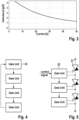
- the inductor is configured as a nonlinear inductor which may actively be driven into saturation or operated in saturation. At low currents the inductor is not yet saturated and provides an inductance for backporch operation modes which is sufficiently high so that the current ripple is reasonably low while maintaining reasonably low switching frequencies. During high currents, the inductor should saturate and, therefore, decrease its inductance to enable higher current slopes di/dt of the turn-on and retrigger pulses.
- This nonlinear characteristic also decreases the energy which can be stored in the inductor during the turn-on and the retrigger pulse generation. Therefore, the inductor size can be made smaller and the pulse loading of the high-supply voltage bus is lower.
- the use of a single nonlinear saturable inductor simplifies the topology of the gate unit significantly.
- the power stage is capable to support the combined operation modes, such as turn-on, positive voltage backporch operation, negative gate voltage backporch operation and retrigger operation as follows:
- the nonlinearity of the nonlinear inductor is selected so that the low inductance for the turn-on pulse generation has a value at least 50% lower than the high inductance during the backporch operation. While the high inductance value might be a clear requirement to achieve ripple sufficiently low, the low value of inductance can be selected slightly more freely.
- the gate unit comprises a communication channel output to interlink with a control input of another gate unit wherein the gate control unit is configured to propagate a control signal received via the control input through the communication channel output, wherein the control signal includes switching commands for the gate commutated thyristors.
- the gate unit may comprise a communication channel output to interlink with a control input of another gate unit wherein the gate control unit is configured to propagate an control signal received via the control input through the communication channel output, wherein the control signal includes an error signal indicating the occurrence of an error in one of the gate units wherein the gate control unit is further configured to halt operation of the gate unit once an error signal has been received.
- an integrated gate commutated thyristor comprising a gate commutated thyristor and the above gate unit is provided.
- a converter stage for use in a converter system comprising a number of integrated gate commutated thyristors each including a gate commutated thyristor and the above gate unit, wherein one of the gate units is coupled with a central controller to receive the control signal and at least a part of the other gate units are respectively coupled via its communication channel output with the control input of a further one of the other gate units, so that the control signal is available in all gate units.
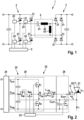
- FIG. 1 schematically shows circuitry for an LLC resonant converter 1 with an active inverter stage 2, a resonant tank 4, and a rectifier stage 3.
- the inverter stage 2 comprises a bridge circuit of four gate-commutated thyristors 21 (GCT), each controlled by an individual gate unit 22 for operating or controlling the switching the GCT 21.
- GCT gate-commutated thyristors 21
- the gate units 22 are controlled by a central controller 5 for converter operation by commanding switching on or switching off of each of the GCTs. Switching on and off of the GCTs 21 is handled by the corresponding gate units 22.
- the inverter stage 2 is made of two separate inverter series connections of GCTs 21 which are coupled with the resonant tank 4 via their middle nodes.
- the resonant tank 4 comprises a series connection of a first capacitor 41 and a first inductance 42 at a first of the middle nodes wherein a second inductance 43 connects the series connection with a second of the middle nodes of the inverter stage 2.
- the resonant tank 4 is coupled with the rectifier 3, e.g. implemented as a passive diode rectifier with diodes 31.
- the central controller 5 is capable of operating the LLC resonant converter 1 in a zero-voltage switching or zero-current switching mode to improve the efficiency of converter 1.
- converter 1 is configured to be operated in the zero-voltage switching mode or zero-current switching mode, as in these operation modes, the value of the current slope di/dt of the anode current after turn-on pulse is relatively low.
- appropriate voltage and/or current measurement units for measuring cathode-anode voltage /current are implemented in the IGCT formed by the respective GCT 21 and gate unit 22.
- FIG. 2 schematically shows the circuitry of one of the gate units 22 in more detail.
- Each gate unit 22 has a similar or identical configuration.
- the gate unit 22 uses a power supply 24 which generally provides three supply voltage potential levels, such as a high supply potential V pos , a middle supply potential V mid and a negative supply potential V neg .
- the power supply 24 of the gate unit may be powered by an (not shown) external medium-voltage-isolating power supply.
- a power stage 25 is connected with the power supply 24 basically comprises a voltage selector 26 comprising switching transistors, such as MOSFETs, to connect one of the supply potentials V pos , V mid , V neg to a selector output node N.
- the selector output node N is coupled with a nonlinear inductor 27 to the gate unit output G to be applied to a respective gate terminal of the GCT 21.
- a first switching transistor S T is coupled between the high supply potential V pos and the selector output node N, the middle supply potential V mid is coupled via two switching transistors S M1 , S M2 with the selector output node N, and the low supply potential V neg is coupled via a fourth switching transistor S B with the selector output node N.
- the selector output node N is coupled via the nonlinear inductance 27 with the gate unit output G.
- measurement units for measuring the gate-to-cathode voltage polarity e.g. by comparators
- the inductor current have to be provided.
- the first and second switching transistors S T , S M1 are operated complementary and the third and fourth switching transistors S M2 , S B are operated complementary.
- Control of the switching transistors S T , S M1 , S M2 , S B is made by a gate control unit 23.
- the voltage selector 26 of the power stage has a three-level T-type NPC topology and is configured to provide three voltage levels at the selector output node N.
- a turn-off stage 28 configured to turn off the GCT 21 and to keep it off by applying the negative supply potential V neg between its gate terminal and its cathode terminal. This is made with a turn-off transistor S off also controlled by the gate control unit 23. So, the turn-off stage 28 has the task to connect the gate terminal of the GCT 21 with the low supply potential V neg to discard the charge from the gate terminal in order to turn off the GCT 21.
- the inductor current i on is completely commutated into gate unit 22 for the GCT 21 to restore its blocking capability. Therefore, the low supply potential V neg is buffered by a sufficiently high capacitance C off .
- the control method applied by the gate control unit 23 is as follows:
- the voltage selector 26 of the power stage has a three-level T-type NPC topology and is configured to provide three voltage levels at the selector output node N, thereby avoiding an operation state where a low gate voltage v g of the backporch operation has to be formed by a close to 50-percent duty cycle operation which would in turn require a relatively high switching frequency to keep the gate current i g ripple low.
- the gate control unit 23 controls the operation of the GCT 21 basically based on a comparator value of the gate voltage v g and the measurement of the power stage 25 current e.g. based on a shunt and a current sense amplifier.
- the low supply voltage is applied to ensure that the gate current decreases after the initial pulse as this can be understood as a sign that the antiparallel diode of the gate-commutated thyristor is conducting.
- the backporch operation state is activated depending on the polarity of the gate voltage v g .
- the nonlinear inductor 27 has a nonlinearity to have an inductance sufficiently high during the backporch operation to ensure that an acceptable low current ripple can be achieved at a switching frequency appropriately low and that the inductance is sufficiently low to ensure a fast ramp-up of the gate current i g to generate and propagate the high slope current at turn-on pulse generation and retrigger pulse generation.
- the nonlinear saturable inductor is used that decreases its inductance with increasing currents.
- the nonlinearity is selected so that the low inductance for the turn-on pulse generation has a value at least 50 % lower than the high inductance during the backporch operation.
- gate units 22 may be provided with an interlock function, which may be implemented as an independent function in each of the gate units 22.
- the idea is to provide an additional communication channel 29, such as fiber optics, on the gate units 22 that allows for interlocking the gate units in the case of an error detection in one of the gate units 22.
- the idea is to make an unidirectional ring structure capable of propagating the error state through the gate units 22 without involvement of the central controller 5.
- central controller 5 does not require to possess many fiber optic inputs to get an error state from every single gate unit 22 to disable the application. Moreover, the length of the utilized optical fiber could be shorter, considering that the fiber optic interconnections are only within the IGCT stack.
- an interlink between the series-connected IGCTs 21, 22 is provided to simplify the cabling of optical fibers within the application.
- This approach is configured by an additional communication channel output on each gate unit 22 to enable an option for an interlink.
- gate units 22 propagate the control signal which controls the switching of the IGCTs and only one connection to the central controller 5 is necessary. This significantly simplifies the cabling of the communication channels and also requires lower number of communication outputs at the central controller 5.
- each device Since the turn-on and turn-off need to happen in all IGCTs at the same time, it is recommended to wait for a certain amount of time in each device to compensate for the propagation delays due to communication transmitters and receivers (e.g. 30 ns in first device, 20 ns in second and 10 ns in third, assuming the propagation delay of 10 ns per gate unit).
- the particular waiting time for each IGCT can either be configured manually or it can be programmed to happen automatically during converter power up. This could be implemented by propagating the number via the interlink chain, which would be increased in each gate unit. This would provide sufficient information on how much time has to be waited in the particular IGCT.
Landscapes
- Engineering & Computer Science (AREA)
- Power Engineering (AREA)
- Physics & Mathematics (AREA)
- Nonlinear Science (AREA)
- Power Conversion In General (AREA)
Priority Applications (4)
| Application Number | Priority Date | Filing Date | Title |
|---|---|---|---|
| EP21205354.0A EP4175178A1 (de) | 2021-10-28 | 2021-10-28 | Gate-unit für einen gate-kommutierten thyristor und integrierter gate-kommutierter thyristor |
| PCT/EP2022/079995 WO2023073051A1 (en) | 2021-10-28 | 2022-10-26 | Gate unit for a gate-commutated thyristor and integrated gate-commutated thyristor |
| EP22808822.5A EP4423912B1 (de) | 2021-10-28 | 2022-10-26 | Gate-unit für einen gate-kommutierten thyristor und integrierter gate-kommutierter thyristor |
| US18/702,062 US20250070773A1 (en) | 2021-10-28 | 2022-10-26 | Gate unit for a gate-commutated thyristor and integrated gate-commutated thyristor |
Applications Claiming Priority (1)
| Application Number | Priority Date | Filing Date | Title |
|---|---|---|---|
| EP21205354.0A EP4175178A1 (de) | 2021-10-28 | 2021-10-28 | Gate-unit für einen gate-kommutierten thyristor und integrierter gate-kommutierter thyristor |
Publications (1)
| Publication Number | Publication Date |
|---|---|
| EP4175178A1 true EP4175178A1 (de) | 2023-05-03 |
Family
ID=78414411
Family Applications (2)
| Application Number | Title | Priority Date | Filing Date |
|---|---|---|---|
| EP21205354.0A Withdrawn EP4175178A1 (de) | 2021-10-28 | 2021-10-28 | Gate-unit für einen gate-kommutierten thyristor und integrierter gate-kommutierter thyristor |
| EP22808822.5A Active EP4423912B1 (de) | 2021-10-28 | 2022-10-26 | Gate-unit für einen gate-kommutierten thyristor und integrierter gate-kommutierter thyristor |
Family Applications After (1)
| Application Number | Title | Priority Date | Filing Date |
|---|---|---|---|
| EP22808822.5A Active EP4423912B1 (de) | 2021-10-28 | 2022-10-26 | Gate-unit für einen gate-kommutierten thyristor und integrierter gate-kommutierter thyristor |
Country Status (3)
| Country | Link |
|---|---|
| US (1) | US20250070773A1 (de) |
| EP (2) | EP4175178A1 (de) |
| WO (1) | WO2023073051A1 (de) |
Cited By (1)
| Publication number | Priority date | Publication date | Assignee | Title |
|---|---|---|---|---|
| CN116593938A (zh) * | 2023-07-13 | 2023-08-15 | 湖南大学 | 一种全桥llc谐振变换器开关管开路故障检测方法与电路 |
Families Citing this family (2)
| Publication number | Priority date | Publication date | Assignee | Title |
|---|---|---|---|---|
| CN116260320B (zh) * | 2023-05-12 | 2023-09-05 | 梵塔半导体技术(杭州)有限公司 | 开关电路控制方法、开关电路控制芯片及开关电路 |
| CN120110367A (zh) * | 2025-04-25 | 2025-06-06 | 清华大学 | 关断电路、驱动电路、igct、电气设备和关断方法 |
Citations (2)
| Publication number | Priority date | Publication date | Assignee | Title |
|---|---|---|---|---|
| EP0416933A2 (de) * | 1989-09-08 | 1991-03-13 | Toyo Denki Seizo Kabushiki Kaisha | Treiberschaltung für ein Schaltelement mit grosser Eingangskapazität |
| EP1235334A2 (de) * | 2001-02-27 | 2002-08-28 | Mitsubishi Denki Kabushiki Kaisha | Gate-Treiber für Thyristor |
-
2021
- 2021-10-28 EP EP21205354.0A patent/EP4175178A1/de not_active Withdrawn
-
2022
- 2022-10-26 WO PCT/EP2022/079995 patent/WO2023073051A1/en not_active Ceased
- 2022-10-26 US US18/702,062 patent/US20250070773A1/en active Pending
- 2022-10-26 EP EP22808822.5A patent/EP4423912B1/de active Active
Patent Citations (2)
| Publication number | Priority date | Publication date | Assignee | Title |
|---|---|---|---|---|
| EP0416933A2 (de) * | 1989-09-08 | 1991-03-13 | Toyo Denki Seizo Kabushiki Kaisha | Treiberschaltung für ein Schaltelement mit grosser Eingangskapazität |
| EP1235334A2 (de) * | 2001-02-27 | 2002-08-28 | Mitsubishi Denki Kabushiki Kaisha | Gate-Treiber für Thyristor |
Non-Patent Citations (3)
| Title |
|---|
| H. GRUENING ET AL.: "Proceedings of the 13th International Symposium on Power Semiconductor Devices & ICs. IPSD", 2001, IEEE, article "6 kV 5 kA RCGCT with advanced gate drive unit", pages: 133 - 136 |
| L. XIE ET AL.: "The design of IGCT Gate-Unit equipped in the three-level NPC converter", 2011 INTERNATIONAL CONFERENCE ON ELECTRICAL MACHINES AND SYSTEMS, 2011, pages 1 - 6, XP032020292, DOI: 10.1109/ICEMS.2011.6073530 |
| STIELAU O H ET AL: "A high performance gate/base drive using a current source", CONFERENCE RECORD OF THE INDUSTRY APPLICATIONS SOCIETY ANNUAL MEETING. SEATTLE, OCT. 7 - 12, 1990; [CONFERENCE RECORD OF THE INDUSTRY APPLICATIONS SOCIETY ANNUAL MEETING], NEW YORK, IEEE, US, 7 October 1990 (1990-10-07), pages 1637, XP032134194, ISBN: 978-0-87942-553-1, DOI: 10.1109/IAS.1990.152406 * |
Cited By (2)
| Publication number | Priority date | Publication date | Assignee | Title |
|---|---|---|---|---|
| CN116593938A (zh) * | 2023-07-13 | 2023-08-15 | 湖南大学 | 一种全桥llc谐振变换器开关管开路故障检测方法与电路 |
| CN116593938B (zh) * | 2023-07-13 | 2023-09-26 | 湖南大学 | 一种全桥llc谐振变换器开关管开路故障检测方法与电路 |
Also Published As
| Publication number | Publication date |
|---|---|
| WO2023073051A1 (en) | 2023-05-04 |
| EP4423912B1 (de) | 2026-04-22 |
| US20250070773A1 (en) | 2025-02-27 |
| EP4423912A1 (de) | 2024-09-04 |
Similar Documents
| Publication | Publication Date | Title |
|---|---|---|
| EP4423912B1 (de) | Gate-unit für einen gate-kommutierten thyristor und integrierter gate-kommutierter thyristor | |
| US4639849A (en) | Snubber circuit for H.F. bridge converter | |
| US5351179A (en) | Lossless active snubber for half-bridge output rectifiers | |
| US11671019B2 (en) | Bridge circuit with series-connected switches and control method thereof | |
| US10608522B2 (en) | Electrical circuit with auxiliary voltage source for zero-voltage switching in DC-DC converter under all load conditions | |
| KR100404953B1 (ko) | 컨버터회로장치 | |
| EP3925064B1 (de) | Aufwärtswandler und steuerungsverfahren | |
| EP3633843B1 (de) | Stromwandler und ansteuerverfahren dafür | |
| WO2020003348A1 (ja) | 自己給電回路および電力変換装置 | |
| EP0982827A1 (de) | Kompensatoranordnung und eine Kompensatoranordnung benutzendes Energieübertragungssystem | |
| Lim et al. | Active snubber energy recovery circuit for series-connected IGBTs | |
| EP0588635B1 (de) | Speisespannungsschaltung für Gatesteuerstufe | |
| US5731967A (en) | Converter circuit arrangement with minimal snubber | |
| SK141797A3 (en) | Method for processing pwm waves and devices therefor | |
| CN115459618A (zh) | 一种开关串联的桥式电路及dc/ac变换电路的空载控制方法 | |
| US11146168B2 (en) | Snubber circuit and power conversion apparatus | |
| US20200321874A1 (en) | Power conversion apparatus, and power supply apparatus | |
| JP7021623B2 (ja) | マルチレベル電力変換装置 | |
| Roesner et al. | Cellular driver/snubber scheme for series connection of IGCTs | |
| Zhang et al. | SPETO: A superior power switch for high power, high frequency, low cost converters | |
| WO2024124538A1 (en) | Ac-to-ac power converter | |
| JP2588234B2 (ja) | スナバ回路 | |
| US20260039225A1 (en) | Current sharing of parallel-connected converters | |
| US12489375B2 (en) | Power conversion apparatus including upper and lower arm circuits and a flying capacitor | |
| KR100790748B1 (ko) | 전류원 인버터 |
Legal Events
| Date | Code | Title | Description |
|---|---|---|---|
| PUAI | Public reference made under article 153(3) epc to a published international application that has entered the european phase |
Free format text: ORIGINAL CODE: 0009012 |
|
| STAA | Information on the status of an ep patent application or granted ep patent |
Free format text: STATUS: THE APPLICATION HAS BEEN PUBLISHED |
|
| AK | Designated contracting states |
Kind code of ref document: A1 Designated state(s): AL AT BE BG CH CY CZ DE DK EE ES FI FR GB GR HR HU IE IS IT LI LT LU LV MC MK MT NL NO PL PT RO RS SE SI SK SM TR |
|
| STAA | Information on the status of an ep patent application or granted ep patent |
Free format text: STATUS: THE APPLICATION IS DEEMED TO BE WITHDRAWN |
|
| 18D | Application deemed to be withdrawn |
Effective date: 20231104 |