EP4175312A1 - Capteur d'image - Google Patents
Capteur d'image Download PDFInfo
- Publication number
- EP4175312A1 EP4175312A1 EP22200623.1A EP22200623A EP4175312A1 EP 4175312 A1 EP4175312 A1 EP 4175312A1 EP 22200623 A EP22200623 A EP 22200623A EP 4175312 A1 EP4175312 A1 EP 4175312A1
- Authority
- EP
- European Patent Office
- Prior art keywords
- column
- amplifier
- image sensor
- voltage
- readout
- Prior art date
- Legal status (The legal status is an assumption and is not a legal conclusion. Google has not performed a legal analysis and makes no representation as to the accuracy of the status listed.)
- Granted
Links
Images

Classifications
-
- H—ELECTRICITY
- H04—ELECTRIC COMMUNICATION TECHNIQUE
- H04N—PICTORIAL COMMUNICATION, e.g. TELEVISION
- H04N25/00—Circuitry of solid-state image sensors [SSIS]; Control thereof
- H04N25/70—SSIS architectures; Circuits associated therewith
- H04N25/76—Addressed sensors, e.g. MOS or CMOS sensors
- H04N25/78—Readout circuits for addressed sensors, e.g. output amplifiers or A/D converters
-
- H—ELECTRICITY
- H04—ELECTRIC COMMUNICATION TECHNIQUE
- H04N—PICTORIAL COMMUNICATION, e.g. TELEVISION
- H04N25/00—Circuitry of solid-state image sensors [SSIS]; Control thereof
- H04N25/70—SSIS architectures; Circuits associated therewith
- H04N25/76—Addressed sensors, e.g. MOS or CMOS sensors
- H04N25/767—Horizontal readout lines, multiplexers or registers
-
- H—ELECTRICITY
- H04—ELECTRIC COMMUNICATION TECHNIQUE
- H04N—PICTORIAL COMMUNICATION, e.g. TELEVISION
- H04N25/00—Circuitry of solid-state image sensors [SSIS]; Control thereof
- H04N25/60—Noise processing, e.g. detecting, correcting, reducing or removing noise
- H04N25/65—Noise processing, e.g. detecting, correcting, reducing or removing noise applied to reset noise, e.g. KTC noise related to CMOS structures by techniques other than CDS
-
- H—ELECTRICITY
- H04—ELECTRIC COMMUNICATION TECHNIQUE
- H04N—PICTORIAL COMMUNICATION, e.g. TELEVISION
- H04N25/00—Circuitry of solid-state image sensors [SSIS]; Control thereof
- H04N25/70—SSIS architectures; Circuits associated therewith
- H04N25/76—Addressed sensors, e.g. MOS or CMOS sensors
- H04N25/77—Pixel circuitry, e.g. memories, A/D converters, pixel amplifiers, shared circuits or shared components
-
- H—ELECTRICITY
- H04—ELECTRIC COMMUNICATION TECHNIQUE
- H04N—PICTORIAL COMMUNICATION, e.g. TELEVISION
- H04N25/00—Circuitry of solid-state image sensors [SSIS]; Control thereof
- H04N25/70—SSIS architectures; Circuits associated therewith
- H04N25/76—Addressed sensors, e.g. MOS or CMOS sensors
- H04N25/77—Pixel circuitry, e.g. memories, A/D converters, pixel amplifiers, shared circuits or shared components
- H04N25/772—Pixel circuitry, e.g. memories, A/D converters, pixel amplifiers, shared circuits or shared components comprising A/D, V/T, V/F, I/T or I/F converters
-
- H—ELECTRICITY
- H04—ELECTRIC COMMUNICATION TECHNIQUE
- H04N—PICTORIAL COMMUNICATION, e.g. TELEVISION
- H04N25/00—Circuitry of solid-state image sensors [SSIS]; Control thereof
- H04N25/70—SSIS architectures; Circuits associated therewith
- H04N25/76—Addressed sensors, e.g. MOS or CMOS sensors
- H04N25/77—Pixel circuitry, e.g. memories, A/D converters, pixel amplifiers, shared circuits or shared components
- H04N25/778—Pixel circuitry, e.g. memories, A/D converters, pixel amplifiers, shared circuits or shared components comprising amplifiers shared between a plurality of pixels, i.e. at least one part of the amplifier must be on the sensor array itself
Definitions
- the invention relates to an image sensor for electronic cameras, in particular a CMOS image sensor, having a large number of pixels for generating exposure-dependent signals.
- Electronic cameras are used, for example, as moving image cameras in order to record moving image sequences that are later shown in cinemas. It is important that these cameras have a high image quality. In particular, the brightness, contrast and color of the recorded images are changed during post-processing, and the end product - the processed moving image sequence or the film - is projected onto a large screen in the cinema.
- Each pixel comprises at least: a photosensitive element to generate electric charge from incident light; also a readout node; a transfer gate for selectively coupling the photosensitive element to the readout node and transferring generated charge from the photosensitive element to the readout node; a converter transistor to convert the charge present at the readout node into a voltage signal at a signal output; and a selection switch connected to the signal output of the converter transistor via an output line to select the signal output of the converter transistor selectively coupled to an associated readout line of the image sensor, commonly referred to as a column line.
- CFA color filter array
- Each pixel may also include a reset switch to selectively couple the readout node to a reset potential.
- Such an image sensor can also include a control circuit for generating control signals for the respective transfer gate, the respective selection switch and possibly the respective reset switch of the pixels in order to selectively read out image signals (or image signals and reference signals) from the readout node.
- the converter transistor can form an impedance converter, which generates a voltage signal at its signal output depending on the amount of charge present at its input.
- the column lines of the image sensor can be connected to a respective readout amplifier (commonly referred to as a column amplifier) in order to selectively couple the signal output of the converter transistor to a column line of the image sensor which is associated with a plurality of pixels of the image sensor.
- a number of column lines of the image sensor can also be connected to a signal bus which leads to one or more column amplifier(s) in order to amplify the (possibly already preamplified) voltage signals of a number of column lines.
- the pixels of the image sensor are addressed line by line, for example, and the pixel signals are sent to the column amplifiers (for example at the edge of the pixel array) and from there to an output, where they are digitized and optionally offset against calibration data.
- the image sensors of electronic cameras In order to be able to record moving image sequences even in poor light conditions and to keep the costs for artificial lighting measures on a film set low, it is desirable for the image sensors of electronic cameras to have high light sensitivity.
- the present invention is based on the following considerations.
- the light sensitivity is essentially determined by the noise of the image sensor.
- the lowest signal range is particularly critical in poor lighting conditions.
- the noise of the image sensor essentially consists of the noise of the respective pixel and the noise of the readout path.
- the noise of the readout path can be reduced to values of e.g. 80 ⁇ V (microvolts) by suitable design, so that it only plays a subordinate role compared to the noise of the pixel of e.g. 180 ⁇ V.
- the noise voltage in the respective pixel is largely determined by the converter transistor (e.g. source follower, SF).
- the noise of the pixel is the ratio between the signal voltage that an electron causes and the noise voltage of the converter transistor (SF).
- the noise voltage of the converter transistor must be reduced, or the signal voltage caused by an electron (so-called transconductance) must be increased.
- the light-sensitive element eg pinned diode
- the transfer gate of the pixel By momentarily driving the transfer gate of the pixel, this electron is transferred to the readout node (eg Floating Diffusion, FD) (with a readout process typically transferring a large number of photoelectrically generated electrons).
- the charge of this respective electron acts on the capacitance of the read node (FD) and causes a voltage change there that is inversely proportional to the capacitance of the read node.
- FD Floating Diffusion
- the readout node of the respective pixel can have a capacitance of, for example, 1.6 fF (femtofarads), as a result of which a voltage change of approximately 100 ⁇ V per electron is achieved.
- Other methods such as the use of a guarding structure, can be used to reduce the FD capacitance to 0.6 fF, for example, which means that a voltage change of around 260 ⁇ V per electron can be achieved.
- the capacitance of the readout node is essentially a parasitic capacitance to ground. In order for such capacitances to become ineffective or as small as possible, the voltage at the readout node must remain constant. However, when electrons are transferred from the photosensitive element to the readout node and thereby cause a voltage change at the readout node, this voltage change in turn affects the capacitance of the readout node.
- the voltage at the readout node must be kept constant so that a low capacitance at the readout node and thus a higher signal voltage per electron is achieved and also maintained during a charge transfer to the readout node.
- the column line is associated with a column amplifier, the column line being coupled or capable of being coupled (for example via a switch) to a negative input of the column amplifier via an input capacitor.
- the column amplifier has an amplifier output for outputting an amplifier output signal, the amplifier output having a column readout circuit and is connected to an equalizing line.
- the compensating line can also be referred to as a compensation line.
- the equalizing line is coupled via a respective feedback capacitor to the respective readout node of those pixels which are associated with the column line.
- a negative feedback loop is formed, which includes the column line, the input capacitor, the column amplifier (via its negative input), the equalizing line and the feedback capacitor.
- the feedback capacitor that is (indirectly) coupled or can be coupled to the readout node ensures that the voltage of the readout node can be regulated by the column amplifier or the amplifier output during a charge transfer from the light-sensitive element to the readout node of the respective pixel.
- the voltage at the readout node can be regulated in such a way that there is a reduced capacitance at the readout node. An increased signal voltage per electron can thus be achieved at the readout node of the respective pixel.
- the feedback capacitor thus determines the signal voltage per electron and thus the sensitivity of the pixel.
- a desired signal voltage per electron can be achieved through the feedback and a corresponding dimensioning of the feedback capacitor.
- a readout node capacity of approx. 40 aF (attofarads) is required.
- the feedback capacitor can be dimensioned very small, since the capacitance between the column line and the read-out node is primarily decisive.
- Such an active limitation of the capacity of the readout node is particularly suitable for low signal strengths in poor light conditions, ie for a small number of electrons that are transferred from the light-sensitive element to the readout node per actuation of the transfer gate.
- the light-sensitive element of the respective pixel can also be read out successively in several repetitions, with partial results being achieved which can be added together.
- conventional readout methods can be used without the explained feedback via the feedback capacitor.
- the invention can also be used with a pixel architecture and/or readout architecture that is/are more complex than those mentioned above.
- an overflow capacitor with an additional transfer gate can be provided within the respective pixel, as will be explained below.
- the respective pixel can also have a plurality of light-sensitive elements which are connected or can be coupled via a respective transfer gate to a common readout node (FD) (so-called “sharing") and/or which (alternating in time) have a common converter transistor assigned.
- FD common readout node
- the image sensor it is possible for the image sensor to have a plurality of column lines for each column of pixels, it being possible for a plurality of column lines to be coupled or capable of being coupled to a common column amplifier via a signal bus.
- the electrical voltage is defined as the difference between a first potential (e.g. a generated or considered potential) and a second potential (e.g. a reference potential). is. Insofar as the respective reference potential is given, the two terms can ultimately have the same meaning or be used with the same meaning.
- lines in the image sensor this is to be understood as meaning electrically conductive connections which can be formed in particular on or within a substrate, for example by metallization or doping.
- the column amplifier can be designed to generate the amplifier output signal as a function of the voltage signal of the converter transistor of the respective pixel received via the column line at the input capacitor and to output the amplifier output signal to the column readout circuit and via the equalizing line to the feedback capacitor.
- an electrical voltage generated at the readout node can be output as a voltage signal onto the column line via the converter transistor when the selection switch is open.
- the voltage signal on the column line can follow (in particular as a directly proportional value) the voltage that has been generated at the readout node of the respective pixel, for example due to a charge transfer via the transfer gate.
- the voltage difference between the column line and the negative input of the column amplifier can ensure that the between the Column line and the negative amplifier input arranged input capacitor charges according to the voltage difference.
- the amplifier output signal can assume a different value, as will be explained below.
- the amplifier output signal is transmitted both to the column readout circuit and to the feedback capacitor via the equalizing line.
- the column readout circuit can output corresponding signal values which ultimately correspond to image information.
- the explained feedback loop to the respective readout node can be formed via the compensation line and the feedback capacitor.
- the column readout circuit may be configured to read out the amplifier output signal.
- the column readout circuit can be designed to output a signal value corresponding to the amplifier output signal.
- the column read-out circuit can be designed to read out a reference signal and an image signal as amplifier output signals and to calculate them with one another (in particular by subtraction) in order to eliminate offset values (so-called correlated double sampling), as will be explained below.
- the respective pixel's converter transistor, column line, input capacitor, column amplifier, balance line, and feedback capacitor may form a negative feedback loop for the respective pixel's read node.
- Such a negative feedback loop can counteract an undesired increase in the voltage and thus an undesired increase in the capacitance of the readout node as a result of a charge transfer.
- the input capacitor, the column amplifier and the feedback capacitor of the respective pixel can be designed (arranged and dimensioned) to keep a voltage at the readout node of the respective pixel substantially constant.
- the column amplifier can also form only temporary feedback via the elements mentioned. For the period of feedback, the column amplifier can regulate the voltage on the equalizing line in such a way that the voltage on the readout node of the respective pixel remains essentially constant even in the event of a charge transfer (from the light-sensitive element, via the transfer gate).
- the input capacitor, the column amplifier and the feedback capacitor of the respective pixel can be configured to increase a voltage on the equalization line in the event of a charge increase at the readout node of the respective pixel and thereby essentially compensate for a voltage change at the readout node.
- the fact that the voltage on the column line follows the voltage on the readout node and the voltage on the column line is also available on the column amplifier via the input capacitor can be used for the feedback.
- the column amplifier can include—in addition to the negative amplifier input—a positive amplifier input to which a reference voltage is applied.
- the reference voltage can be used as a reference value in order to carry out the feedback explained and to improve an accuracy of the measurement.
- the reference voltage can be applied to the negative amplifier input be mirrored in order to bring this and the input capacitor connected to it to defined starting values for a subsequent measurement.
- the column amplifier can comprise an operational amplifier with a negative amplifier input and a positive amplifier input.
- the negative amplifier input of the column amplifier can be connected to the amplifier output via a negative feedback line and a negative feedback switch, it being possible for the column amplifier to be brought into negative feedback operation by closing the negative feedback switch, in which there is a potential difference between the voltage on the column line and the input capacitor the reference voltage is set.
- the column amplifier in the negative feedback mode the column amplifier can operate as a voltage follower, i.e. the amplifier output signal can correspond to the input voltage at the positive input of the column amplifier, i.e. the applied reference voltage.
- the column amplifier By subsequently opening the negative feedback switch, the column amplifier, starting from the negative feedback mode, can be brought into an amplification mode in which the amplifier output signal represents a potential difference at the input capacitor that has changed compared to the negative feedback mode.
- the change in the potential difference at the input capacitor can result in particular from an interim charge transfer from the light-sensitive element to the readout node of the respective pixel and a corresponding change in the voltage signal of the respective converter transistor. Consequently, in the amplification mode of the column amplifier, the amplifier output signal can represent a voltage change at the readout node of the respective pixel and thus the number of electrons transferred to the readout node.
- the column amplifier In the amplification mode, the column amplifier can operate in particular as a differential amplifier.
- the image sensor can have a control circuit which is designed to first bring the column amplifier into negative feedback operation for reading out the respective pixel; subsequently bring the column amplifier into the boost mode; thereafter momentarily at least partially opening the transfer gate of the respective pixel to transfer charge into the readout node of the respective pixel; and then to control the column readout circuit for reading out the amplifier output signal, which then represents a signal value or image signal value of the respective pixel.
- the control circuit can, for example, comprise an integrated circuit, a microprocessor or an FPGA.
- the selection switch of the respective pixel can be closed during the entire read-out process of this type.
- the negative feedback operation can be initiated by closing the negative feedback switch.
- the input capacitor can be brought to a defined starting value by means of negative feedback operation.
- the subsequent amplification operation can be initiated by opening the negative feedback switch.
- the amplifier output signal may represent the charge transferred to the readout node of the respective pixel.
- the column amplifier can be in a feedback mode during the amplification mode, i.e. the amplifier output signal is capacitively fed back via the equalizing line and the feedback capacitor to the readout node of the respective pixel.
- each pixel may further include a reset switch to selectively couple the readout node to a reset potential.
- the control circuit may be configured to momentarily close the reset switch of the respective pixel to erase the charge present in the readout node of the respective pixel; and then, in the amplification mode of the column amplifier and before driving (ie opening) the transfer gate, driving the column readout circuit for reading out the amplifier output signal, which then represents a reference value or reference signal value of the respective pixel.
- a magnitude of the voltage change generated by the charge transfer to the readout node can be determined with greater accuracy on the basis of the reference value read out.
- the reference value can be subtracted from the signal value mentioned (determined when the transfer gate is open) (so-called correlated double sampling).
- the column readout circuit can have a reference value readout path and a signal value readout path for this purpose.
- the reference value can be read out via the reference value readout path and the signal value can be read out via the signal value readout path, it being possible for the reference value to be read out and the signal value to be read out at different points in time.
- each pixel may further include an overflow capacitor and another transfer gate to selectively couple the readout node to the overflow capacitor.
- the capacity of the pixel can optionally be temporarily increased in order to be able to absorb large amounts of charge from the light-sensitive element in the event of strong exposure.
- Said control circuit can be designed to also generate control signals for the further transfer gate.
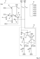
- an exemplary four-transistor APS-type (active pixel sensor) image sensor is described below with reference to FIG 1 explained, with individual components of this image sensor also being present in an image sensor according to the invention.
- the present invention is not limited to active four-transistor image sensors, but can also be used in image sensors with fewer or more than four transistors per pixel, as will be explained below.
- a single pixel 10 is shown as a representative, which includes a light-sensitive element 20 in the form of a photodiode, in particular a so-called pinned diode.
- the light-sensitive element 20 can optionally be charge-coupled via a switch in the form of a transfer gate 21 to a readout node 22, which can be designed in particular as a so-called floating diffusion (FD).
- FD floating diffusion
- the readout node 22 is connected to the gate terminal of a converter transistor 24 designed as a source follower, which is replaced by a field effect transistor (FET) is formed and represents a charge-to-voltage converter circuit. Furthermore, the readout node 22 is connected to a connection 27 of a (for example positive) voltage supply VDD via a further switching device in the form of a reset switch 26 .
- One of the two channel connections (drain connection) of the converter transistor 24 is also connected to the positive voltage supply VDD, whereas the other of the two channel connections (source connection) of the converter transistor 24 forms a signal output 29 at which a voltage signal is output and which is connected to a selection switch 25.
- the selection switch 25 functions as a row selection switch, with the signal output 29 of the converter transistor 24 being able to be selectively coupled to a column line 41 associated with the pixel 10 shown by activating or closing the selection switch 25 .
- the column line 41 (COL) is provided for connecting a plurality or all of the same type pixels 10 arranged in an associated column to a common column amplifier circuit 60 which is arranged, for example, outside the pixel array of the image sensor. This is done alternately by temporarily closing the respective selection switch 25 of the pixel 10.
- the column amplifier circuit 60 includes an input capacitor 61 (CIN) connected to the column line 41 and a voltage node 63 . Furthermore, the column amplifier circuit 60 comprises a column amplifier 65, the negative input 67 of which is connected to the voltage node 63 and the positive input 68 of which a reference voltage VREF is applied. An amplifier capacitor 64 is also connected to an output 69 of the amplifier and the voltage node 63 . In parallel with this, a negative feedback switch 66 is connected to the amplifier output 69 and the voltage node 63 via a negative feedback line.
- the amplifier output 69 is also connected to a column readout circuit 70, which comprises a reference value capacitor 74 of a reference value readout path, the reference value capacitor 74 is connected to ground with one connection and can be selectively coupled to the amplifier output 69 with the other connection via a reference value switch 73 .
- Column readout circuit 70 also includes a signal value capacitor 72 of a signal value readout path, one connection of signal value capacitor 72 also being connected to ground and the other connection also being able to be selectively coupled to amplifier output 69 via a signal value switch 71.
- a pre-charging circuit which includes a current source 62 , is also assigned to the column line 41 outside the pixel field of the image sensor.
- the transfer gate 21 of the respective pixel 10 is via a control line TG1
- the reset switch 26 is via a control line RES
- the selection switch 25 is via a control line SEL
- the negative feedback switch 66 is via a control line FB
- the reference value switch 73 is via a control line SHR
- the signal value switch 71 can be controlled via a control line SHS by a common control circuit 40 of the image sensor.
- CDS Correlated Double Sampling
- the incident light during an exposure process is converted into electric charge by the photosensitive element 20 of each pixel 10, so that the photosensitive element 20 is filled with electrons.
- the control lines TG1, SEL and RES become respectively kept at 0 V, ie the switches 21, 24, 26 controlled thereby are open.
- a voltage of 3.3 V is briefly applied to the control line RES in order to remove charge formed by leakage currents and/or scattered light from the readout node 22, i.e. to erase the readout node 22.
- the readout node 22 is thus set to an initial state defined by the voltage supply VDD.
- a voltage which corresponds to the charge at the cleared readout node 22 is therefore set at the signal output 29 of the converter transistor 24 .
- a voltage of 3.3 V is applied to the control line FB in order to close the negative feedback switch 66 so that the column amplifier 65 is negatively coupled.
- a voltage of VREF is set at the negative input 67 of the column amplifier 65 and thus at the voltage node 63 and at the associated connection of the input capacitor 61 .
- a voltage of 3.3 V is applied to the control line SEL, so that the selection switch 25 is closed.
- a voltage signal from the converter transistor 24 corresponding to the charge in the readout node 22 is switched via the selection switch 25 to the column line 41 and thus to the input capacitor 61 .
- the input capacitor 61 is thus charged to the potential difference between the reference voltage VREF and the voltage on the column line 41.
- the negative feedback switch 66 is opened (control line FB is set to 0 V). The switching process produces a small amount of interference (eg charge injection).
- the column amplifier 65 readjusts accordingly.
- a voltage of 3.3 V is now briefly applied to the control line SHR in order to close the reference value switch 73 and thereby charge the reference value capacitor 74 in accordance with the amplifier output signal. After a renewed opening of the reference value switch 73 a reference value can thus be read from the reference value capacitor 74 .
- a voltage of 3.3 V or less is then briefly applied to the control line TG1 in order to briefly at least partially open the transfer gate 21 of the respective pixel 10 or to close the switch formed thereby, so that the exposure-dependent generated Electrons are transferred from the photosensitive element 20 to the readout node 22 .
- a changed voltage signal of the converter transistor 24 corresponding to the changed charge in the readout node 22 is transmitted to the column line 41 and thus to the input capacitor 61 via the selection switch 25 (again or still closed).
- the column amplifier 65 amplifies this modified signal in relation to the capacitances of the input capacitor 61 and the amplifier capacitor 64 (negative feedback switch 66 remains open) and generates a corresponding modified amplifier output signal at the amplifier output 69 .
- a voltage is now present at the output 69 of the column amplifier 65 which, starting from the initial state of the readout node 22 (offset value), corresponds to the voltage change (voltage drop) due to the transfer of electrical charge from the light-sensitive element 20 to the readout node 22.
- a voltage of 3.3 V is briefly applied to the control line SHS in order to close the signal value switch 71 and thereby charge the signal value capacitor 72 in accordance with the changed amplifier output signal. After the signal value switch 71 is opened again, a signal value (image signal value) can thus be read from the signal value capacitor 72 .
- the difference between the reference value read out and the signal value corresponds to the amount of charge that was transferred from the light-sensitive element 20 to the readout node 22 by opening the transfer gate 21 .
- a voltage of 3.3 V can then be briefly applied to the control line RES again, if necessary, in order to remove the existing charge from the readout node 22 and to repeat the readout process explained for a further partial charge amount, which is achieved by opening the transfer even more -gate 21 is transferred from the photosensitive element 20 to the readout node 22 (readout of a reference value and a signal value).
- a voltage of 3.3 V can be briefly applied to the control lines RES and TG1 in order to remove both the charge from the readout node 22 and any residual charge from the light-sensitive element 20, so that the next exposure process starts with a completely "empty " Pixel 10 can begin.
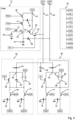
- FIG 2 12 shows parts of an image sensor according to the invention, a four-transistor image sensor being illustrated again by way of example and only a single pixel 10 being shown as a representative, although the image sensor has a multiplicity of pixels 10 arranged in rows and columns.
- the image sensor has a multiplicity of pixels 10 arranged in rows and columns.
- a difference according to the image sensor 1 is that the respective pixel 10 is coupled in addition to the column line 41 to a compensating line 42 (CMP) which runs parallel to the column line 41 and, like the column line 41, is associated with a column of pixels 11.
- the equalizing line 42 is connected to the amplifier output 69 of the column amplifier 65 of the associated column line 41 at one end.
- the compensation line 42 branches to the pixels 11 and 11 associated with the column line 41 is capacitively coupled to the readout node 22 of the respective pixel 10 via a respective feedback capacitor 28 .
- Another difference according to the image sensor 1 is that no amplifier capacitor 64 is arranged between the negative input 67 of the column amplifier 65 and the amplifier output 69, only the negative feedback switch 66.
- the image sensor according to 2 can be operated with high light sensitivity even with small amounts of charge that are transferred from the light-sensitive element 20 to the readout node 22 of the respective pixel 10 and thus enables the recording of moving image sequences even in poor light conditions. This is achieved by a high sensitivity (slope of the amplification characteristic) of the respective readout node 22 .
- the converter transistor 24 of the respective pixel 10, the column line 41, the input capacitor 61, the column amplifier 65, the equalizing line 42 and the feedback capacitor 28 of the respective pixel 10 form a respective negative feedback loop for the read node 22 of the respective pixel 10.
- the negative feedback loop has the effect that a voltage change in the readout node 22, which is caused by the charge carriers transferred from the light-sensitive element 20 to the readout node 22, is compensated for by active feedback of the amplifier output 69 to the readout node 22.
- the column amplifier 65 can counteract a voltage drop at the readout node 22 by increasing the voltage at the amplifier output 69 or on the compensation line 42, so that the voltage at the readout node 22 can be kept essentially constant due to the capacitive coupling via the feedback capacitor 28.
- Parasitic capacitances at readout node 22 thus become essentially ineffective. Therefore, the gain characteristic deteriorates not by the charge carriers transferred to the readout node 22 and an increase in the (parasitic) capacitance caused thereby.
- the feedback capacitor 28 By dimensioning the feedback capacitor 28 with a capacitance of, for example, 40 aF or less, a signal voltage of approximately 4000 ⁇ V per electron can be achieved in the readout node 22, which corresponds to a noise value of 0.05 electrons.
- a MIM (Metal-Insulator-Metal) capacitor can be used as the feedback capacitor 28 by using the capacitance between two line ends.
- a negative feedback operation of the column amplifier 65 can first take place in order to set the input capacitor 61 to a defined starting value, and then an amplification operation of the column amplifier 65 can take place.
- the column amplifier 65 can generate the amplifier output signal as a function of the voltage signal of the converter transistor 24 received at the input capacitor 61 via the column line 41 and output it to the feedback capacitor 28 via the equalizing line 42 .
- a voltage of 3.3 V is briefly applied to the control line RES in order to briefly close the reset switch 26 and erase the readout node 22 (initial state of the readout node 22).
- a voltage is thus set at the signal output 29 of the converter transistor 24 which corresponds to the (residual) charge at the cleared readout node 22 .
- a voltage of 3.3 V is applied to the control line FB in order to close the negative feedback switch 66, so that the column amplifier 65 is negatively coupled. This creates a tension of VREF at the negative input 67 of the column amplifier 65 and thus also at the voltage node 63 and at the associated terminal of the input capacitor 61.
- a voltage of 3.3 V is applied to the control line SEL, so that the selection switch 25 is closed.
- a voltage signal from converter transistor 24 corresponding to the charge in readout node 22 or the output state of readout node 22 is switched via selection switch 25 to column line 41 and thus to input capacitor 61 .
- the input capacitor 61 is thus charged to the potential difference between the reference voltage VREF of the column amplifier 65 and the voltage on the column line 41.
- the negative feedback switch 66 is opened.
- the switching process generates a small amount of interference (e.g. charge injection).
- the column amplifier 65 readjusts according to the voltage difference present at the two inputs 67, 68.
- a voltage of 3.3 V is applied to the control line SHR in order to close the reference value switch 73 and thereby charge the reference value capacitor 74 in accordance with the amplifier output signal.
- a reference value can thus be read from the reference value capacitor 74 .
- a voltage of 3.3 V or less is then applied to the control line TG1 for a short time in order to partially or completely open the transfer gate 21 of the respective pixel 10 for a short time, so that the electrons generated depending on the exposure (or a part thereof) are transferred from the photosensitive element 20 to the readout node 22.
- the selection switch 25 for the connection to the column line 41 can be opened briefly, or the selection switch 25 can be closed remain.
- a changed voltage signal of the converter transistor 24 corresponding to the changed charge in the readout node 22 is transmitted via the selection switch 25 to the column line 41 and thus to the input capacitor 61 .
- the column amplifier 65 Due to the coupling of the input capacitor 61 to the negative input 67 of the column amplifier 65, there is a potential change at the negative input 67.
- the column amplifier 65 generates a modified amplifier output signal at the amplifier output 69, which corresponds to the potential difference between the two inputs 67, 68, i.e. the further potential change relative to VREF.
- the amplifier output signal thus represents the electrical charge which, starting from the initial state of the readout node 22 (offset value), was transferred from the light-sensitive element 20 to the readout node 22 by opening the transfer gate 21 .
- the column amplifier 65 compensates for the effect of the charge on the readout node 22 of the respective pixel 10 by increasing the voltage on the equalization line 42 in accordance with the amplifier output signal until (due to the capacitive coupling with the readout node 22) the voltage on the readout node 22 returns to the original value is equivalent to.
- a voltage of 3.3 V is applied to the control line SHS to momentarily close the signal level switch 71 and thereby charge the signal level capacitor 72 in accordance with the amplifier output signal. After the signal value switch 71 is opened again, a signal value (image signal value) can thus be read from the signal value capacitor 72 . Furthermore, the difference between the reference value read out and the signal value read out can be formed.
- the amplifier output signal is also used for the negative feedback discussed.
- the amplifier output signal is also on via the compensating line 42 the feedback capacitor 28 of the respective pixel 10 to keep the voltage at the sense node 22 substantially constant.
- This readout process can be carried out at least for small amounts of charge or with low exposure.
- the read-out process can also be repeated several times in order to transfer and read out partial amounts of charge to the read-out node 22 by repeatedly opening the transfer gate 21 increasingly.
- the readout method can be combined with other readout methods that allow a larger number of electrons to be read out simultaneously.
- a readout process can take place before or after the readout process explained, during which the negative feedback switch 66 remains closed.
- the VREF voltage is then continuously present on the equalize line 42, and the pixel 10 behaves as an ordinary four-transistor pixel.
- an alternative amplifier circuit 80 may also be used, as discussed below in connection with FIG 3 is explained.
- FIG. 3 illustrates, on the one hand, that parallel to the explained amplifier circuit with feedback via a compensating line 42 (in 3 identified by the reference numeral 60) a further amplifier circuit 80 can also be provided for large amounts of charge (elements of the same type as in the amplifier circuit 60 are identified in the amplifier circuit 80 with reference numerals increased by the number 20).
- different amplification factors can be provided for different amounts of charge in the light-sensitive element 20, for example a lower amplification factor in the amplifier circuit 80 than in the amplifier circuit 60.
- Such a selectable double amplification factor can also be used with a four-transistor pixel 10 according to 2 be provided.
- a further amplifier circuit 80 with a different amplification factor can be provided (so-called “triple gain”).
- the feedback capacitor 28 according to FIG 2 can also be provided, for example, with a five-transistor image sensor.
- the respective pixel 10 according to 3 additionally includes an overflow capacitor 30 and a further transfer gate 31.
- the further transfer gate 31 can be selectively controlled by the control circuit 40 via a control line TG2 to couple the readout node 22 to the overflow capacitor 30.
- the capacitance of the readout node 22 can optionally be temporarily increased in order to be able to absorb large amounts of charge generated in the light-sensitive element 20 when the pixel 10 is exposed to high levels.
- the (temporary) increase in the capacity of the readout node 22 associated with this does not have a disadvantageous effect on the photosensitivity, since a high signal-to-noise ratio is achieved anyway with high exposure.
- the amplifier circuit 80 can be used, which of the connection with 1 explained amplifier circuit corresponds.
- several amplifier circuits 80 of the same type can also be provided in parallel with one another, which, however, have different amplification factors (eg with amplifier capacitors 84 of different sizes), as explained above.
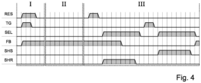
- FIG. 12 illustrates a circuit diagram for a control circuit 40 of an image sensor according to FIG 2 . Shown is the temporal switching sequence for a reset switch 26 (RES), a transfer gate 21 (TG), a selection switch 25 (SEL), a negative feedback switch 66 (FB), a signal value switch 71 (SHS) and a reference value switch 73 (SHR).
- RES reset switch 26
- TG transfer gate 21
- SEL selection switch 25
- FB negative feedback switch 66
- SHS signal value switch 71
- SHR reference value switch 73
- the reset switch 26 (RES) is briefly closed and the transfer gate 21 (TG) is briefly opened in order to empty the photosensitive element 20, i.e. the there to remove existing load carriers.
- the negative feedback switch 66 (FB) is closed. Pixel 10 can now be exposed (time segment II).
- the readout process of the pixel 10 is initiated by briefly closing the reset switch 26 (RES) in order to remove charge formed by leakage currents and/or scattered light from the readout node 22.
- RES reset switch 26
- the selection switch 25 (SEL) and the reference value switch 73 (SHR) are then closed, so that a voltage signal from the converter transistor 24 corresponding to the (residual) charge at the readout node 22 reaches the input capacitor 61 via the column line 41 .
- the negative feedback switch 66 (FB) closed on the column amplifier 65 initially ensures that the column amplifier 65 operates in negative feedback mode and the reference voltage VREF is present at the negative voltage input 67 of the column amplifier 65 .
- the potential difference between the column line 41 and the negative input of the column amplifier 65 results in the input capacitor 61 being charged accordingly.
- the negative feedback switch 66 (FB) is now opened, so that the column amplifier 65 goes into an amplification mode.
- the amplifier output signal now present is at the equalizing line 42.
- the reference value capacitor 74 can be charged according to the amplifier output signal or the voltage at the amplifier output 69 via the closed reference value switch 73 (SHR). Thereafter, the reference value switch 73 (SHR) and the selection switch 25 (SEL) are opened. The reference value capacitor 74 can be read out now or later.
- the signal voltage value is then read out.
- the transfer gate 21 (TG) is closed briefly, so that charge can reach the readout node 22 from the light-sensitive element 20 .
- the selection switch 25 (SEL) and the signal value switch 71 (SHS) are closed. This changes the voltage across the input capacitor 61 and thus the amplifier output signal, which charges the signal value capacitor 72 .
- the amplifier output 69 of the column amplifier 65 whose amplifier output signal depends on the charge in the readout node 22 via the converter transistor 24, the column line 41 and the input capacitor 61, via the compensation line 42 and the feedback capacitor 28 is fed back to the readout node 22 with a negative sign.
- the column amplifier 65 compensates for a voltage drop caused by the charge transfer at the readout node 22 in that the column amplifier 65 increases the voltage at the amplifier output 69 and thus at the compensation line 42 . Thereafter, the signal value switch 71 (SHS) and the selection switch 25 (SEL) are opened. The signal value capacitor 72 can be read now or later. An offset-corrected value, which corresponds to an exposure value of the pixel 10, can then be determined on the basis of the difference between the signal values and reference values read out.
Landscapes
- Engineering & Computer Science (AREA)
- Multimedia (AREA)
- Signal Processing (AREA)
- Transforming Light Signals Into Electric Signals (AREA)
- Solid State Image Pick-Up Elements (AREA)
Applications Claiming Priority (1)
| Application Number | Priority Date | Filing Date | Title |
|---|---|---|---|
| DE102021128022.2A DE102021128022B3 (de) | 2021-10-27 | 2021-10-27 | Bildsensor |
Publications (2)
| Publication Number | Publication Date |
|---|---|
| EP4175312A1 true EP4175312A1 (fr) | 2023-05-03 |
| EP4175312B1 EP4175312B1 (fr) | 2025-02-12 |
Family
ID=83689586
Family Applications (1)
| Application Number | Title | Priority Date | Filing Date |
|---|---|---|---|
| EP22200623.1A Active EP4175312B1 (fr) | 2021-10-27 | 2022-10-10 | Capteur d'image |
Country Status (4)
| Country | Link |
|---|---|
| US (1) | US11997408B2 (fr) |
| EP (1) | EP4175312B1 (fr) |
| CN (1) | CN116033276A (fr) |
| DE (1) | DE102021128022B3 (fr) |
Families Citing this family (2)
| Publication number | Priority date | Publication date | Assignee | Title |
|---|---|---|---|---|
| US12374617B2 (en) * | 2022-04-11 | 2025-07-29 | Taiwan Semiconductor Manufacturing Company, Ltd. | Metal-insulator-metal capacitor including a dielectric pad layer and providing a high capacitance a low leakage current |
| US12200388B2 (en) * | 2023-05-08 | 2025-01-14 | Omnivision Technologies, Inc. | Real GS and OFG timing design for 1-by-2 shared HDR VDGS |
Citations (3)
| Publication number | Priority date | Publication date | Assignee | Title |
|---|---|---|---|---|
| WO2000019706A1 (fr) * | 1998-10-01 | 2000-04-06 | Conexant Systems, Inc. | Detecteur de pixels actifs a faible bruit pour matrice d'imagerie avec reinitialisation de rangee ultra-rapide |
| US20160225803A1 (en) * | 2015-01-29 | 2016-08-04 | Semiconductor Components Industries, Llc | Global shutter image sensor pixels having centralized charge storage regions |
| US20180054576A1 (en) * | 2016-08-17 | 2018-02-22 | Brillnics Inc. | Solid-state imaging device, method for driving solid-state imaging device, and electronic apparatus |
Family Cites Families (28)
| Publication number | Priority date | Publication date | Assignee | Title |
|---|---|---|---|---|
| JP2671587B2 (ja) | 1990-09-10 | 1997-10-29 | 日本電気株式会社 | 電荷転送装置 |
| JP3219036B2 (ja) | 1997-11-11 | 2001-10-15 | 日本電気株式会社 | 固体撮像装置 |
| US6229191B1 (en) | 1999-11-19 | 2001-05-08 | Agilent Technologies, Inc. | Conductive guard rings for elevated active pixel sensors |
| US6350663B1 (en) | 2000-03-03 | 2002-02-26 | Agilent Technologies, Inc. | Method for reducing leakage currents of active area diodes and source/drain diffusions |
| US6928144B2 (en) | 2003-08-01 | 2005-08-09 | General Electric Company | Guard ring for direct photo-to-electron conversion detector array |
| JP4067054B2 (ja) | 2004-02-13 | 2008-03-26 | キヤノン株式会社 | 固体撮像装置および撮像システム |
| US8253214B2 (en) | 2005-06-02 | 2012-08-28 | Omnivision Technologies, Inc. | CMOS shared amplifier pixels with output signal wire below floating diffusion interconnect for reduced floating diffusion capacitance |
| JP4475540B2 (ja) | 2006-08-30 | 2010-06-09 | パナソニック株式会社 | 光半導体装置、及び光ピックアップ装置 |
| US20080210846A1 (en) | 2007-02-02 | 2008-09-04 | James Tynan Andrews | Driven light shield for imagers |
| US9609243B2 (en) | 2007-05-25 | 2017-03-28 | Uti Limited Partnership | Systems and methods for providing low-noise readout of an optical sensor |
| US7965329B2 (en) | 2008-09-09 | 2011-06-21 | Omnivision Technologies, Inc. | High gain read circuit for 3D integrated pixel |
| US8102452B1 (en) | 2008-11-21 | 2012-01-24 | Itt Manufacturing Enterprises, Inc. | Electron imaging pixel leakage reduction |
| DE102009004409A1 (de) | 2009-01-13 | 2010-07-15 | Arnold & Richter Cine Technik Gmbh & Co. Betriebs Kg | Bildsensor |
| US8466402B2 (en) | 2010-10-25 | 2013-06-18 | Aptina Imaging Corporation | Imaging pixels with shielded floating diffusions |
| FR2975529B1 (fr) | 2011-05-20 | 2013-09-27 | Soc Fr Detecteurs Infrarouges Sofradir | Circuit de detection a faible flux et faible bruit |
| US8461660B2 (en) | 2011-09-30 | 2013-06-11 | Omnivision Technologies, Inc. | CMOS image sensor with reset shield line |
| DE102011120099B4 (de) | 2011-12-02 | 2024-05-29 | Arnold & Richter Cine Technik Gmbh & Co. Betriebs Kg | Bildsensor und Verfahren zum Auslesen eines Bildsensors |
| KR20140107241A (ko) * | 2011-12-27 | 2014-09-04 | 소니 주식회사 | 촬상 소자, 촬상 장치, 전자 기기 및 촬상 방법 |
| US9094612B2 (en) | 2012-09-25 | 2015-07-28 | Semiconductor Components Industries, Llc | Back side illuminated global shutter image sensors with back side charge storage |
| US9276031B2 (en) | 2013-03-04 | 2016-03-01 | Apple Inc. | Photodiode with different electric potential regions for image sensors |
| US9041842B2 (en) * | 2013-07-12 | 2015-05-26 | Omnivision Technologies, Inc. | Image sensor pixel cell readout architecture |
| KR102155480B1 (ko) | 2014-07-07 | 2020-09-14 | 삼성전자 주식회사 | 이미지 센서, 이를 포함하는 이미지 처리 시스템, 및 이를 포함하는 휴대용 전자 장치 |
| JP6406912B2 (ja) | 2014-07-24 | 2018-10-17 | キヤノン株式会社 | 撮像装置並びにその駆動方法 |
| US10313613B2 (en) | 2017-10-24 | 2019-06-04 | Semiconductor Components Industries, Llc | High dynamic range image sensors with flicker and fixed pattern noise mitigation |
| TW202005067A (zh) | 2018-05-25 | 2020-01-16 | 原相科技股份有限公司 | 改善背照式全域快門效率的結構 |
| US10791292B1 (en) * | 2019-04-30 | 2020-09-29 | Semiconductor Components Industries, Llc | Image sensors having high dynamic range imaging pixels |
| US12185018B2 (en) | 2019-06-28 | 2024-12-31 | Apple Inc. | Stacked electromagnetic radiation sensors for visible image sensing and infrared depth sensing, or for visible image sensing and infrared image sensing |
| DE102020111562A1 (de) | 2020-04-28 | 2021-10-28 | Arnold & Richter Cine Technik Gmbh & Co. Betriebs Kg | Bildsensor |
-
2021
- 2021-10-27 DE DE102021128022.2A patent/DE102021128022B3/de active Active
-
2022
- 2022-10-10 EP EP22200623.1A patent/EP4175312B1/fr active Active
- 2022-10-21 CN CN202211294721.9A patent/CN116033276A/zh active Pending
- 2022-10-26 US US17/973,707 patent/US11997408B2/en active Active
Patent Citations (3)
| Publication number | Priority date | Publication date | Assignee | Title |
|---|---|---|---|---|
| WO2000019706A1 (fr) * | 1998-10-01 | 2000-04-06 | Conexant Systems, Inc. | Detecteur de pixels actifs a faible bruit pour matrice d'imagerie avec reinitialisation de rangee ultra-rapide |
| US20160225803A1 (en) * | 2015-01-29 | 2016-08-04 | Semiconductor Components Industries, Llc | Global shutter image sensor pixels having centralized charge storage regions |
| US20180054576A1 (en) * | 2016-08-17 | 2018-02-22 | Brillnics Inc. | Solid-state imaging device, method for driving solid-state imaging device, and electronic apparatus |
Also Published As
| Publication number | Publication date |
|---|---|
| EP4175312B1 (fr) | 2025-02-12 |
| CN116033276A (zh) | 2023-04-28 |
| DE102021128022B3 (de) | 2023-02-02 |
| US11997408B2 (en) | 2024-05-28 |
| US20230128595A1 (en) | 2023-04-27 |
Similar Documents
| Publication | Publication Date | Title |
|---|---|---|
| EP2040458B1 (fr) | Capteur d'images | |
| DE69606147T2 (de) | Schaltung, Bildelement, Vorrichtung und Verfahren zur Verminderung des Rauschens örtlich unveränderlicher Muster in Festkörperbildaufnahmevorrichtungen | |
| DE60105393T2 (de) | X-Y-Adressen-Festkörperbildaufnehmer | |
| DE2936703C2 (fr) | ||
| DE60110672T2 (de) | Verstärker-Festkörperbildaufnehmer und schnelles Ausleseverfahren | |
| DE3856165T2 (de) | Photovoltaischer Wandler | |
| DE3752385T2 (de) | Festkörperbildaufnahmevorrichtung | |
| DE69831072T2 (de) | Gleichspannungsoffset- und verstärkungskorrektur für cmos-bildsensoren | |
| DE69631932T2 (de) | Halbleiter-Bildaufnahmevorrichtung | |
| DE60222275T2 (de) | Fokalebenendetektormatrix für infrarotstrahlung mit zwei zeitmultiplexintegratoren und sub-rahmen mittelwertfunktion pro einheitszelle | |
| DE69922730T2 (de) | Festkörperbildaufnahmevorrichtung | |
| DE69935895T2 (de) | Architektur eines aktiven pixelsensors mit drei transistoren und korrelierter doppelabtastung | |
| DE112022002176T5 (de) | Pixelanordnung, Bildsensor und Verfahren zum Betrieb einer Pixelanordnung | |
| DE69606098T2 (de) | Digitalisierungsvorrichtung und -verfahren für lichtempfindliche Detektoren und Ausleseverfahren einer Matrix von Lichtdetektoren | |
| DE102016106268A1 (de) | Bildaufnahmevorrichtung, bildaufnahmesystem und verfahren zum ansteuern einer bildaufnahmevorrichtung | |
| DE112023000541T5 (de) | Bildsensor, optoelektronische vorrichtung und verfahren zum betreiben einer bildgebenden vorrichtung | |
| EP4175312B1 (fr) | Capteur d'image | |
| EP2369834A2 (fr) | Capteur d'image | |
| DE60120099T2 (de) | Aktiver pixelbildsensor mit verbesserter linearität | |
| DE69902663T2 (de) | Reduzierung von streifenförmigen störungen in cmos bildsensoren | |
| DE3311917A1 (de) | Optische bildaufnahmeeinrichtung | |
| EP2247100A1 (fr) | Capteur d'images | |
| DE102021108693B4 (de) | Vorrichtung und Verfahren zur Ermittlung von mindestens zwei referenzwertbezogenen Pixel-Signalwerten eines oder mehrerer LOFIC Pixel per korrelierter Doppelabtastung | |
| DE10312377A1 (de) | Schnelle Niederleistungsmultiplexierschaltung und deren Verwendung in Bildwandlergeräten | |
| DE102020127129A1 (de) | Bildwandler |
Legal Events
| Date | Code | Title | Description |
|---|---|---|---|
| PUAI | Public reference made under article 153(3) epc to a published international application that has entered the european phase |
Free format text: ORIGINAL CODE: 0009012 |
|
| STAA | Information on the status of an ep patent application or granted ep patent |
Free format text: STATUS: THE APPLICATION HAS BEEN PUBLISHED |
|
| AK | Designated contracting states |
Kind code of ref document: A1 Designated state(s): AL AT BE BG CH CY CZ DE DK EE ES FI FR GB GR HR HU IE IS IT LI LT LU LV MC ME MK MT NL NO PL PT RO RS SE SI SK SM TR |
|
| STAA | Information on the status of an ep patent application or granted ep patent |
Free format text: STATUS: REQUEST FOR EXAMINATION WAS MADE |
|
| 17P | Request for examination filed |
Effective date: 20231103 |
|
| RBV | Designated contracting states (corrected) |
Designated state(s): AL AT BE BG CH CY CZ DE DK EE ES FI FR GB GR HR HU IE IS IT LI LT LU LV MC ME MK MT NL NO PL PT RO RS SE SI SK SM TR |
|
| STAA | Information on the status of an ep patent application or granted ep patent |
Free format text: STATUS: EXAMINATION IS IN PROGRESS |
|
| 17Q | First examination report despatched |
Effective date: 20240320 |
|
| GRAP | Despatch of communication of intention to grant a patent |
Free format text: ORIGINAL CODE: EPIDOSNIGR1 |
|
| STAA | Information on the status of an ep patent application or granted ep patent |
Free format text: STATUS: GRANT OF PATENT IS INTENDED |
|
| INTG | Intention to grant announced |
Effective date: 20240930 |
|
| P01 | Opt-out of the competence of the unified patent court (upc) registered |
Free format text: CASE NUMBER: APP_59122/2024 Effective date: 20241030 |
|
| GRAS | Grant fee paid |
Free format text: ORIGINAL CODE: EPIDOSNIGR3 |
|
| GRAA | (expected) grant |
Free format text: ORIGINAL CODE: 0009210 |
|
| STAA | Information on the status of an ep patent application or granted ep patent |
Free format text: STATUS: THE PATENT HAS BEEN GRANTED |
|
| AK | Designated contracting states |
Kind code of ref document: B1 Designated state(s): AL AT BE BG CH CY CZ DE DK EE ES FI FR GB GR HR HU IE IS IT LI LT LU LV MC ME MK MT NL NO PL PT RO RS SE SI SK SM TR |
|
| REG | Reference to a national code |
Ref country code: GB Ref legal event code: FG4D Free format text: NOT ENGLISH |
|
| REG | Reference to a national code |
Ref country code: CH Ref legal event code: EP |
|
| REG | Reference to a national code |
Ref country code: DE Ref legal event code: R096 Ref document number: 502022002860 Country of ref document: DE |
|
| REG | Reference to a national code |
Ref country code: NL Ref legal event code: FP |
|
| REG | Reference to a national code |
Ref country code: IE Ref legal event code: FG4D Free format text: LANGUAGE OF EP DOCUMENT: GERMAN |
|
| PG25 | Lapsed in a contracting state [announced via postgrant information from national office to epo] |
Ref country code: RS Free format text: LAPSE BECAUSE OF FAILURE TO SUBMIT A TRANSLATION OF THE DESCRIPTION OR TO PAY THE FEE WITHIN THE PRESCRIBED TIME-LIMIT Effective date: 20250512 |
|
| PG25 | Lapsed in a contracting state [announced via postgrant information from national office to epo] |
Ref country code: FI Free format text: LAPSE BECAUSE OF FAILURE TO SUBMIT A TRANSLATION OF THE DESCRIPTION OR TO PAY THE FEE WITHIN THE PRESCRIBED TIME-LIMIT Effective date: 20250212 |
|
| PG25 | Lapsed in a contracting state [announced via postgrant information from national office to epo] |
Ref country code: PL Free format text: LAPSE BECAUSE OF FAILURE TO SUBMIT A TRANSLATION OF THE DESCRIPTION OR TO PAY THE FEE WITHIN THE PRESCRIBED TIME-LIMIT Effective date: 20250212 |
|
| PG25 | Lapsed in a contracting state [announced via postgrant information from national office to epo] |
Ref country code: ES Free format text: LAPSE BECAUSE OF FAILURE TO SUBMIT A TRANSLATION OF THE DESCRIPTION OR TO PAY THE FEE WITHIN THE PRESCRIBED TIME-LIMIT Effective date: 20250212 |
|
| REG | Reference to a national code |
Ref country code: LT Ref legal event code: MG9D |
|
| PG25 | Lapsed in a contracting state [announced via postgrant information from national office to epo] |
Ref country code: NO Free format text: LAPSE BECAUSE OF FAILURE TO SUBMIT A TRANSLATION OF THE DESCRIPTION OR TO PAY THE FEE WITHIN THE PRESCRIBED TIME-LIMIT Effective date: 20250512 Ref country code: IS Free format text: LAPSE BECAUSE OF FAILURE TO SUBMIT A TRANSLATION OF THE DESCRIPTION OR TO PAY THE FEE WITHIN THE PRESCRIBED TIME-LIMIT Effective date: 20250612 |
|
| PG25 | Lapsed in a contracting state [announced via postgrant information from national office to epo] |
Ref country code: HR Free format text: LAPSE BECAUSE OF FAILURE TO SUBMIT A TRANSLATION OF THE DESCRIPTION OR TO PAY THE FEE WITHIN THE PRESCRIBED TIME-LIMIT Effective date: 20250212 |
|
| PG25 | Lapsed in a contracting state [announced via postgrant information from national office to epo] |
Ref country code: PT Free format text: LAPSE BECAUSE OF FAILURE TO SUBMIT A TRANSLATION OF THE DESCRIPTION OR TO PAY THE FEE WITHIN THE PRESCRIBED TIME-LIMIT Effective date: 20250612 Ref country code: LV Free format text: LAPSE BECAUSE OF FAILURE TO SUBMIT A TRANSLATION OF THE DESCRIPTION OR TO PAY THE FEE WITHIN THE PRESCRIBED TIME-LIMIT Effective date: 20250212 |
|
| PG25 | Lapsed in a contracting state [announced via postgrant information from national office to epo] |
Ref country code: GR Free format text: LAPSE BECAUSE OF FAILURE TO SUBMIT A TRANSLATION OF THE DESCRIPTION OR TO PAY THE FEE WITHIN THE PRESCRIBED TIME-LIMIT Effective date: 20250513 Ref country code: BG Free format text: LAPSE BECAUSE OF FAILURE TO SUBMIT A TRANSLATION OF THE DESCRIPTION OR TO PAY THE FEE WITHIN THE PRESCRIBED TIME-LIMIT Effective date: 20250212 |
|
| PG25 | Lapsed in a contracting state [announced via postgrant information from national office to epo] |
Ref country code: SE Free format text: LAPSE BECAUSE OF FAILURE TO SUBMIT A TRANSLATION OF THE DESCRIPTION OR TO PAY THE FEE WITHIN THE PRESCRIBED TIME-LIMIT Effective date: 20250212 |
|
| PG25 | Lapsed in a contracting state [announced via postgrant information from national office to epo] |
Ref country code: SM Free format text: LAPSE BECAUSE OF FAILURE TO SUBMIT A TRANSLATION OF THE DESCRIPTION OR TO PAY THE FEE WITHIN THE PRESCRIBED TIME-LIMIT Effective date: 20250212 |
|
| PG25 | Lapsed in a contracting state [announced via postgrant information from national office to epo] |
Ref country code: DK Free format text: LAPSE BECAUSE OF FAILURE TO SUBMIT A TRANSLATION OF THE DESCRIPTION OR TO PAY THE FEE WITHIN THE PRESCRIBED TIME-LIMIT Effective date: 20250212 |
|
| PG25 | Lapsed in a contracting state [announced via postgrant information from national office to epo] |
Ref country code: IT Free format text: LAPSE BECAUSE OF FAILURE TO SUBMIT A TRANSLATION OF THE DESCRIPTION OR TO PAY THE FEE WITHIN THE PRESCRIBED TIME-LIMIT Effective date: 20250212 |
|
| PG25 | Lapsed in a contracting state [announced via postgrant information from national office to epo] |
Ref country code: EE Free format text: LAPSE BECAUSE OF FAILURE TO SUBMIT A TRANSLATION OF THE DESCRIPTION OR TO PAY THE FEE WITHIN THE PRESCRIBED TIME-LIMIT Effective date: 20250212 Ref country code: CZ Free format text: LAPSE BECAUSE OF FAILURE TO SUBMIT A TRANSLATION OF THE DESCRIPTION OR TO PAY THE FEE WITHIN THE PRESCRIBED TIME-LIMIT Effective date: 20250212 |
|
| PG25 | Lapsed in a contracting state [announced via postgrant information from national office to epo] |
Ref country code: RO Free format text: LAPSE BECAUSE OF FAILURE TO SUBMIT A TRANSLATION OF THE DESCRIPTION OR TO PAY THE FEE WITHIN THE PRESCRIBED TIME-LIMIT Effective date: 20250212 |
|
| PG25 | Lapsed in a contracting state [announced via postgrant information from national office to epo] |
Ref country code: SK Free format text: LAPSE BECAUSE OF FAILURE TO SUBMIT A TRANSLATION OF THE DESCRIPTION OR TO PAY THE FEE WITHIN THE PRESCRIBED TIME-LIMIT Effective date: 20250212 |
|
| REG | Reference to a national code |
Ref country code: DE Ref legal event code: R097 Ref document number: 502022002860 Country of ref document: DE |
|
| PGFP | Annual fee paid to national office [announced via postgrant information from national office to epo] |
Ref country code: NL Payment date: 20251023 Year of fee payment: 4 |
|
| PLBE | No opposition filed within time limit |
Free format text: ORIGINAL CODE: 0009261 |
|
| STAA | Information on the status of an ep patent application or granted ep patent |
Free format text: STATUS: NO OPPOSITION FILED WITHIN TIME LIMIT |
|
| PGFP | Annual fee paid to national office [announced via postgrant information from national office to epo] |
Ref country code: DE Payment date: 20251020 Year of fee payment: 4 |
|
| PGFP | Annual fee paid to national office [announced via postgrant information from national office to epo] |
Ref country code: AT Payment date: 20260113 Year of fee payment: 4 |
|
| PGFP | Annual fee paid to national office [announced via postgrant information from national office to epo] |
Ref country code: FR Payment date: 20251027 Year of fee payment: 4 |
|
| PGFP | Annual fee paid to national office [announced via postgrant information from national office to epo] |
Ref country code: BE Payment date: 20251022 Year of fee payment: 4 |
|
| 26N | No opposition filed |
Effective date: 20251113 |