EP4175420A1 - Dispositif de commande de del fournissant l'utilisation élevée de del et appareil d'éclairage comprenant un tel dispositif - Google Patents
Dispositif de commande de del fournissant l'utilisation élevée de del et appareil d'éclairage comprenant un tel dispositif Download PDFInfo
- Publication number
- EP4175420A1 EP4175420A1 EP22183665.3A EP22183665A EP4175420A1 EP 4175420 A1 EP4175420 A1 EP 4175420A1 EP 22183665 A EP22183665 A EP 22183665A EP 4175420 A1 EP4175420 A1 EP 4175420A1
- Authority
- EP
- European Patent Office
- Prior art keywords
- led
- current
- voltage
- distributor
- leds
- Prior art date
- Legal status (The legal status is an assumption and is not a legal conclusion. Google has not performed a legal analysis and makes no representation as to the accuracy of the status listed.)
- Withdrawn
Links
Images







Classifications
-
- H—ELECTRICITY
- H05—ELECTRIC TECHNIQUES NOT OTHERWISE PROVIDED FOR
- H05B—ELECTRIC HEATING; ELECTRIC LIGHT SOURCES NOT OTHERWISE PROVIDED FOR; CIRCUIT ARRANGEMENTS FOR ELECTRIC LIGHT SOURCES, IN GENERAL
- H05B45/00—Circuit arrangements for operating light-emitting diodes [LED]
- H05B45/30—Driver circuits
-
- H—ELECTRICITY
- H05—ELECTRIC TECHNIQUES NOT OTHERWISE PROVIDED FOR
- H05B—ELECTRIC HEATING; ELECTRIC LIGHT SOURCES NOT OTHERWISE PROVIDED FOR; CIRCUIT ARRANGEMENTS FOR ELECTRIC LIGHT SOURCES, IN GENERAL
- H05B45/00—Circuit arrangements for operating light-emitting diodes [LED]
- H05B45/40—Details of LED load circuits
- H05B45/44—Details of LED load circuits with an active control inside an LED matrix
-
- H—ELECTRICITY
- H05—ELECTRIC TECHNIQUES NOT OTHERWISE PROVIDED FOR
- H05B—ELECTRIC HEATING; ELECTRIC LIGHT SOURCES NOT OTHERWISE PROVIDED FOR; CIRCUIT ARRANGEMENTS FOR ELECTRIC LIGHT SOURCES, IN GENERAL
- H05B45/00—Circuit arrangements for operating light-emitting diodes [LED]
- H05B45/40—Details of LED load circuits
- H05B45/44—Details of LED load circuits with an active control inside an LED matrix
- H05B45/48—Details of LED load circuits with an active control inside an LED matrix having LEDs organised in strings and incorporating parallel shunting devices
-
- H—ELECTRICITY
- H05—ELECTRIC TECHNIQUES NOT OTHERWISE PROVIDED FOR
- H05B—ELECTRIC HEATING; ELECTRIC LIGHT SOURCES NOT OTHERWISE PROVIDED FOR; CIRCUIT ARRANGEMENTS FOR ELECTRIC LIGHT SOURCES, IN GENERAL
- H05B45/00—Circuit arrangements for operating light-emitting diodes [LED]
- H05B45/10—Controlling the intensity of the light
- H05B45/14—Controlling the intensity of the light using electrical feedback from LEDs or from LED modules
-
- H—ELECTRICITY
- H05—ELECTRIC TECHNIQUES NOT OTHERWISE PROVIDED FOR
- H05B—ELECTRIC HEATING; ELECTRIC LIGHT SOURCES NOT OTHERWISE PROVIDED FOR; CIRCUIT ARRANGEMENTS FOR ELECTRIC LIGHT SOURCES, IN GENERAL
- H05B45/00—Circuit arrangements for operating light-emitting diodes [LED]
- H05B45/30—Driver circuits
- H05B45/37—Converter circuits
- H05B45/3725—Switched mode power supply [SMPS]
-
- H—ELECTRICITY
- H05—ELECTRIC TECHNIQUES NOT OTHERWISE PROVIDED FOR
- H05B—ELECTRIC HEATING; ELECTRIC LIGHT SOURCES NOT OTHERWISE PROVIDED FOR; CIRCUIT ARRANGEMENTS FOR ELECTRIC LIGHT SOURCES, IN GENERAL
- H05B45/00—Circuit arrangements for operating light-emitting diodes [LED]
- H05B45/30—Driver circuits
- H05B45/395—Linear regulators
- H05B45/397—Current mirror circuits
-
- H—ELECTRICITY
- H05—ELECTRIC TECHNIQUES NOT OTHERWISE PROVIDED FOR
- H05B—ELECTRIC HEATING; ELECTRIC LIGHT SOURCES NOT OTHERWISE PROVIDED FOR; CIRCUIT ARRANGEMENTS FOR ELECTRIC LIGHT SOURCES, IN GENERAL
- H05B47/00—Circuit arrangements for operating light sources in general, i.e. where the type of light source is not relevant
- H05B47/10—Controlling the light source
- H05B47/155—Coordinated control of two or more light sources
-
- H—ELECTRICITY
- H05—ELECTRIC TECHNIQUES NOT OTHERWISE PROVIDED FOR
- H05B—ELECTRIC HEATING; ELECTRIC LIGHT SOURCES NOT OTHERWISE PROVIDED FOR; CIRCUIT ARRANGEMENTS FOR ELECTRIC LIGHT SOURCES, IN GENERAL
- H05B45/00—Circuit arrangements for operating light-emitting diodes [LED]
- H05B45/30—Driver circuits
- H05B45/345—Current stabilisation; Maintaining constant current
-
- Y—GENERAL TAGGING OF NEW TECHNOLOGICAL DEVELOPMENTS; GENERAL TAGGING OF CROSS-SECTIONAL TECHNOLOGIES SPANNING OVER SEVERAL SECTIONS OF THE IPC; TECHNICAL SUBJECTS COVERED BY FORMER USPC CROSS-REFERENCE ART COLLECTIONS [XRACs] AND DIGESTS
- Y02—TECHNOLOGIES OR APPLICATIONS FOR MITIGATION OR ADAPTATION AGAINST CLIMATE CHANGE
- Y02B—CLIMATE CHANGE MITIGATION TECHNOLOGIES RELATED TO BUILDINGS, e.g. HOUSING, HOUSE APPLIANCES OR RELATED END-USER APPLICATIONS
- Y02B20/00—Energy efficient lighting technologies, e.g. halogen lamps or gas discharge lamps
- Y02B20/30—Semiconductor lamps, e.g. solid state lamps [SSL] light emitting diodes [LED] or organic LED [OLED]
Definitions
- One or more embodiments relate to a light emitting diode (LED), and more particularly, to a device providing high LED utilization and a lighting apparatus including the same.
- LED light emitting diode
- a light-emitting diode As an example of light-emitting devices, a light-emitting diode (LED) is used in various applications due to good power consumption and small size.
- the intensity of light emitted from an LED may depend on an amount of current passing therethrough, and a lighting apparatus powered by an alternating current (AC) voltage may include a component for providing an appropriate current to LEDs from the AC voltage. Therefore, it may be required to efficiently provide a current to LEDs from an AC power source. Also, a lighting apparatus may be required to stably emit light while maintaining high efficiency despite the magnitude of an AC voltage fluctuating depending on the environment.
- AC alternating current
- One or more embodiments include a device providing high efficiency in various environments and a lighting apparatus including the same.
- a device includes a light-emitting diode (LED) array including a plurality of LEDs; a rectifier configured to supply an input voltage rectified from an AC voltage to the LED array; an LED driver configured to drain an LED driving current from the LED array; and a current distributor configured to sense a first current passing through at least one first LED from among the plurality of LEDs and supply a second current to at least one second LED from among the plurality of LEDs based on the first current, wherein the first current and the second current are included in the LED driving current.
- LED light-emitting diode
- the LED driver may include a current source configured to drain the LED driving current from a first LED group including the at least one first LED and the at least one second LED; a first switch connected between the at least one first LED and the current source; and a second switch connected between the at least one second LED and the current source.
- the first switch and the second switch may be turned on, and, when the input voltage is equal to or greater than the second threshold value and less than a third threshold value, the first switch may be turned off and the second switch may be turned on.
- the device may further include a first diode including an anode connected to a first node to which the at least one first LED and the first switch are connected and a cathode connected to a second node to which the second current is output from the current distributor.
- the current distributor may be configured to cut off supply of the second current when a voltage of the anode of the first diode is higher than a voltage of the cathode of the first diode.
- the current distributor may be configured to supply a third current to at least one third LED from among the plurality of LEDs based on the first current
- the LED driver may further include a third switch connected between the at least one third LED and the current source
- the device may further include a second diode including an anode connected to a third node to which the at least one second LED and the second switch are connected and a cathode connected to a fourth node to which the third current is output from the current distributor.
- the current distributor may be configured to sense a current passing through the at least one second LED and supply the third current to at least one third LED from among the plurality of LEDs based on the current passing through the at least one second LED, the LED driver may further include a third switch connected between the at least one third LED and the current source, and the device may further include a second diode including an anode connected to a third node to which the at least one second LED and the second switch are connected and a cathode connected to a fourth node to which the third current is output from the current distributor.
- the LED array may include a plurality of LED groups each including at least one LED, and, from among the plurality of LED groups, the first LED group may be the farthest apart from a node to which the input voltage is applied.
- the current distributor may include a current mirror configured to generate the second current proportional to the first current.
- a method includes supplying an input voltage rectified from an AC voltage to a light-emitting diode (LED) array including a plurality of LEDs; draining an LED driving current from the LED array; and distributing the LED driving current in a first LED group including at least one first LED and at least one second LED from among the plurality of LEDs, wherein the distributing of the LED driving current includes sensing a first current passing through the at least one first LED; and supplying a second current to the at least one second LED based on the first current.
- LED light-emitting diode
- the draining of the LED driving current may include connecting a current source to the at least one first LED and the at least one second LED when the input voltage is equal to or greater than a first threshold value and less than a second threshold value; and disconnecting the current source from the at least one first LED and connecting the current source to the at least one second LED when the input voltage is equal to or greater than the second threshold value and less than a third threshold value.
- the first LED group may further include at least one third LED, and the distributing of the LED driving current may further include supplying a third current to the at least one third LED based on the first current.
- the first LED group may further include at least one third LED, and the distributing of the LED driving current may further include sensing a current passing through the at least one second LED; and supplying a third current to the at least one third LED based on the current passing through the at least one second LED.
- FIG. 1 is a block diagram showing a lighting apparatus 10 according to one or more embodiments.
- FIG. 1 is a block diagram showing an alternating current (AC) voltage source providing power to the lighting apparatus 10 together with the lighting apparatus 10.
- the lighting apparatus 10 may emit light based on power provided from an AC voltage V AC .
- the lighting apparatus 10 may be included in a lamp for indoor lighting, outdoor lighting, portable lighting, and vehicle lighting, but one or more embodiments are not limited thereto.
- the lighting apparatus 10 may be an independently distributed unit and have a structure removable from a lamp.
- the lighting apparatus 10 may include a rectifier 11, an LED array 12, an LED driver 13, and a current distributor 14.
- two or more components included in the lighting apparatus 10 may be included in one semiconductor package.
- the rectifier 11, the LED driver 13, and the current distributor 14 may be included in at least one semiconductor package.
- the lighting apparatus 10 may include a printed circuit board (PCB), and at least one semiconductor package may be mounted on the PCB.
- PCB printed circuit board
- the rectifier 11 may generate an input voltage V IN by rectifying an AC voltage V AC like a sine wave.
- the rectifier 11 may generate the input voltage V IN by full-wave rectifying the AC voltage V AC and may provide the input voltage V IN to the LED array 12.
- the rectifier 11 is a full-wave rectifier, but one or more embodiments are not limited thereto.
- the LED array 12 may include at least one LED.
- LED array 12 may include a single LED or at least one LED string including two or more LEDs connected in series.
- the LED array 12 may include a plurality of LEDs having substantially the same color temperature in some embodiments or may include a plurality of LEDs each having two or more different color temperatures in some other embodiments.
- LED groups included in the LED array 12 may each receive an LED driving current I DRV and may emit light with an intensity determined according to the magnitude of a current passing therethrough.
- the LED driver 13 may drain the LED driving current I DRV from the LED array 12. For example, as shown in FIG. 1 , the LED driver 13 may drain first to fourth LED driving currents I DRV1 to I DRV4 from the LED array 12. As described later with reference to the drawings, the LED driver 13 may drain one of the first to fourth LED driving currents I DRV1 to I DRV4 from the LED array 12 according to the level of the input voltage V IN . Therefore, the LED driving current I DRV may correspond to zero or one of the first to fourth LED driving currents I DRV1 to I DRV4 .
- the current distributor 14 may distribute the LED driving current I DRV to LEDs included in the LED array 12.
- the current distributor 14 may distribute a fourth LED driving current I DRV4 to LEDs included in an LED group (e.g., G4 of FIG. 4 ) in which the fourth LED driving current I DRV4 is drained by the LED driver 13 from among LED groups included in the LED array 12. To this end, as shown in FIG.
- the fourth LED driving current I DRV4 may be drained from the LED array 12 through a plurality of nodes, and a current drained through each of the plurality of nodes may be determined by the current distributor 14. As described later with reference to FIGS. 4 and 5 , the current distributor 14 may distribute the fourth LED driving current I DRV4 , such that all LEDs included in a LED group emit light. Therefore, even when the peak of the AC voltage V AC fluctuates, all LEDs of the LED array 12 may be used to emit light, and thus the light efficiency of the lighting apparatus 10 may be increased.
- the current distributor 14 may be implemented independently of the LED driver 13.
- the LED driver 13 may be included in a semiconductor package, and the current distributor 14 may be implemented as a separate semiconductor package or two or more semiconductor packages and mounted on the PCB together with the semiconductor package of the LED driver 13. Therefore, the current distributor 14 may be easily added to or removed from the lighting apparatus 10 including the LED array 12 and the LED driver 13, and the current distributor 14 may be selectively included according to various requirements of the lighting apparatus 10 (e.g., power efficiency, cost, volume, etc.). As a result, the production of various types of lighting apparatuses may be facilitated.
- FIG. 2 is a circuit diagram showing a lighting apparatus 20 according to one or more embodiments
- FIG. 3 is a timing diagram showing examples of the operation of the lighting apparatus 20 according to one or more embodiments.
- the circuit diagram of FIG. 2 shows the lighting apparatus 20 in which the current distributor 14 of FIG. 1 is omitted.
- the lighting apparatus 20 may include an LED array 22 and an LED driver 23, and as described above with reference to FIG. 1 , may further include a rectifier (not shown).
- the LED array 22 may receive an input voltage V IN and may include first to fourth LED groups G1 to G4 connected to one another in series.
- the LED driver 23 may be connected to the LED array 22 through four nodes N21 to N24 respectively corresponding to the first to fourth LED groups G1 to G4 and may drain the LED driving current I DRV .
- the LED driver 23 may include first to fourth current sources CS1 to CS4 respectively connected to the four nodes N21 to N24, and the first to fourth current sources CS1 to CS4 may generate the first to fourth LED driving currents I DRV1 to I DRV4 in an enabled state, respectively.
- the first to fourth LED driving currents I DRV1 to I DRV4 may sequentially increase or have the same magnitude (I DRV1 ⁇ I DRV2 ⁇ I DRV3 ⁇ I DRV4 ).
- the first to fourth current sources CS1 to CS4 may be mutually exclusively enabled according to voltages of the four nodes N21 to N24. For example, as the input voltage V IN increases, the first to fourth current sources CS1 to CS4 may be sequentially enabled, and, when another current source is enabled, a previously enabled current source may be disabled.
- the LED driver 23 may include a control circuit for controlling the first to fourth current sources CS1 to CS4 as described above.
- the LED array 22 may include a number of LED groups different from that shown in FIG. 2
- the LED driver 23 may include a number of current sources different from that shown in FIG. 2
- an LED group may include a number of LEDs, which are connected to one another in series, different from that shown in FIG. 2 .
- One LED shown in the drawings herein may correspond not only to one LED, but also to two or more LEDs connected to each other in series or parallel.
- the input voltage V IN having a first peak PK1 may be provided to the LED array 22.
- the magnitude (e.g., peak) of the AC voltage V AC supplied to the lighting apparatus 20 may fluctuate due to various factors, and thus the magnitude of the input voltage V IN supplied to the LED array 22 is also may fluctuate.
- the input voltage V IN may be higher than a LED voltage V LED applied to a first LED group G1, and only a first current source CS1 may be enabled.
- the LED driving current IDRV may be equal to a first LED driving current I DRV1 , and, as shown in FIG. 3 , the first LED group G1 may emit light.
- the input voltage V IN may be higher than the LED voltage V LED applied to the first LED group G1 and a second LED group G2, and only a second current source CS2 may be enabled. Therefore, the LED driving current IDRV may be equal to a second LED driving current I DRV2 , and, as shown in FIG. 3 , the first LED group G1 and the second LED group G2 may emit light.
- the input voltage V IN may be higher than the LED voltage V LED applied to first to third LED groups G1 to G3, and only a third current source C3 may be enabled.
- the LED driving current I DRV may be equal to a third LED driving current I DRV3 , and thus, as shown in FIG. 3 , the first to third LED groups G1 to G3 may emit light.
- the current distributor 14 of FIG. 1 may distribute the LED driving current I DRV to LEDs included in the fourth LED group G4 in periods included in the period from the time point t13 to the time point t14, and thus all of LEDs included in the LED array 22 may be used to emit light.
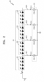
- FIG. 4 is a circuit diagram showing a lighting apparatus 40 according to one or more embodiments
- FIG. 5 is a timing diagram showing an example of the operation of the lighting apparatus 40 according to one or more embodiments.
- the circuit diagram of FIG. 4 shows the lighting apparatus 40 including a current distributor 44.
- FIGS. 4 and 5 equal to the descriptions given above with reference to FIGS. 2 and 3 will be omitted.
- the lighting apparatus 40 may include an LED array 42, an LED driver 43, the current distributor 44, a first diode D1, and a second diode D2, and, as described above with reference to FIG. 1 , may further include a rectifier (not shown).
- the LED array 42 may receive the input voltage V IN and may include the first to fourth LED groups G1 to G4.
- the LED driver 43 may include first to third current sources CS1 to CS3 respectively connected to three nodes N41 to N43 respectively corresponding to the first to third LED groups G1 to G3 and may include a fourth current source CS4 connected to the fourth LED group G4 through a plurality of nodes.
- the first to fourth current sources CS1 to CS4 may generate the first to fourth LED driving currents I DRV1 to I DRV4 in an enabled state, respectively.
- the first to fourth LED driving currents I DRV1 to I DRV4 may sequentially increase or have the same magnitude (I DRV1 ⁇ I DRV2 ⁇ I DRV3 ⁇ I DRV4 ).
- the LED driver 43 may include first to fourth switches SW1 to SW4 respectively corresponding to first to fourth LEDs L1 to L4 included in the fourth LED group G4. As shown in FIG. 4 , the first to fourth switches SW1 to SW4 may pass first to fourth currents IL 1 to IL 4 therethrough in the on-state, respectively. As described later with reference to FIG. 5 , the first to fourth switches SW1 to SW4 may be sequentially turned on or off according to the magnitude of the input voltage V IN , similarly as the first to fourth current sources CS1 to CS4.
- the current distributor 44 may be connected to LEDs included in the fourth LED group G4.
- the current distributor 44 may be connected to the first to fourth LEDs L1 to L4.
- the current distributor 44 may sense a second LED current IL 2 passing through a second LED L2, and, based on the sensed second LED current IL 2 , and may supply a third LED current IL 3 and a fourth LED current IL 4 to a third LED L3 and a fourth LED L4, respectively. Therefore, even when the input voltage V IN does not rise to the LED voltage V LED applied to the third LED L3 and the fourth LED L4 of the fourth LED group G4, the third LED L3 and the fourth LED L4 may emit light.
- a first terminal T1 of the current distributor 44 may be connected to a third LED group G3, and the current distributor 44 may supply a first LED current I L1 to a first LED L1.
- the current distributor 44 may sense the first LED current I L1 and supply second to fourth LED currents I L2 to I L4 based on the first LED current I L1 .
- the first terminal T1 of the current distributor 44 may be connected to the second LED L2. In this case, the current distributor 44 may sense the third LED current I L3 and supply the fourth LED current I L4 based on the third LED current I L3 .
- the input voltage V IN having a second peak PK2 may be provided to the LED array 42.
- the input voltage V IN may be greater than the LED voltage V LED applied to the first to third LED groups G1 to G3 and first to third LEDs L1 to L3 of the fourth LED group G4, but the input voltage V IN may not rise to the LED voltage V LED applied to the fourth LED L4. Nevertheless, the fourth LED L4 may emit light together with the second LED L2 and the third LED L3.
- the input voltage V IN may be higher than a LED voltage V LED applied to the first LED group G1, and only the first current source CS1 may be enabled. Therefore, the LED driving current I DRV may be equal to the first LED driving current I DRV1 , and, as shown in FIG. 3 , the first LED group G1 may emit light.
- the input voltage V IN may be higher than the LED voltage V LED applied to the first LED group G1 and the second LED group G2, and only the second current source CS2 may be enabled. Therefore, the LED driving current I DRV may be equal to the second LED driving current I DRV2 , and, as shown in FIG. 3 , the first LED group G1 and the second LED group G2 may emit light.
- the input voltage V IN may be higher than the LED voltage V LED applied to the first to third LED groups G1 to G3, and only the third current source C3 may be enabled.
- the LED driving current I DRV may be equal to the third LED driving current I DRV3 , and thus, as shown in FIG. 3 , the first to third LED groups G1 to G3 may emit light.
- the input voltage V IN may be higher than the LED voltage V LED applied to the first to third LED groups G1 to G3 and first LEDs L1 of the fourth LED group G4, and only a fourth current source C4 may be enabled.
- the LED driving current I DRV equal to a fourth LED driving current I DRV4 may pass through the first LED L1 and the first switch SW1, and the first LED current I L1 of FIG. 4 may be equal to the fourth LED driving current I DRV4 .
- the input voltage V IN may be higher than the LED voltage V LED applied to the first to third LED groups G1 to G3 and first LEDs L1 and second LEDs L2 of the fourth LED group G4, and only a fourth current source C4 may be enabled.
- the first switch SW1 may be turned off, and second to fourth switches SW2 to SW4 may maintain a turned-on state. Therefore, the LED driving current I DRV corresponding to the fourth LED driving current I DRV4 may pass through the first LED L1 and may flow while being dispersed in second to fourth LEDs L2 to L4.
- the fourth LED driving current I DRV4 may be equal to the first LED current I L1 and may be equal to the sum of the second to fourth LED currents I L2 to I L4 . Therefore, second to fourth LED currents I L2 to I L4 may flow in the second to fourth LEDs L2 to L4, respectively, and the second to fourth LEDs L2 to L4 may emit light.
- the input voltage V IN may be higher than the LED voltage V LED applied to the first to third LED groups G1 to G3 and the first to third LEDs L1 to L3 of the fourth LED group G4, and only the fourth current source C4 may be enabled.
- the first switch SW1 and a second switch SW2 may be turned off, and a third switch SW3 and a fourth switch SW4 may maintain a turn-on state. Therefore, the LED driving current I DRV equal to the fourth LED driving current I DRV4 may sequentially pass through the first LED L1 and the second LED L2 and may flow while being dispersed in the third LED L3 and the fourth LED L4.
- the fourth LED driving current I DRV4 may be equal to each of the first LED current I L1 and the second LED current I L2 and may be equal to the sum of the third LED current I L3 and the fourth LED current I L4 . Therefore, the third LED current I L3 and the fourth LED current I L4 may flow in the third LED L3 and the fourth LED L4, respectively, and the third LED L3 and the fourth LED L4 may emit light.
- the current distributor 44 for distributing current to the second to fourth LEDs L2 to L4 as shown in FIG. 5 will be described with reference to the drawings. However, one or more embodiments are not limited thereto, and the magnitudes of distributed currents may be variously combined by, for example, circuits described later with reference to FIGS. 10A to 10E .
- FIG. 6 is a circuit diagram showing a lighting apparatus 60 according to one or more embodiments
- FIG. 7 is a timing diagram showing the operation of the lighting apparatus 60 according to one or more embodiments.
- the lighting apparatus 60 may include an LED driver 63, a current distributor 64, the fourth LED group G4, the first diode D1, and the second diode D2.
- the fourth LED group G4 may include the first to fourth LEDs L1 to L4.
- the LED driver 63 may include the fourth current source CS4 and first to fourth transistors M61 to M64.
- the fourth current source CS4 may correspond to the fourth current source CS4 of FIG. 4
- the first to fourth transistors M61 to M64 may correspond to the first to fourth switches SW1 to SW4 of FIG. 4 , respectively.
- first to fourth voltages V1 to V4 may be applied to gates of the first to fourth transistors M61 to M64, respectively.
- the first to fourth voltages V1 to V4 may have sequentially increasing magnitudes (V1 ⁇ ⁇ V2 ⁇ V3 ⁇ V4), such that the first to fourth transistors M61 to M64 operate as described above with reference to FIG. 5 .
- V1 ⁇ ⁇ V2 ⁇ V3 ⁇ V4 sequentially increasing magnitudes
- the LED driver 63 may further include additional current sources.
- the LED driver 63 shown in FIG. 6 is merely an example, and, in some embodiments, the LED driver 63 may have a structure different from that shown in FIG. 6 (e.g., 83 of FIG. 8 ).
- the current distributor 64 may include the first terminal T1, a first current source CS61, and a second current source CS62.
- the first current source CS61 and the second current source CS62 may be current controlled current sources.
- a sensing voltage V SEN may be generated by sensing the second LED current I L2 passing through the second LED L2, that is, a first current I 1
- the first current source CS61 and the second current source CS62 may supply a second current I 2 and a third current I 3 corresponding to the magnitude of the sensing voltage V SEN .
- the first current source CS61 and the second current source CS62 respectively supply the second current I 2 and the third current I 3 having the same magnitude as the first current I 1 , but one or more embodiments are not limited thereto.
- the input voltage V IN may gradually increase.
- the input voltage V IN may cross a first threshold value THR 1 .
- the first threshold value THR 1 may correspond to the LED voltage of the first to third LED groups G1 to G3 and the LED voltage of the first LED L1 of the fourth LED group G4.
- the first to fourth transistors M61 to M64 are in the turned-on state, only the first LED L1 may be turned on due to the magnitude of the input voltage V IN , and thus the first LED current I L1 equal to the fourth LED driving current I DRV4 may pass through the first LED L1.
- the input voltage V IN may cross a second threshold value THR 2 .
- the second threshold value THR 2 may correspond to the LED voltage of the first to third LED groups G1 to G3 and the LED voltage of the first LED L1 and the second LED L2 of the fourth LED group G4.
- a first transistor M61 may be turned off, and second to fourth transistors M62 to M64 may maintain a turned-on state.
- the first LED current I L1 equal to the fourth LED driving current I DRV4 may flow into the current distributor 64 through the first terminal T1, and the sum of the second to fourth LED currents I L2 to I L4 may be equal to the first LED current I L1 .
- the first current source CS61 and the second current source CS62 may supply the second current I 2 and the third current I 3 having the same magnitude as the first current I 1 , respectively, and thus the second to fourth LED currents I L2 to I L4 may each correspond to 1/3 of the fourth LED driving current I DRV4 .
- the input voltage V IN may cross a third threshold value THR 3 .
- the third threshold value THR 3 may correspond to the LED voltage of the first to third LED groups G1 to G3 and the LED voltage of the first to third LEDs L1 to L3 of the fourth LED group G4.
- the first transistor M61 and a second transistor M62 may be turned off, and a third transistor M63 and a fourth transistor M64 may maintain a turned-on state.
- the third LED current I L3 may correspond to the sum of the second LED current I L2 (i.e., the first current I 1 ) and the second current I 2 supplied by the first current source CS61, and thus the third LED current I L3 may correspond to 2/3 of the fourth LED driving current I DRV4 .
- the input voltage V IN may cross a fourth threshold value THR 4 .
- the fourth threshold value THR 4 may correspond to the LED voltage of the first to third LED groups G1 to G3 and the LED voltage of the first to fourth LEDs L1 to L4 of the fourth LED group G4.
- First to third transistors M61 to M63 may be turned off, and the fourth transistor M64 may be turned on.
- the fourth LED current I L4 may correspond to the sum of the third LED current I L3 and the third current I 3 supplied by the second current source CS62, and thus the fourth LED current I L4 may correspond to the magnitude of the fourth LED driving current I DRV4 .
- currents may flow in all of the first to fourth LEDs L1 to L4 after the time point t41, and thus the first to fourth LEDs L1 to L4 may emit light.
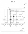
- FIG. 8 is a circuit diagram showing a lighting apparatus 80 according to one or more embodiments
- FIG. 9 is a timing diagram showing the operation of the lighting apparatus 80 according to one or more embodiments.
- the lighting apparatus 80 may include an LED driver 83, a current distributor 84, the fourth LED group G4, the first diode D1, and the second diode D2.
- the fourth LED group G4 may include the first to fourth LEDs L1 to L4.
- the LED driver 83 may include an amplifier A8, first to fourth transistors M81 to M84, diodes D81 to D83, and a resistor R8.
- the amplifier A8 may include a non-inverting input to which a reference voltage V REF is applied and an inverting input connected to the resistor R8 and provide a bias voltage VBIAS to gates of the first to fourth transistors M81 to M84. Therefore, the fourth current source CS4 that drains the fourth LED driving current I DRV4 having a magnitude corresponding to 'V REF /R8' from the fourth LED group G4 may be formed.
- an increasing drain-source voltage may be applied to the first to fourth transistors M81 to M84 by the diodes D81 to D83, and thus the first to fourth transistors M81 to M84 may correspond to the first to fourth switches SW1 to SW4 of FIG. 4 , respectively.
- the LED driver 83 may further include additional current sources.
- the LED driver 83 shown in FIG. 8 is merely an example, and, in some embodiments, the LED driver 83 may have a structure different from that shown in FIG. 8 (e.g., 63 of FIG. 6 ).
- the current distributor 84 may include the first terminal T1, a first current source CS81, and a second current source CS82.
- the first current source CS81 and the second current source CS82 may be current controlled current sources.
- a first sensing voltage V SEN1 may be generated by sensing the second LED current I L2 passing through the second LED L2, and the first current source CS81 may supply the second current I 2 corresponding to the magnitude of the first sensing voltage V SEN1 .
- a second sensing voltage V SEN2 may be generated by sensing the third LED current I L3 passing through the third LED L3, and the second current source CS82 may supply the third current I 3 corresponding to the magnitude of the second sensing voltage VSEN2.
- the input voltage V IN may gradually increase.
- the input voltage V IN may cross the first threshold value THR 1 .
- the first threshold value THR 1 may correspond to the LED voltage of the first to third LED groups G1 to G3 and the LED voltage of the first LED L1 of the fourth LED group G4.
- the first to fourth transistors M81 to M84 may be turned on.
- second to fourth transistors M82 to M84 may not pass current therethrough. Accordingly, the first LED current I L1 equal to the fourth LED driving current I DRV4 may pass through the first LED L1.
- the input voltage V IN may cross a second threshold value THR 2 .
- the second threshold value THR 2 may correspond to the LED voltage of the first to third LED groups G1 to G3 and the LED voltage of the first LED L1 and the second LED L2 of the fourth LED group G4.
- a first transistor M81 may be turned off, and the second to fourth transistors M82 to M84 may be turned on.
- the first LED current I L1 equal to the fourth LED driving current I DRV4 may flow into the current distributor 84 through the first terminal T1, and the sum of the second to fourth LED currents I L2 to I L4 may be equal to the first LED current I L1 .
- the first current source CS81 may supply the second current I 2 having the same magnitude as the first current I 1
- the second current source CS82 may supply the third current I 3 having the same magnitude as the third LED current I L3 . Therefore, the second LED current I L2 may correspond to 1/2 of the fourth LED driving current I DRV4 , respectively, the third LED current I L3 and the fourth LED current I L4 may each correspond to 1/4 of the fourth LED driving current I DRV4 .
- the input voltage V IN may cross the third threshold value THR 3 .
- the third threshold value THR 3 may correspond to the LED voltage of the first to third LED groups G1 to G3 and the LED voltage of the first to third LEDs L1 to L3 of the fourth LED group G4.
- the first transistor M81 and a second transistor M82 may be turned off, and a third transistor M83 and a fourth transistor M84 may be turned on.
- the third LED current I L3 may correspond to the sum of the second LED current I L2 and the second current I 2 supplied by the first current source CS81
- the magnitude of the fourth LED current I L4 may correspond to the magnitude of the third LED current I L3
- the sum of the third LED current I L3 and the fourth LED current I L4 may correspond to the fourth LED driving current I DRV4 . Therefore, the second LED current I L2 may correspond to 1/2 of the fourth LED driving current I DRV4
- the third LED current I L3 and the fourth LED current I L4 may each correspond to 1/2 of the fourth LED driving current I DRV4 .
- the input voltage V IN may cross the fourth threshold value THR 4 .
- the fourth threshold value THR 4 may correspond to the LED voltage of the first to third LED groups G1 to G3 and the LED voltage of the first to fourth LEDs L1 to L4 of the fourth LED group G4.
- First to third transistors M81 to M83 may be turned off, and the fourth transistor M84 may be turned on.
- the fourth LED current I L4 may correspond to the fourth LED driving current I DRV4
- the second LED current I L2 and the third LED current I L3 may each correspond to 1/2 of the fourth LED current I L4 .
- currents may flow in all of the first to fourth LEDs L1 to L4 after the time point t52, and thus the first to fourth LEDs L1 to L4 may emit light.
- FIGS. 10A to 10E are circuit diagrams showing examples of a current distributor according to one or more embodiments.
- FIGS. 10A to 10E show examples of a circuit included in a current distributor, which senses a sensing current I SEN and generates an output current I OUT based on the sensing current I SEN .
- a current distributor may include a current mirror.
- a circuit 10a may include a current mirror implemented with bipolar junction transistors. The output current I OUT passing through a second transistor Q2 may be proportional to the sensing current I SEN passing through a first transistor Q1.
- a circuit 10b may include a first resistor R1 and a second resistor R2 as well as a first transistor Q1 and a second transistor Q2.
- a circuit 10c may include a current mirror implemented with field effect transistors.
- the output current I OUT passing through a second transistor M2 may be proportional to the sensing current I SEN passing through a first transistor M1.
- a circuit 10d may include the first resistor R1 and the second resistor R2 as well as a first transistor M1 and a second transistor M2. Due to the first resistor R1 and the second resistor R2, an effect due to a mismatch between the first transistor M1 and the second transistor M2 may be reduced, and a ratio between the sensing current IsEN and the output current I OUT may be adjusted.
- a current distributor may include an amplifier.
- a circuit 10e may include an amplifier A10, the first transistor Q1, the first resistor R1, and the second resistor R2. Therefore, a voltage depending on the sensing current I SEN may be formed at a non-inverting input and an inverting input of the amplifier A10, and the output current I OUT having a magnitude dependent on the sensing current I SEN may be generated.
- the first transistor Q1 of the circuit 10e may be replaced with a field effect transistor (i.e., a PFET).
- a current distributor may include additional circuits in a manner similar to circuits shown in FIGS. 10A to 10E .
- the current distributor 64 of FIG. 6 may be implemented by adding a third transistor having a base connected to bases of the first transistor Q1 and the second transistor Q2 and an emitter connected to emitters of the first transistor Q1 and the second transistor Q2 to the circuit 10a of FIG. 10A . Therefore, the first current I 1 may correspond to the sensing current I SEN , and the second current I 2 and the third current I 3 may correspond to currents output by the second transistor Q2 and the added transistor, respectively. Also, the current distributor 64 of FIG.
- the first current I 1 may correspond to the sensing current I SEN
- the second current I 2 and the third current I 3 may correspond to currents output by the first transistor Q1 and the added transistor, respectively.
- FIG. 11 is a block diagram showing a lighting apparatus 110 according to one or more embodiments
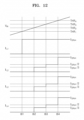
- FIG. 12 is a timing diagram showing the operation of the lighting apparatus 110 according to one or more embodiments.
- the lighting apparatus 110 may include an LED driver 113, a current distributor 114, the fourth LED group G4, the first diode D1, and the second diode D2.
- the LED driver 113 may include the fourth current source CS4 and the first to fourth switches SW1 to SW4.
- the current distributor 114 of FIG. 11 may be connected to anodes of the first diode D1 and the second diode D2.
- the input voltage V IN has a magnitude large enough to drive an LED
- at least a portion of the current distributor 114 may be disabled, thereby reducing power consumption by the current distributor 114 and providing higher current to the LED.
- the current distributor 114 may sense a voltage across the first diode D1 and a voltage across the second diode D2 and, when the voltage at an anode is higher than a voltage at a cathode, at least a portion of the current distributor 114 may be disabled.
- the input voltage V IN may gradually increase.
- the input voltage V IN may cross the first threshold value THR 1 .
- the first threshold value THR 1 may correspond to the LED voltage of the first to third LED groups G1 to G3 and the LED voltage of the first LED L1 of the fourth LED group G4.
- the first to fourth switches SW1 to SW4 may be turned on.
- the second to fourth switches SW2 to SW4 may not pass current therethrough. Accordingly, the first LED current I L1 equal to the fourth LED driving current I DRV4 may pass through the first LED L1.
- the input voltage V IN may cross a second threshold value THR 2 .
- the second threshold value THR 2 may correspond to the LED voltage of the first to third LED groups G1 to G3 and the LED voltage of the first LED L1 and the second LED L2 of the fourth LED group G4.
- the first switch SW1 may be turned off, and the second to fourth switches SW2 to SW4 may be turned on.
- the first LED current I L1 equal to the fourth LED driving current I DRV4 may flow into the current distributor 114 through the first terminal T1, and the sum of the second to fourth LED currents I L2 to I L4 may be equal to the first LED current I L1 . Therefore, the second to fourth LED currents IL2 to I L4 may each correspond to 1/3 of the fourth LED driving current I DRV4 .
- the input voltage V IN may cross the third threshold value THR 3 .
- the third threshold value THR 3 may correspond to the LED voltage of the first to third LED groups G1 to G3 and the LED voltage of the first to third LEDs L1 to L3 of the fourth LED group G4.
- the first switch SW1 and the second switch SW2 may be turned off, and a third switch SW3 and the fourth switch SW4 may be turned on.
- the second LED current I L2 may pass through the first diode D1 and constitute a part of the third LED current I L3 , and an anode voltage of the first diode D1 may be higher than a cathode voltage of the first diode D1.
- the current distributor 114 may disable a component that supplies a current based on the second LED current I L2 (e.g., CS61 of FIG. 6 or CS81 of FIG. 8 ), and thus the second LED current I L2 the third LED current I L3 may be equal to each other.
- the second to fourth LED currents IL2 to I L4 may correspond to 1/2 of the fourth LED driving current I DRV4 .
- the input voltage V IN may cross the fourth threshold value THR 4 .
- the fourth threshold value THR 4 may correspond to the LED voltage of the first to third LED groups G1 to G3 and the LED voltage of the first to fourth LEDs L1 to L4 of the fourth LED group G4.
- First to third switches SW1 to SW3 may be turned off, and the fourth switch SW4 may be turned on.
- the third LED current I L3 may pass through the second diode D2 and constitute a part of the fourth LED current I L4 , and an anode voltage of the second diode D2 may be higher than a cathode voltage of the second diode D2.
- the current distributor 114 may disable a component that supplies a current based on the third LED current I L3 (e.g., CS62 of FIG. 6 or CS82 of FIG. 8 ), and thus the second to fourth LED currents I L2 to I L4 may be equal to one another.
- the second to fourth LED currents IL2 to I L4 may correspond to the fourth LED driving current I DRV4 .
- currents having larger magnitudes may pass through the second to fourth LEDs L2 to L4, and thus light of stronger intensity may be emitted.
- FIG. 13 is a circuit diagram showing a current distributor 130 according to one or more embodiments.
- the circuit diagram of FIG. 13 shows the current distributor 130 for disabling a portion of the current distributor by sensing a voltage across a diode, as described above with reference to FIGS. 11 and 12 .
- the current distributor 130 includes first to fifth terminals T131 to T135, an amplifier A13, a comparator C13, a first transistor M131, a second transistor M132, a first resistor R131, and a second resistor R132.
- the first resistor R131 and/or the second resistor R132 may be provided outside the current distributor 130.
- the comparator C13 may receive a voltage across a diode D. When an anode voltage of the diode D is lower than a cathode voltage thereof, the comparator C13 may generate a high-level output signal. In response to the high-level output signal, the second transistor M132 may be turned off, and the amplifier A13, the first transistor M131, the first resistor R131, and the second resistor R132 may, as described above with reference to FIG. 10E , generate an output current I OUT that is dependent on the sensing current I SEN . Conversely, when the anode voltage of the diode D is higher than the cathode voltage thereof, the comparator C13 may generate a low-level output signal.
- the second transistor M132 may be turned on and electrically connect a source and a gate of the first transistor M131. Therefore, the first transistor M131 may be turned off, and the supply of a first output voltage I OUT may be cut off. It will be understood that the structure of FIG. 13 may be repeated when a current distributor distributes a plurality of currents, as described above with reference to FIGS. 10A to 10E .
- FIGS. 14A and 14B are block diagrams showing examples of a lighting apparatus according to one or more embodiments.
- a lighting apparatus 140a may include a plurality of current distributors, and the plurality of current distributors may be variously combined.
- the lighting apparatus 140a may include first to fourth current distributors 141a to 144a, the first to fourth LED groups G1 to G4, diodes D, and an LED driver 145a.
- the first to fourth current distributors 141a to 144a may be respectively included in four semiconductor packages or two or more current distributors from among the first to fourth current distributors 141a to 144a may be included in one semiconductor package.
- the first to fourth current distributors 141a to 144a may have the same structure.
- the first to fourth current distributors 141a to 144a may correspond to the first to fourth LED groups G1 to G4, respectively.
- the first to fourth current distributors 141a to 144a may each distribute a current to each of LEDs included in a corresponding LED group. Therefore, a time period during which LEDs of the first to fourth LED groups G1 to G4 emit light may be extended. Furthermore, despite the fluctuation of the peak of the input voltage V IN , all of LEDs in the first to fourth LED groups G1 to G4 may emit light.
- the first to fourth current distributors 141a to 144a may be connected to the anodes of the diodes D, respectively, and may disable at least some components based on voltages across the diodes D.
- a lighting apparatus 140b may include first to third current distributors 141b to 143b, the first to fourth LED groups G1 to G4, first to third diodes D1 to D3, and an LED driver 145b.
- the first to third current distributors 141b to 143b may be included in three semiconductor packages, respectively, or two or more current distributors from among the first to third current distributors 141b to 143b may be included in one semiconductor package.
- the first to third current distributors 141b to 143b may have the same structure.
- the first to third current distributors 141b to 143b may be connected in a cascaded shape.
- a first current distributor 141b may receive the LED driving current I DRV , and supply a first LED group current I G1 to the first LED group G1, and may sense the first LED group current I G1 and supply a first output current I OUT1 to a second current distributor 142b.
- the second current distributor 142b may receive the first output current I OUT1 and a current passed through the first diode D1, and supply a second LED group current I G2 to the second LED group G2, and may sense the second LED group current I G2 and supply a second output current I OUT2 to a third current distributor 143b.
- the third current distributor 143b may receive the second output current I OUT2 and a current passed through the second diode D2, and supply a third LED group current I G3 to the third LED group G3, and may sense the third LED group current I G3 and supply a third output current I OUT3 to the fourth LED group G4.
- the fourth LED group G4 may receive the third output current I OUT3 and a current passed through a third diode D3. Therefore, a time period during which LEDs of the first to fourth LED groups G1 to G4 emit light may be extended. Furthermore, despite the fluctuation of the peak of the input voltage V IN , all of LEDs in the first to fourth LED groups G1 to G4 may emit light.
- the first current distributor 141b may sense a voltage across the first diode D1 and may disable some components based on a sensed voltage.
- the second current distributor 142b may sense a voltage across the second diode D2 and may disable some components based on a sensed voltage.
- the third current distributor 143b may sense a voltage across the third diode D3 and may disable some components based on a sensed voltage.
- FIG. 15 is a flowchart of a method of driving an LED according to one or more embodiments.
- the method of driving an LED may include a plurality of operations S20, S40, and S60, and operations S40 and S60 may be performed in parallel with each other.
- the method of FIG. 15 may be performed by the LED driver 43 and current distributor 44 of FIG. 4 , which will be described below with reference to FIGS. 15 and 4 .
- the input voltage V IN rectified from the AC voltage V AC may be supplied to the LED array 42.
- the rectifier 11 of FIG. 1 may full-wave rectify the AC voltage V AC , and a full-wave rectified input voltage V IN may be supplied to the LED array 42.
- the LED driving current I DRV may be distributed in the fourth LED group G4.
- the fourth LED group G4 may be farthest apart from a node to which the input voltage V IN is applied. Even when the peak of the input voltage V IN fluctuates, the current distributor 44 may distribute a current to the first to fourth LEDs L1 to L4, such that the first to fourth LEDs L1 to L4 included in the fourth LED group G4 emit light. Examples of operation S40 will be described later with reference to FIGS. 16A and 16B .
- the LED driving current I DRV may be drained from the LED array 42.
- the LED driver 43 may include the first to fourth current sources CS1 to CS4 respectively corresponding to the first to fourth LED groups G1 to G4 included in the LED array 42, and the first to fourth current sources CS1 to CS4 may drain the first to fourth LED driving currents I DRV1 to I DRV4 from the LED array 42 in different periods, respectively.
- the fourth current source CS4 may drain the fourth LED driving current I DRV4 from the fourth LED group G4, and thus, in operation S40, the current distributor 44 may distribute the fourth LED driving current I DRV4 to the first to fourth LEDs L1 to L4 included in the fourth LED group G4.
- An example of operation S60 will be described later with reference to FIG. 17 .
- FIGS. 16A and 16B are flowcharts showing examples of a method of driving an LED according to one or more embodiments.
- the flowcharts of FIGS. 16A and 16B show examples of operation S40 of FIG. 15 , respectively.
- a LED driving current may be distributed in a fourth LED group.
- operation S40a of FIG. 16A may be performed by the current distributor 64 of FIG. 6
- operation S40b of FIG. 16B may be performed by the current distributor 84 of FIG. 8 .
- FIGS. 16A and 16B will be described with reference to FIGS. 6 and 8 .
- operation S40a may include a plurality of operations S41 to S43.
- operation S41 the first current I 1 passing through the second LED L2 may be sensed.
- the current distributor 64 of FIG. 6 may generate the sensing voltage V SEN by sensing the first current I 1 .
- the second current I 2 may be supplied to the third LED L3 based on the first LED current I L1 .
- the current distributor 64 may include the first current source CS61, and the first current source CS61 may supply the second current I 2 depending on the sensing voltage V SEN generated in operation S41 to the third LED L3.
- the third current I 3 may be supplied to the fourth LED L4 based on the first current I 1 .
- the current distributor 64 may include the second current source CS62, and the second current source CS62 may supply the third current I 3 depending on the sensing voltage V SEN generated in operation S41 to the fourth LED L4.
- operation S40b may include a plurality of operations S44 to S47.
- the first current I 1 passing through the second LED L2 may be sensed.
- the current distributor 84 of FIG. 8 may generate the first sensing voltage V SEN1 by sensing the first current I 1 .
- the second current I 2 may be supplied to the third LED L3 based on the first current I 1 .
- the current distributor 84 may include the first current source CS81, and the first current source CS81 may supply the second current I 2 depending on the first sensing voltage V SEN1 generated in operation S44 to the third LED L3.
- the third LED current I L3 passing through the third LED L3 may be sensed.
- the current distributor 84 of FIG. 8 may generate the second sensing voltage VSEN 2 by sensing the third LED current I L3 .
- the third current I 3 may be supplied to the fourth LED L4 based on the third LED current I L3 .
- the current distributor 84 may include the second current source CS82, and the second current source CS82 may supply the third current I 3 depending on the second sensing voltage V SEN2 generated in operation S46 to the fourth LED L4.
- FIG. 17 is a flowchart of a method of driving an LED according to one or more embodiments.
- FIG. 17 shows an example of operation S60 of FIG. 15 .
- an LED driving current may be drained from an LED array.
- operation S60' may include a plurality of operations S61 to S66.
- operation S60' may be performed by the LED driver 43 of FIG. 4 , and FIG. 17 will be described below with reference to FIG. 4 .
- the fourth current source CS4 may be connected to the second to fourth LEDs L2 to L4.
- the first switch SW1 may be turned off, and the second to fourth switches SW2 to SW4 may be turned on.
- the fourth current source CS4 may be disconnected from the second LED L2 and connected to the third LED L3 and the fourth LED L4.
- the first switch SW1 and the second switch SW2 may be turned off, and a third switch SW3 and the fourth switch SW4 may be turned on.
- the fourth current source CS4 may be disconnected from the second LED L2 and the third LED L3 and may be connected to the fourth LED L4.
- all LEDs included in the lighting apparatus may be driven even when the peak of an AC voltage fluctuates, and thus high LED utilization may be achieved.
- high light efficiency may be achieved in the lighting apparatus due to the high LED utilization.
Landscapes
- Circuit Arrangement For Electric Light Sources In General (AREA)
- Led Devices (AREA)
Applications Claiming Priority (1)
| Application Number | Priority Date | Filing Date | Title |
|---|---|---|---|
| KR1020210148957A KR102382016B1 (ko) | 2021-11-02 | 2021-11-02 | 높은 led 활용도를 제공하는 장치 및 이를 포함하는 조명 기기 |
Publications (1)
| Publication Number | Publication Date |
|---|---|
| EP4175420A1 true EP4175420A1 (fr) | 2023-05-03 |
Family
ID=81182713
Family Applications (1)
| Application Number | Title | Priority Date | Filing Date |
|---|---|---|---|
| EP22183665.3A Withdrawn EP4175420A1 (fr) | 2021-11-02 | 2022-07-07 | Dispositif de commande de del fournissant l'utilisation élevée de del et appareil d'éclairage comprenant un tel dispositif |
Country Status (5)
| Country | Link |
|---|---|
| US (1) | US11632841B1 (fr) |
| EP (1) | EP4175420A1 (fr) |
| JP (1) | JP2023068615A (fr) |
| KR (1) | KR102382016B1 (fr) |
| CN (1) | CN116075011B (fr) |
Citations (2)
| Publication number | Priority date | Publication date | Assignee | Title |
|---|---|---|---|---|
| US20160050730A1 (en) * | 2014-08-13 | 2016-02-18 | Gtc Co., Ltd. | Apparatus for Driving Light Emitting Diode Having A Current Switch |
| WO2016129855A1 (fr) * | 2015-02-13 | 2016-08-18 | 주식회사 실리콘웍스 | Dispositif d'éclairage |
Family Cites Families (10)
| Publication number | Priority date | Publication date | Assignee | Title |
|---|---|---|---|---|
| JP2005266397A (ja) * | 2004-03-19 | 2005-09-29 | Tohoku Pioneer Corp | 発光素子の駆動装置および駆動方法 |
| JP4945918B2 (ja) * | 2005-04-21 | 2012-06-06 | ソニー株式会社 | Led駆動装置 |
| US9226364B2 (en) | 2010-10-28 | 2015-12-29 | Citizen Holdings Co., Ltd. | LED lighting circuit, LED illumination device, and LED illumination unit socket |
| KR102011068B1 (ko) * | 2011-05-06 | 2019-08-14 | 이동일 | Led 구동 장치 및 이를 이용한 led 구동 방법 |
| TWI441560B (zh) * | 2011-06-30 | 2014-06-11 | Interlight Optotech Corp | 發光二極體模組及其操作方法 |
| KR101940780B1 (ko) | 2011-09-16 | 2019-01-22 | 서울반도체 주식회사 | 반도체 발광 소자를 적용한 조명 장치 |
| KR102091197B1 (ko) * | 2012-12-18 | 2020-03-18 | 엘지디스플레이 주식회사 | 발광다이오드 어레이 구동장치 및 이를 이용한 액정표시장치 |
| CN105282929B (zh) * | 2015-10-20 | 2018-04-27 | 晨辉光宝科技有限公司 | 一种自动切换模式的全电压分段式线性恒流led驱动电路 |
| CN107094329B (zh) * | 2017-05-03 | 2019-01-29 | 矽力杰半导体技术(杭州)有限公司 | Led驱动电路 |
| KR102296219B1 (ko) * | 2020-12-21 | 2021-09-01 | 주식회사 웰랑 | 조명 기기의 부품에 전력을 공급하기 위한 장치 및 이를 포함하는 조광가능 조명 기기 |
-
2021
- 2021-11-02 KR KR1020210148957A patent/KR102382016B1/ko active Active
-
2022
- 2022-07-06 JP JP2022109003A patent/JP2023068615A/ja active Pending
- 2022-07-07 EP EP22183665.3A patent/EP4175420A1/fr not_active Withdrawn
- 2022-07-08 CN CN202210805552.4A patent/CN116075011B/zh active Active
- 2022-07-08 US US17/860,656 patent/US11632841B1/en active Active
Patent Citations (2)
| Publication number | Priority date | Publication date | Assignee | Title |
|---|---|---|---|---|
| US20160050730A1 (en) * | 2014-08-13 | 2016-02-18 | Gtc Co., Ltd. | Apparatus for Driving Light Emitting Diode Having A Current Switch |
| WO2016129855A1 (fr) * | 2015-02-13 | 2016-08-18 | 주식회사 실리콘웍스 | Dispositif d'éclairage |
Also Published As
| Publication number | Publication date |
|---|---|
| CN116075011A (zh) | 2023-05-05 |
| CN116075011B (zh) | 2024-02-23 |
| KR102382016B1 (ko) | 2022-04-04 |
| US20230132682A1 (en) | 2023-05-04 |
| US11632841B1 (en) | 2023-04-18 |
| JP2023068615A (ja) | 2023-05-17 |
Similar Documents
| Publication | Publication Date | Title |
|---|---|---|
| JP5091567B2 (ja) | 発光素子の駆動回路および電子機器 | |
| US8941325B2 (en) | Light emitting device array driver circuit and current splitter circuit and method of splitting current therefor | |
| US8248000B2 (en) | Light emitting device driver circuit, light emitting device array controller and control method thereof | |
| TWI477187B (zh) | 適應性切換模式發光二極體系統 | |
| CN111613185B (zh) | 发光元件驱动装置、发光元件驱动系统及发光系统 | |
| KR20050006042A (ko) | 부하 구동 장치 및 휴대 기기 | |
| KR102648750B1 (ko) | 화소 및 이를 포함하는 표시 장치 | |
| US20110266962A1 (en) | Driver ic for electrical load and driving method thereof | |
| US8884545B2 (en) | LED driving system and driving method thereof | |
| KR20130018065A (ko) | 엘이디 구동회로 | |
| CN112585670A (zh) | 驱动电路、其驱动方法及显示装置 | |
| KR101247506B1 (ko) | 엘이디 스트링의 구동 장치 | |
| US8633922B2 (en) | Power supplying apparatus for organic light emitting display | |
| US20100052572A1 (en) | Light emitting element driving apparatus | |
| JP2006320158A (ja) | 定電流駆動回路、それを利用した電子機器および発光ダイオードの駆動方法 | |
| US20070001652A1 (en) | Multi-power supply circuit and multi-power supply method | |
| EP4175420A1 (fr) | Dispositif de commande de del fournissant l'utilisation élevée de del et appareil d'éclairage comprenant un tel dispositif | |
| KR101400606B1 (ko) | 엘이디 조명 구동회로 | |
| CN107135569B (zh) | 用于照明装置的控制电路 | |
| US7948480B2 (en) | Current driving circuit | |
| CN102665323B (zh) | 发光二极管串的驱动方法、驱动电路及其驱动方法 | |
| US20240179812A1 (en) | Linear driving module | |
| KR100707615B1 (ko) | 유기 전계발광 표시장치의 직류-직류 컨버터 | |
| JP7097049B2 (ja) | 発光ダイオードの駆動回路 | |
| KR20090068103A (ko) | Led 구동장치 |
Legal Events
| Date | Code | Title | Description |
|---|---|---|---|
| PUAI | Public reference made under article 153(3) epc to a published international application that has entered the european phase |
Free format text: ORIGINAL CODE: 0009012 |
|
| STAA | Information on the status of an ep patent application or granted ep patent |
Free format text: STATUS: REQUEST FOR EXAMINATION WAS MADE |
|
| 17P | Request for examination filed |
Effective date: 20220707 |
|
| AK | Designated contracting states |
Kind code of ref document: A1 Designated state(s): AL AT BE BG CH CY CZ DE DK EE ES FI FR GB GR HR HU IE IS IT LI LT LU LV MC MK MT NL NO PL PT RO RS SE SI SK SM TR |
|
| STAA | Information on the status of an ep patent application or granted ep patent |
Free format text: STATUS: EXAMINATION IS IN PROGRESS |
|
| 17Q | First examination report despatched |
Effective date: 20240115 |
|
| GRAP | Despatch of communication of intention to grant a patent |
Free format text: ORIGINAL CODE: EPIDOSNIGR1 |
|
| STAA | Information on the status of an ep patent application or granted ep patent |
Free format text: STATUS: GRANT OF PATENT IS INTENDED |
|
| INTG | Intention to grant announced |
Effective date: 20250224 |
|
| STAA | Information on the status of an ep patent application or granted ep patent |
Free format text: STATUS: THE APPLICATION IS DEEMED TO BE WITHDRAWN |
|
| 18D | Application deemed to be withdrawn |
Effective date: 20250625 |