EP4177622A1 - Leck- und ladedetektorschaltung - Google Patents
Leck- und ladedetektorschaltung Download PDFInfo
- Publication number
- EP4177622A1 EP4177622A1 EP22202257.6A EP22202257A EP4177622A1 EP 4177622 A1 EP4177622 A1 EP 4177622A1 EP 22202257 A EP22202257 A EP 22202257A EP 4177622 A1 EP4177622 A1 EP 4177622A1
- Authority
- EP
- European Patent Office
- Prior art keywords
- voltage
- comparator
- sampling capacitor
- output
- switch
- Prior art date
- Legal status (The legal status is an assumption and is not a legal conclusion. Google has not performed a legal analysis and makes no representation as to the accuracy of the status listed.)
- Granted
Links
Images


Classifications
-
- G—PHYSICS
- G01—MEASURING; TESTING
- G01R—MEASURING ELECTRIC VARIABLES; MEASURING MAGNETIC VARIABLES
- G01R31/00—Arrangements for testing electric properties; Arrangements for locating electric faults; Arrangements for electrical testing characterised by what is being tested not provided for elsewhere
- G01R31/50—Testing of electric apparatus, lines, cables or components for short-circuits, continuity, leakage current or incorrect line connections
- G01R31/52—Testing for short-circuits, leakage current or ground faults
-
- A—HUMAN NECESSITIES
- A61—MEDICAL OR VETERINARY SCIENCE; HYGIENE
- A61B—DIAGNOSIS; SURGERY; IDENTIFICATION
- A61B5/00—Measuring for diagnostic purposes; Identification of persons
- A61B5/145—Measuring characteristics of blood in vivo, e.g. gas concentration or pH-value ; Measuring characteristics of body fluids or tissues, e.g. interstitial fluid or cerebral tissue
- A61B5/1468—Measuring characteristics of blood in vivo, e.g. gas concentration or pH-value ; Measuring characteristics of body fluids or tissues, e.g. interstitial fluid or cerebral tissue using chemical or electrochemical methods, e.g. by polarographic means
-
- A—HUMAN NECESSITIES
- A61—MEDICAL OR VETERINARY SCIENCE; HYGIENE
- A61B—DIAGNOSIS; SURGERY; IDENTIFICATION
- A61B5/00—Measuring for diagnostic purposes; Identification of persons
- A61B5/72—Signal processing specially adapted for physiological signals or for diagnostic purposes
- A61B5/7225—Details of analogue processing, e.g. isolation amplifier, gain or sensitivity adjustment, filtering, baseline or drift compensation
-
- G—PHYSICS
- G01—MEASURING; TESTING
- G01R—MEASURING ELECTRIC VARIABLES; MEASURING MAGNETIC VARIABLES
- G01R19/00—Arrangements for measuring currents or voltages or for indicating presence or sign thereof
- G01R19/165—Indicating that current or voltage is either above or below a predetermined value or within or outside a predetermined range of values
- G01R19/16566—Circuits and arrangements for comparing voltage or current with one or several thresholds and for indicating the result not covered by subgroups G01R19/16504, G01R19/16528, G01R19/16533
- G01R19/1659—Circuits and arrangements for comparing voltage or current with one or several thresholds and for indicating the result not covered by subgroups G01R19/16504, G01R19/16528, G01R19/16533 to indicate that the value is within or outside a predetermined range of values (window)
-
- G—PHYSICS
- G01—MEASURING; TESTING
- G01R—MEASURING ELECTRIC VARIABLES; MEASURING MAGNETIC VARIABLES
- G01R31/00—Arrangements for testing electric properties; Arrangements for locating electric faults; Arrangements for electrical testing characterised by what is being tested not provided for elsewhere
- G01R31/50—Testing of electric apparatus, lines, cables or components for short-circuits, continuity, leakage current or incorrect line connections
- G01R31/66—Testing of connections, e.g. of plugs or non-disconnectable joints
- G01R31/68—Testing of releasable connections, e.g. of terminals mounted on a printed circuit board
-
- A—HUMAN NECESSITIES
- A61—MEDICAL OR VETERINARY SCIENCE; HYGIENE
- A61B—DIAGNOSIS; SURGERY; IDENTIFICATION
- A61B5/00—Measuring for diagnostic purposes; Identification of persons
- A61B5/145—Measuring characteristics of blood in vivo, e.g. gas concentration or pH-value ; Measuring characteristics of body fluids or tissues, e.g. interstitial fluid or cerebral tissue
- A61B5/14532—Measuring characteristics of blood in vivo, e.g. gas concentration or pH-value ; Measuring characteristics of body fluids or tissues, e.g. interstitial fluid or cerebral tissue for measuring glucose, e.g. by tissue impedance measurement
-
- A—HUMAN NECESSITIES
- A61—MEDICAL OR VETERINARY SCIENCE; HYGIENE
- A61B—DIAGNOSIS; SURGERY; IDENTIFICATION
- A61B5/00—Measuring for diagnostic purposes; Identification of persons
- A61B5/145—Measuring characteristics of blood in vivo, e.g. gas concentration or pH-value ; Measuring characteristics of body fluids or tissues, e.g. interstitial fluid or cerebral tissue
- A61B5/1468—Measuring characteristics of blood in vivo, e.g. gas concentration or pH-value ; Measuring characteristics of body fluids or tissues, e.g. interstitial fluid or cerebral tissue using chemical or electrochemical methods, e.g. by polarographic means
- A61B5/1477—Measuring characteristics of blood in vivo, e.g. gas concentration or pH-value ; Measuring characteristics of body fluids or tissues, e.g. interstitial fluid or cerebral tissue using chemical or electrochemical methods, e.g. by polarographic means non-invasive
Definitions
- Various exemplary embodiments disclosed herein relate generally to a circuit that monitors its external terminals to detect current leakage when nothing is connected to the circuit or the presence of a load between terminals of the circuit.
- a detector circuit including: a voltage source configured to produce a first voltage on a first output, a second voltage on a second output, and third voltage on a third output, wherein the first voltage is greater than the second voltage and the second voltage is greater than the third voltage; a first switch connected to the second output; a sampling capacitor connected to the switch, wherein the sampling capacitor is charged by the voltage source when the switch is closed; a first comparator with one input connected to the first output and a second input connected to the sampling capacitor; a second comparator with one input connected to the third output and a second input connected to the sampling capacitor; a multiplexer with a plurality of inputs configured to be connected to a plurality of terminals of an external circuit and an output connected to the sampling capacitor, the first input of the first comparator, and the first input of the second comparator; and a controller with inputs connected to the first comparator, the second comparator, and a clock generation unit, wherein the controller is configured to produce control signals to control the first switch and the
- a sensor system including: a sensor; and a sensor interface circuit including a detector circuit including: a voltage source configured to produce a first voltage on a first output, a second voltage on a second output, and third voltage on a third output, wherein the first voltage is greater than the second voltage and the second voltage is greater than the third voltage; a first switch connected to the second output; a sampling capacitor connected to the switch, wherein the sampling capacitor is charged by the voltage source when the switch is closed; a first comparator with one input connected to the first output and a second input connected to the sampling capacitor; a second comparator with one input connected to the third output and a second input connected to the sampling capacitor; a multiplexer with a plurality of inputs configured to be connected to a plurality of terminals of an external circuit and an output connected to the sampling capacitor, the first input of the first comparator, and the first input of the second comparator; and a controller with inputs connected to the first comparator, the second comparator, and a clock generation unit,
- the voltage source includes a bandgap voltage source and a bandgap buffer.
- control signals produced by the controller include signals to control the plurality of additional switches.
- controller is configured to: close the first switch to charge the sampling capacitor; connect one of the plurality terminals to the sampling capacitor using the multiplexer; open the first switch; and monitor the outputs of the first comparator and the second comparator to determine if there is a current leak on the connected terminal.
- controller is further configured to measure the leakage current.
- the output signal further indicates a connection to the external circuit.
- the controller is configured to: connect all but one of the plurality of terminals to ground using the plurality of additional switches; close the first switch to charge the sampling capacitor; open the first switch; connect one terminal not connected to ground to the sampling capacitor using the multiplexer; and monitor the outputs of the first comparator and the second comparator to determine if the detection circuit is connected to the external circuit.
- controller is further configured to measure a resistance of the external circuit.
- the output signal indicates a connection to the external circuit when a voltage on the sampling capacitor drops below the third voltage.
- the output signal indicates the presence of a current leak when a voltage on the sampling capacitor drops below the third voltage.
- FIG. 1 For various embodiments, relate to a method for detecting a current leak in an external circuit using a detector circuit, including: producing a first voltage on a first output of a voltage source, a second voltage on a second output of a voltage source, and third voltage on a third output of a voltage source, wherein the first voltage is greater than the second voltage and the second voltage is greater than the third voltage; charging a sampling capacitor using the second voltage by closing a switch connected between the sampling capacitor and the voltage source; opening the first switch; comparing a voltage on the sampling capacitor with the first output; comparing a voltage on the sampling capacitor with the second output; selecting one of a plurality of inputs configured to be connected to a plurality of terminals of an external circuit; connecting the selected input to the sampling capacitor; producing control signals, by a controller, to control the first switch and the selecting one of a plurality of inputs; and producing an output signal indicting the presence of a current leak on one of the plurality of terminals.
- the output signal further indicates a connection to the external circuit.
- Various embodiments are described, further including; connecting all but one of the plurality of terminals to ground using the plurality of additional switches; closing the first switch to charge the sampling capacitor; opening the first switch; connecting one terminal not connected to ground to the sampling capacitor using the multiplexer; and monitoring the outputs of the first comparator and the second comparator to determine if the detection circuit is connected to the external circuit.
- Various embodiments are described, further including measuring, by the controller, a resistance of the external circuit.
- the output signal indicates a connection to the external circuit when a voltage on the sampling capacitor drops below the third voltage.
- the output signal indicates the presence of a current leak when a voltage on the sampling capacitor drops below the third voltage.
- a monitoring circuit may be used to measure a pad/node leakage during production testing. Further, once the electrochemical sensor is placed in use, the monitoring circuit may verify that the electrochemical sensor has been successfully connected and is operating.
- One example of such an electrochemical sensor is a continuous glucose monitoring sensor.
- a continuous glucose monitoring (CGM) sensor is hydrated and then variations in the glucose level may be measured through terminals of the chip interfacing the CGM sensor so that the glucose level may be monitored.
- the CGM sensor may include three terminals: CE; RE, and WE.
- the circuit interfacing the CGM sensor may also have CE, RE, and WE terminals.
- the RE terminal is a reference electrode of the sensor that maintains a constant reference voltage for WE electrode.
- the WE terminal is a work electrode of the sensor where the electrochemical reaction occurs, hence the current is generated and read.
- the CE terminal is a counter electrode of the sensor that is a connection to the electrolyte for current to compensate for reaction at the WE terminal.
- the current reading of a CGM circuit needs to be accurate to a few pA, and potential leakage on the RE pin can damage the sensor. During production, each of these terminals may be tested to determine if the terminal has any current leakage in order to prevent damage to the CGM sensor via leakage at the RE terminal.
- a detector circuit is described herein that may be used to detect current leakage of the various terminals of a circuit. Further, the detector circuit may be able to monitor the sensor during use to verify that it is properly connected and loaded, i.e., hydrated in the case of a CGM sensor.
- the detector circuit described herein will avoid the use of expensive and complex analog to digital circuits and other such circuits to result in a detector circuit that is accurate and inexpensive to implement.
- a glucose monitoring circuit with three terminals is used as an example herein, but other types of circuits or sensors that requires leakage detection during production and/or determining the connection and operation of the circuit during use. Further, the detection circuit described herein may be used with circuits that have any number of terminals that need to be monitored.
- FIG. 1 illustrates a diagram of a detection circuit that may be used to detect current leakage and connectivity between pins in a circuit.
- the monitored system is a CGM system where the leakage of a CGM readout circuit and the hydration of the CGM sensor are detected.
- the detection circuit 100 includes a bandgap voltage reference 102, bandgap buffer 104, sampling capacitor C s 106, first comparator 108, second comparator 110, controller 112, clock generation unit 114, and a mux 116.
- the bandgap voltage reference 102 produces three output voltages: V bg and V bg +/- ⁇ V.
- the voltage V bg is buffered by the bandgap buffer 104 to isolate the bandgap voltage from the sampling capacitor C s 106 as the sensor capacitance can be much larger than the integrated Cs, and in that case the bandgap voltage may jump down when connected to the empty parasitic capacitor.
- the bandgap buffer 104 is implemented with an operational amplifier, but other implementations may be used as well.
- the switch 118 is connected between the bandgap buffer 104 and the sampling capacitor C s 106. When the switch 118 is closed the buffered bandgap voltage V bg is sampled by charging the sampling capacitor C s 106.
- the switch 118 may be controlled by a control signal 126 output by the controller 112.
- the switch 118 may be implemented using any type of switch typically used in electrical circuits.
- the first comparator 108 receives V bg + ⁇ V as one input and the sampling capacitor voltage V cap as the other input. The output of the first comparator 108 indicates whether the sampling capacitor voltage V cap is above or below V bg + ⁇ V.
- the second comparator 110 receives V bg - ⁇ V as one input and the sampling capacitor voltage V cap as the other input. The output of the second comparator 110 indicates whether the sampling capacitor voltage V cap is above or below V bg - ⁇ V.
- the comparators 108, 110 may be implemented using operational amplifiers or any other typically used circuit.
- the controller 112 receives the outputs of the first comparator 108 and the second comparator 112 and a clock signal from the clock generation unit 114.
- the controller 112 produces various control signals 126 that are used to control the MUX 116 and the various switches 118, 120, 122, 124.
- the operation of the controller 112 will be further described below.
- the controller 112 may be implemented using a small programable microcontroller, a processor, a state machine, or dedicated logic that implements the desired control features and steps.
- the MUX 116 is connected to the three terminals CE 130, RE 132, and WE 134 of a chip interfacing the CGM sensor.
- the output of the MUX 116 is connected to a node between the sampling capacitor C s 106 and the first comparator 108 and the second comparator 110.
- the MUX 116 receives a control signal 126 from the controller 112 that controls which of the three inputs (i.e., CE 130, RE 132, and WE 134) if any are connected to the output of the MUX 116.
- the MUX 116 is shown as having three inputs, but the MUX 116 may have fewer or more inputs depending upon the number of inputs that the circuit to be monitored has.
- the switches 120, 122, 124 are connected to the terminals 130, 132, 134.
- the switches 120, 122, 124 are also connected to ground which is designated as VSS, so that when any of the switches 120, 122, 124 are closed, the corresponding terminal is connected to ground.
- Three switches are illustrated, but fewer or more switches may be used depending upon the number of circuit inputs that need to be monitored.
- the detection circuit 100 has two modes of operation including a leakage current detection mode and a sensor connection and/or hydration mode.
- the leakage current detection mode may be used during production to detect if any of the terminals of the chip exhibit excessive current leakage.
- the sensor connection and/or hydration mode may be used to detect that the sensor is properly connected and/or properly hydrated (as in the case of a CGM sensor).
- FIG. 2 illustrates the operation of the detection circuit during the leakage current detection mode.
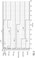
- FIG. 3 illustrates plots of various voltages and control signals in the detection circuit during the leakage current detection mode.
- the leakage current detection mode includes the following steps: open the switches 120, 122, 124 connecting the terminals CE 130, RE 132, and WE 134 to ground; sample the bandgap voltage on sampling capacitor C s 106 by closing switch 118; connect the terminal to be measured to C s by using the MUX 116; and open the switch 118 and then the controller 112 monitors the comparator outputs for a period of time. This process may be repeated for each of the terminals as needed.
- FIG. 2 illustrates a current leakage source 140 connected to the WE terminal 134.
- the leakage source will cause the sense capacitor voltage V cap to decrease or increase over time.
- the output of the first comparator 108 will indicate that the sense capacitor voltage C cap is now greater than V bg + ⁇ V or the output of the second comparator 110 will indicate that the sense capacitor voltage C cap is now less than V bg - ⁇ V after a certain time interval based upon the clock signal from the clock generation unit.
- the programmable parameter ⁇ t may be fixed by the controller. Note that this circuit can detect both leakage current polarities on a node, i.e., a current flowing into the sense capacitor C s 106 or a current flowing out of the sense capacitor C s 106.
- FIG. 3 includes plots of the voltages V bg + ⁇ V 302, V cap 304, and V bg - ⁇ V 306. Further, plots of the output for the first comparator 308 and the second comparator 310 are illustrated. A plot of an enable signal 312 that is used to enable the operation of the detection circuit is also illustrated. A plot of a control signal connect_vref 314 illustrates the time when the switch 118 is closed to charge the sampling capacitor C s 106. Finally, a control signal connect_sensor 316 illustrates the time when the MUX 116 connects one of the terminals 130, 132, 134 to the sampling capacitor C s 106. When the enable signal 312 goes high the detection circuit can begin to operate.
- V cap is 0V so the output of the second comparator 110 goes high because V cap is below V bg - ⁇ V.
- the output 308 of the first comparator remains zero because V cap is below V bg + ⁇ V except for startup artifacts which will be digitally gated out.
- the signal connect_ref 314 goes high to close the switch 118 for a period of time so that the sampling capacitor C s 106 is charged.
- the connect_sensor signal 316 goes high to enable the MUX 116 to connect one of the terminals to be tested to the sampling capacitor C s 106.
- V cap 304 increases to the value of V bg that causes the output 310 of the second comparator to become low because V cap is now above V bg - ⁇ V.
- Vcap decreases because of a current leak
- the controller may indicate to a user or testing apparatus that the pin being tested has a current leak.
- the enable signal 312 goes low, which disables the detection circuit so the output 310 of the second comparator goes low.
- one of the switches 120, 122, 124 corresponding to the terminal being tested may be closed to ground the sampling capacitor C s 106 to discharge it so that its output 304 goes to 0 V. In other embodiments this may not be done in order to save power.
- FIG. 4 illustrates the operation of the detection circuit during the sensor connection and/or hydration mode.
- FIG. 5 illustrates plots of various voltages and control signals in the detection circuit during the sensor connection and/or hydration mode.
- the sensor connection and/or hydration mode includes the following steps: connect the CE terminal 130 and the WE terminal 134 to ground; sample the bandgap voltage on sampling capacitor C s 106 by closing switch 118; connect the RE terminal 132 to the sampling capacitor C s 106 using the MUX 116 and then open the switch 118; and monitor the comparator outputs using the controller 112 for a period of time to determine if V cap decays indicating connection and/or hydration and to determine a load resistance value R if desired.
- a hydrated CGM sensor connected between WE and RE will create an impedance to ground in parallel to the discharging sampling capacitor C s 106.
- a maximum impedance can be measured by defining a programmable time interval after opening the switch 118 and the voltage difference ⁇ V on the output of the second comparator 110.
- V cap V bg e ⁇ t RC s ) .
- V cap at a specific time t, will allow the value of R to be calculated. This value then can be used to determine if the sensor is connected and is properly operating/hydrated.
- FIG. 5 includes plots of voltages at voltages V bg + ⁇ V 510, V cap 512, and V bg - ⁇ V 514.
- a plot of a control signal enable_and_ground_CE_WE 504 is shown that indicates when the terminals CE 130 and WE 134 are grounded, and the detection circuit is enabled.
- a plot of a control signal connect_vref 506 illustrates the time when the switch 118 is closed to charge the sampling capacitor C s 106.
- a control signal connect_sensor 508 illustrates the time when the MUX 116 connects the RE terminal 132 to the sampling capacitor C s 106.
- a plot of the output 502 of the first comparator 108 and the output 516 of the second comparator 110 are illustrated.
- the enablesignal 504 goes high, the terminals CE 130 and WE 134 are grounded. This causes the voltage at the CE terminal 130 and WE terminal 134 to be grounded and go to 0 V. Further, at this point the output 516 of the second comparator 110 will go high indicating that V cap 512 is below V bg - ⁇ V 514.
- the signal connect_vref 506 goes high to close the switch 118 for a period of time so that the sampling capacitor C s 106 is charged. This results in V cap 514 increasing to the voltage level of V bg , and the output of the second comparator 110 will go low indicating that V cap 512 is above V bg - ⁇ V 514.
- the connect_sensor signal 508 goes high to enable the MUX 116 to connect the RE terminal 132 to the sampling capacitor C s 106.
- the value of Vcap decreases because the charge on the sampling capacitor 106 is dissipated in the resistance R (as described by the equation above), and once V cap 512 decreases below V bg - ⁇ V 514, the output 516 of the second comparator goes high. This indicates to the controller 112 that the sensor is connected and/or hydrated. Based upon the voltage change and the amount of time taken to result in the voltage change, a value for R may be calculated as described above.
- the enable signal 504 can then go low to disable the operation of the detection circuit.
- V bg and ⁇ V may be programmable and allow for the ability to detect a wide range of leakage currents and resistance values.
- the detection circuit described herein may effectively measure the leakage of a node/pad during chip or integrated circuit (IC) test production to help identified faulty samples to be discarded or to detect a finite impedance between two electrodes in order to wake-up more power consuming sensor readout circuitry during application.
- the detection circuit does not require any ADC or complex circuitry. Further the detection circuit can be easily calibrated, and it can be programmed for a wide range of leakage currents and resistance values.
- a detector circuit including: a voltage source configured to produce a first voltage on a first output, a second voltage on a second output, and third voltage on a third output, wherein the first voltage is greater than the second voltage and the second voltage is greater than the third voltage; a first switch connected to the second output; a sampling capacitor connected to the switch, wherein the sampling capacitor is charged by the voltage source when the switch is closed; a first comparator with one input connected to the first output and a second input connected to the sampling capacitor; a second comparator with one input connected to the third output and a second input connected to the sampling capacitor; a multiplexer with a plurality of inputs configured to be connected to a plurality of terminals of an external circuit and an output connected to the sampling capacitor, the first input of the first comparator, and the first input of the second comparator; and a controller with inputs connected to the first comparator, the second comparator, and a clock generation unit, wherein the controller is configured to produce control signals to control the first switch and the
Landscapes
- Health & Medical Sciences (AREA)
- Physics & Mathematics (AREA)
- Life Sciences & Earth Sciences (AREA)
- General Physics & Mathematics (AREA)
- Engineering & Computer Science (AREA)
- Animal Behavior & Ethology (AREA)
- Public Health (AREA)
- Pathology (AREA)
- Veterinary Medicine (AREA)
- Biomedical Technology (AREA)
- Heart & Thoracic Surgery (AREA)
- Medical Informatics (AREA)
- Molecular Biology (AREA)
- Surgery (AREA)
- Biophysics (AREA)
- General Health & Medical Sciences (AREA)
- Optics & Photonics (AREA)
- Signal Processing (AREA)
- Emergency Medicine (AREA)
- Power Engineering (AREA)
- Artificial Intelligence (AREA)
- Computer Vision & Pattern Recognition (AREA)
- Physiology (AREA)
- Psychiatry (AREA)
- Chemical & Material Sciences (AREA)
- Chemical Kinetics & Catalysis (AREA)
- General Chemical & Material Sciences (AREA)
- Testing Of Short-Circuits, Discontinuities, Leakage, Or Incorrect Line Connections (AREA)
Applications Claiming Priority (1)
| Application Number | Priority Date | Filing Date | Title |
|---|---|---|---|
| US17/518,258 US11774517B2 (en) | 2021-11-03 | 2021-11-03 | Leakage and loading detector circuit |
Publications (2)
| Publication Number | Publication Date |
|---|---|
| EP4177622A1 true EP4177622A1 (de) | 2023-05-10 |
| EP4177622B1 EP4177622B1 (de) | 2024-07-10 |
Family
ID=83903213
Family Applications (1)
| Application Number | Title | Priority Date | Filing Date |
|---|---|---|---|
| EP22202257.6A Active EP4177622B1 (de) | 2021-11-03 | 2022-10-18 | Leck- und ladedetektorschaltung |
Country Status (3)
| Country | Link |
|---|---|
| US (1) | US11774517B2 (de) |
| EP (1) | EP4177622B1 (de) |
| CN (1) | CN116087824A (de) |
Families Citing this family (1)
| Publication number | Priority date | Publication date | Assignee | Title |
|---|---|---|---|---|
| US20260002976A1 (en) * | 2024-06-27 | 2026-01-01 | Cirrus Logic International Semiconductor Ltd. | Fault detection circuitry |
Citations (2)
| Publication number | Priority date | Publication date | Assignee | Title |
|---|---|---|---|---|
| US20090105571A1 (en) * | 2006-06-30 | 2009-04-23 | Abbott Diabetes Care, Inc. | Method and System for Providing Data Communication in Data Management Systems |
| US20190101585A1 (en) * | 2017-09-29 | 2019-04-04 | Infineon Technologies Ag | Evaluating a gate-source leakage current in a transistor device |
Family Cites Families (18)
| Publication number | Priority date | Publication date | Assignee | Title |
|---|---|---|---|---|
| US6426632B1 (en) * | 1999-03-29 | 2002-07-30 | George A. Spencer | Method and apparatus for testing an AFCI/GFCI circuit breaker |
| US6330697B1 (en) * | 1999-04-20 | 2001-12-11 | International Business Machines Corporation | Apparatus and method for performing a defect leakage screen test for memory devices |
| US6611146B2 (en) * | 2001-06-28 | 2003-08-26 | International Business Machines Corporation | Stress testing for semiconductor devices |
| JP2007172766A (ja) | 2005-12-22 | 2007-07-05 | Matsushita Electric Ind Co Ltd | 半導体リーク電流検出器とリーク電流測定方法および電圧トリミング機能付半導体リーク電流検出器とリファレンス電圧トリミング方法およびこれらの半導体集積回路 |
| US7985330B2 (en) | 2005-12-30 | 2011-07-26 | Medtronic Minimed, Inc. | Method and system for detecting age, hydration, and functional states of sensors using electrochemical impedance spectroscopy |
| US20070169533A1 (en) | 2005-12-30 | 2007-07-26 | Medtronic Minimed, Inc. | Methods and systems for detecting the hydration of sensors |
| US7928744B2 (en) * | 2008-12-02 | 2011-04-19 | Analog Devices, Inc. | Monitoring circuit having a self test function |
| US8588007B2 (en) * | 2011-02-28 | 2013-11-19 | Micron Technology, Inc. | Leakage measurement systems |
| US8634264B2 (en) * | 2011-10-26 | 2014-01-21 | Micron Technology, Inc. | Apparatuses, integrated circuits, and methods for measuring leakage current |
| KR102058577B1 (ko) * | 2013-09-13 | 2019-12-24 | 삼성디스플레이 주식회사 | 표시 장치 및 그 구동 방법 |
| US20150088438A1 (en) * | 2013-09-26 | 2015-03-26 | James J. Kinsella | Ratio metric current measurement |
| US9697912B2 (en) * | 2015-05-26 | 2017-07-04 | Micron Technology, Inc. | Leakage current detection |
| US9443610B1 (en) * | 2015-06-04 | 2016-09-13 | Micron Technology, Inc. | Leakage current detection |
| US10008276B2 (en) * | 2016-04-27 | 2018-06-26 | Sandisk Technologies Llc | High accuracy leakage detection through low voltage biasing |
| FR3071351B1 (fr) * | 2017-09-18 | 2019-08-30 | Airbus Operations (S.A.S.) | Liaison electrique comprenant un systeme de protection electrique |
| KR102343295B1 (ko) * | 2019-11-05 | 2021-12-24 | 현대모비스 주식회사 | 누설전류 검출 기능을 구비한 bms 반도체 장치 및 그것의 누설전류 검출 방법 |
| KR102714918B1 (ko) * | 2019-12-26 | 2024-10-11 | 에이엠에스 인터내셔널 에이쥐 | 센서 회로들 |
| US11402409B1 (en) * | 2021-03-22 | 2022-08-02 | Allegro Microsystems, Llc | Differential current sensor package |
-
2021
- 2021-11-03 US US17/518,258 patent/US11774517B2/en active Active
-
2022
- 2022-10-18 EP EP22202257.6A patent/EP4177622B1/de active Active
- 2022-11-03 CN CN202211381677.5A patent/CN116087824A/zh active Pending
Patent Citations (2)
| Publication number | Priority date | Publication date | Assignee | Title |
|---|---|---|---|---|
| US20090105571A1 (en) * | 2006-06-30 | 2009-04-23 | Abbott Diabetes Care, Inc. | Method and System for Providing Data Communication in Data Management Systems |
| US20190101585A1 (en) * | 2017-09-29 | 2019-04-04 | Infineon Technologies Ag | Evaluating a gate-source leakage current in a transistor device |
Also Published As
| Publication number | Publication date |
|---|---|
| US20230133063A1 (en) | 2023-05-04 |
| CN116087824A (zh) | 2023-05-09 |
| EP4177622B1 (de) | 2024-07-10 |
| US11774517B2 (en) | 2023-10-03 |
Similar Documents
| Publication | Publication Date | Title |
|---|---|---|
| US6456045B1 (en) | Integrated conductance and load test based electronic battery tester | |
| US6304087B1 (en) | Apparatus for calibrating electronic battery tester | |
| US4216424A (en) | Method and apparatus for testing electrolytic capacitors | |
| US9588180B2 (en) | Architecture and method to determine leakage impedance and leakage voltage node | |
| US5757192A (en) | Method and apparatus for detecting a bad cell in a storage battery | |
| US6806716B2 (en) | Electronic battery tester | |
| US6392414B2 (en) | Electronic battery tester | |
| US20020175687A1 (en) | Electronic Battery tester | |
| JP2004191373A (ja) | 電子バッテリテスタ | |
| US20130041606A1 (en) | Detecting an open wire between a battery cell and an external circuit | |
| US20050104604A1 (en) | Process and a circuit arrangement for evaluating a measuring capacitance | |
| JP2004294437A (ja) | 電子バッテリテスタ | |
| US11249117B2 (en) | Autoranging ammeter with fast dynamic response | |
| JP7217681B2 (ja) | 蓄電デバイスの測定装置及び測定方法 | |
| CN104865411A (zh) | 动态补偿电路 | |
| US20230198035A1 (en) | Measurement apparatus, and measurement method | |
| US11988717B2 (en) | Measurement apparatus of power storage device and measurement method | |
| CN113270909B (zh) | 用于管理电池系统的方法和装置 | |
| CN103052889B (zh) | 用于对输入偏置电流的高敏感度检测的系统及方法 | |
| EP4177622A1 (de) | Leck- und ladedetektorschaltung | |
| CN105785269A (zh) | 一种电池电量计量系统及方法 | |
| JP4825782B2 (ja) | 自動検査設備内部の寄生容量を精密に計測するシステム、回路および方法 | |
| CN111220901B (zh) | 运放测试系统和方法 | |
| JP6718284B2 (ja) | 信号処理回路、クーロンカウンタ回路、電子機器 | |
| JP7328820B2 (ja) | 蓄電デバイスの検査装置及び検査方法 |
Legal Events
| Date | Code | Title | Description |
|---|---|---|---|
| PUAI | Public reference made under article 153(3) epc to a published international application that has entered the european phase |
Free format text: ORIGINAL CODE: 0009012 |
|
| STAA | Information on the status of an ep patent application or granted ep patent |
Free format text: STATUS: THE APPLICATION HAS BEEN PUBLISHED |
|
| AK | Designated contracting states |
Kind code of ref document: A1 Designated state(s): AL AT BE BG CH CY CZ DE DK EE ES FI FR GB GR HR HU IE IS IT LI LT LU LV MC ME MK MT NL NO PL PT RO RS SE SI SK SM TR |
|
| STAA | Information on the status of an ep patent application or granted ep patent |
Free format text: STATUS: REQUEST FOR EXAMINATION WAS MADE |
|
| 17P | Request for examination filed |
Effective date: 20231110 |
|
| RBV | Designated contracting states (corrected) |
Designated state(s): AL AT BE BG CH CY CZ DE DK EE ES FI FR GB GR HR HU IE IS IT LI LT LU LV MC ME MK MT NL NO PL PT RO RS SE SI SK SM TR |
|
| GRAP | Despatch of communication of intention to grant a patent |
Free format text: ORIGINAL CODE: EPIDOSNIGR1 |
|
| STAA | Information on the status of an ep patent application or granted ep patent |
Free format text: STATUS: GRANT OF PATENT IS INTENDED |
|
| INTG | Intention to grant announced |
Effective date: 20240228 |
|
| GRAS | Grant fee paid |
Free format text: ORIGINAL CODE: EPIDOSNIGR3 |
|
| GRAA | (expected) grant |
Free format text: ORIGINAL CODE: 0009210 |
|
| STAA | Information on the status of an ep patent application or granted ep patent |
Free format text: STATUS: THE PATENT HAS BEEN GRANTED |
|
| AK | Designated contracting states |
Kind code of ref document: B1 Designated state(s): AL AT BE BG CH CY CZ DE DK EE ES FI FR GB GR HR HU IE IS IT LI LT LU LV MC ME MK MT NL NO PL PT RO RS SE SI SK SM TR |
|
| REG | Reference to a national code |
Ref country code: CH Ref legal event code: EP |
|
| REG | Reference to a national code |
Ref country code: DE Ref legal event code: R096 Ref document number: 602022004465 Country of ref document: DE |
|
| REG | Reference to a national code |
Ref country code: LT Ref legal event code: MG9D |
|
| REG | Reference to a national code |
Ref country code: NL Ref legal event code: MP Effective date: 20240710 |
|
| PG25 | Lapsed in a contracting state [announced via postgrant information from national office to epo] |
Ref country code: PT Free format text: LAPSE BECAUSE OF FAILURE TO SUBMIT A TRANSLATION OF THE DESCRIPTION OR TO PAY THE FEE WITHIN THE PRESCRIBED TIME-LIMIT Effective date: 20241111 |
|
| REG | Reference to a national code |
Ref country code: AT Ref legal event code: MK05 Ref document number: 1702500 Country of ref document: AT Kind code of ref document: T Effective date: 20240710 |
|
| PG25 | Lapsed in a contracting state [announced via postgrant information from national office to epo] |
Ref country code: NL Free format text: LAPSE BECAUSE OF FAILURE TO SUBMIT A TRANSLATION OF THE DESCRIPTION OR TO PAY THE FEE WITHIN THE PRESCRIBED TIME-LIMIT Effective date: 20240710 |
|
| PG25 | Lapsed in a contracting state [announced via postgrant information from national office to epo] |
Ref country code: PT Free format text: LAPSE BECAUSE OF FAILURE TO SUBMIT A TRANSLATION OF THE DESCRIPTION OR TO PAY THE FEE WITHIN THE PRESCRIBED TIME-LIMIT Effective date: 20241111 Ref country code: NL Free format text: LAPSE BECAUSE OF FAILURE TO SUBMIT A TRANSLATION OF THE DESCRIPTION OR TO PAY THE FEE WITHIN THE PRESCRIBED TIME-LIMIT Effective date: 20240710 |
|
| PG25 | Lapsed in a contracting state [announced via postgrant information from national office to epo] |
Ref country code: NO Free format text: LAPSE BECAUSE OF FAILURE TO SUBMIT A TRANSLATION OF THE DESCRIPTION OR TO PAY THE FEE WITHIN THE PRESCRIBED TIME-LIMIT Effective date: 20241010 |
|
| PG25 | Lapsed in a contracting state [announced via postgrant information from national office to epo] |
Ref country code: GR Free format text: LAPSE BECAUSE OF FAILURE TO SUBMIT A TRANSLATION OF THE DESCRIPTION OR TO PAY THE FEE WITHIN THE PRESCRIBED TIME-LIMIT Effective date: 20241011 Ref country code: FI Free format text: LAPSE BECAUSE OF FAILURE TO SUBMIT A TRANSLATION OF THE DESCRIPTION OR TO PAY THE FEE WITHIN THE PRESCRIBED TIME-LIMIT Effective date: 20240710 Ref country code: PL Free format text: LAPSE BECAUSE OF FAILURE TO SUBMIT A TRANSLATION OF THE DESCRIPTION OR TO PAY THE FEE WITHIN THE PRESCRIBED TIME-LIMIT Effective date: 20240710 |
|
| PG25 | Lapsed in a contracting state [announced via postgrant information from national office to epo] |
Ref country code: BG Free format text: LAPSE BECAUSE OF FAILURE TO SUBMIT A TRANSLATION OF THE DESCRIPTION OR TO PAY THE FEE WITHIN THE PRESCRIBED TIME-LIMIT Effective date: 20240710 |
|
| PG25 | Lapsed in a contracting state [announced via postgrant information from national office to epo] |
Ref country code: LV Free format text: LAPSE BECAUSE OF FAILURE TO SUBMIT A TRANSLATION OF THE DESCRIPTION OR TO PAY THE FEE WITHIN THE PRESCRIBED TIME-LIMIT Effective date: 20240710 |
|
| PG25 | Lapsed in a contracting state [announced via postgrant information from national office to epo] |
Ref country code: AT Free format text: LAPSE BECAUSE OF FAILURE TO SUBMIT A TRANSLATION OF THE DESCRIPTION OR TO PAY THE FEE WITHIN THE PRESCRIBED TIME-LIMIT Effective date: 20240710 Ref country code: IS Free format text: LAPSE BECAUSE OF FAILURE TO SUBMIT A TRANSLATION OF THE DESCRIPTION OR TO PAY THE FEE WITHIN THE PRESCRIBED TIME-LIMIT Effective date: 20241110 |
|
| PG25 | Lapsed in a contracting state [announced via postgrant information from national office to epo] |
Ref country code: HR Free format text: LAPSE BECAUSE OF FAILURE TO SUBMIT A TRANSLATION OF THE DESCRIPTION OR TO PAY THE FEE WITHIN THE PRESCRIBED TIME-LIMIT Effective date: 20240710 |
|
| PG25 | Lapsed in a contracting state [announced via postgrant information from national office to epo] |
Ref country code: ES Free format text: LAPSE BECAUSE OF FAILURE TO SUBMIT A TRANSLATION OF THE DESCRIPTION OR TO PAY THE FEE WITHIN THE PRESCRIBED TIME-LIMIT Effective date: 20240710 Ref country code: RS Free format text: LAPSE BECAUSE OF FAILURE TO SUBMIT A TRANSLATION OF THE DESCRIPTION OR TO PAY THE FEE WITHIN THE PRESCRIBED TIME-LIMIT Effective date: 20241010 |
|
| PG25 | Lapsed in a contracting state [announced via postgrant information from national office to epo] |
Ref country code: RS Free format text: LAPSE BECAUSE OF FAILURE TO SUBMIT A TRANSLATION OF THE DESCRIPTION OR TO PAY THE FEE WITHIN THE PRESCRIBED TIME-LIMIT Effective date: 20241010 Ref country code: PL Free format text: LAPSE BECAUSE OF FAILURE TO SUBMIT A TRANSLATION OF THE DESCRIPTION OR TO PAY THE FEE WITHIN THE PRESCRIBED TIME-LIMIT Effective date: 20240710 Ref country code: NO Free format text: LAPSE BECAUSE OF FAILURE TO SUBMIT A TRANSLATION OF THE DESCRIPTION OR TO PAY THE FEE WITHIN THE PRESCRIBED TIME-LIMIT Effective date: 20241010 Ref country code: LV Free format text: LAPSE BECAUSE OF FAILURE TO SUBMIT A TRANSLATION OF THE DESCRIPTION OR TO PAY THE FEE WITHIN THE PRESCRIBED TIME-LIMIT Effective date: 20240710 Ref country code: IS Free format text: LAPSE BECAUSE OF FAILURE TO SUBMIT A TRANSLATION OF THE DESCRIPTION OR TO PAY THE FEE WITHIN THE PRESCRIBED TIME-LIMIT Effective date: 20241110 Ref country code: HR Free format text: LAPSE BECAUSE OF FAILURE TO SUBMIT A TRANSLATION OF THE DESCRIPTION OR TO PAY THE FEE WITHIN THE PRESCRIBED TIME-LIMIT Effective date: 20240710 Ref country code: GR Free format text: LAPSE BECAUSE OF FAILURE TO SUBMIT A TRANSLATION OF THE DESCRIPTION OR TO PAY THE FEE WITHIN THE PRESCRIBED TIME-LIMIT Effective date: 20241011 Ref country code: FI Free format text: LAPSE BECAUSE OF FAILURE TO SUBMIT A TRANSLATION OF THE DESCRIPTION OR TO PAY THE FEE WITHIN THE PRESCRIBED TIME-LIMIT Effective date: 20240710 Ref country code: ES Free format text: LAPSE BECAUSE OF FAILURE TO SUBMIT A TRANSLATION OF THE DESCRIPTION OR TO PAY THE FEE WITHIN THE PRESCRIBED TIME-LIMIT Effective date: 20240710 Ref country code: BG Free format text: LAPSE BECAUSE OF FAILURE TO SUBMIT A TRANSLATION OF THE DESCRIPTION OR TO PAY THE FEE WITHIN THE PRESCRIBED TIME-LIMIT Effective date: 20240710 Ref country code: AT Free format text: LAPSE BECAUSE OF FAILURE TO SUBMIT A TRANSLATION OF THE DESCRIPTION OR TO PAY THE FEE WITHIN THE PRESCRIBED TIME-LIMIT Effective date: 20240710 |
|
| REG | Reference to a national code |
Ref country code: DE Ref legal event code: R097 Ref document number: 602022004465 Country of ref document: DE |
|
| PG25 | Lapsed in a contracting state [announced via postgrant information from national office to epo] |
Ref country code: SM Free format text: LAPSE BECAUSE OF FAILURE TO SUBMIT A TRANSLATION OF THE DESCRIPTION OR TO PAY THE FEE WITHIN THE PRESCRIBED TIME-LIMIT Effective date: 20240710 Ref country code: RO Free format text: LAPSE BECAUSE OF FAILURE TO SUBMIT A TRANSLATION OF THE DESCRIPTION OR TO PAY THE FEE WITHIN THE PRESCRIBED TIME-LIMIT Effective date: 20240710 Ref country code: DK Free format text: LAPSE BECAUSE OF FAILURE TO SUBMIT A TRANSLATION OF THE DESCRIPTION OR TO PAY THE FEE WITHIN THE PRESCRIBED TIME-LIMIT Effective date: 20240710 |
|
| PG25 | Lapsed in a contracting state [announced via postgrant information from national office to epo] |
Ref country code: EE Free format text: LAPSE BECAUSE OF FAILURE TO SUBMIT A TRANSLATION OF THE DESCRIPTION OR TO PAY THE FEE WITHIN THE PRESCRIBED TIME-LIMIT Effective date: 20240710 |
|
| PG25 | Lapsed in a contracting state [announced via postgrant information from national office to epo] |
Ref country code: CZ Free format text: LAPSE BECAUSE OF FAILURE TO SUBMIT A TRANSLATION OF THE DESCRIPTION OR TO PAY THE FEE WITHIN THE PRESCRIBED TIME-LIMIT Effective date: 20240710 |
|
| PG25 | Lapsed in a contracting state [announced via postgrant information from national office to epo] |
Ref country code: SK Free format text: LAPSE BECAUSE OF FAILURE TO SUBMIT A TRANSLATION OF THE DESCRIPTION OR TO PAY THE FEE WITHIN THE PRESCRIBED TIME-LIMIT Effective date: 20240710 Ref country code: IT Free format text: LAPSE BECAUSE OF FAILURE TO SUBMIT A TRANSLATION OF THE DESCRIPTION OR TO PAY THE FEE WITHIN THE PRESCRIBED TIME-LIMIT Effective date: 20240710 |
|
| PLBE | No opposition filed within time limit |
Free format text: ORIGINAL CODE: 0009261 |
|
| STAA | Information on the status of an ep patent application or granted ep patent |
Free format text: STATUS: NO OPPOSITION FILED WITHIN TIME LIMIT |
|
| 26N | No opposition filed |
Effective date: 20250411 |
|
| PG25 | Lapsed in a contracting state [announced via postgrant information from national office to epo] |
Ref country code: MC Free format text: LAPSE BECAUSE OF FAILURE TO SUBMIT A TRANSLATION OF THE DESCRIPTION OR TO PAY THE FEE WITHIN THE PRESCRIBED TIME-LIMIT Effective date: 20240710 |
|
| PG25 | Lapsed in a contracting state [announced via postgrant information from national office to epo] |
Ref country code: LU Free format text: LAPSE BECAUSE OF NON-PAYMENT OF DUE FEES Effective date: 20241018 Ref country code: BE Free format text: LAPSE BECAUSE OF NON-PAYMENT OF DUE FEES Effective date: 20241031 |
|
| PG25 | Lapsed in a contracting state [announced via postgrant information from national office to epo] |
Ref country code: FR Free format text: LAPSE BECAUSE OF NON-PAYMENT OF DUE FEES Effective date: 20241031 |
|
| P01 | Opt-out of the competence of the unified patent court (upc) registered |
Free format text: CASE NUMBER: APP_29983/2025 Effective date: 20250623 |
|
| REG | Reference to a national code |
Ref country code: BE Ref legal event code: MM Effective date: 20241031 |
|
| PG25 | Lapsed in a contracting state [announced via postgrant information from national office to epo] |
Ref country code: SE Free format text: LAPSE BECAUSE OF FAILURE TO SUBMIT A TRANSLATION OF THE DESCRIPTION OR TO PAY THE FEE WITHIN THE PRESCRIBED TIME-LIMIT Effective date: 20240710 |
|
| PG25 | Lapsed in a contracting state [announced via postgrant information from national office to epo] |
Ref country code: IE Free format text: LAPSE BECAUSE OF NON-PAYMENT OF DUE FEES Effective date: 20241018 |
|
| PGFP | Annual fee paid to national office [announced via postgrant information from national office to epo] |
Ref country code: DE Payment date: 20250923 Year of fee payment: 4 |
|
| PG25 | Lapsed in a contracting state [announced via postgrant information from national office to epo] |
Ref country code: CY Free format text: LAPSE BECAUSE OF FAILURE TO SUBMIT A TRANSLATION OF THE DESCRIPTION OR TO PAY THE FEE WITHIN THE PRESCRIBED TIME-LIMIT; INVALID AB INITIO Effective date: 20221018 |
|
| PG25 | Lapsed in a contracting state [announced via postgrant information from national office to epo] |
Ref country code: HU Free format text: LAPSE BECAUSE OF FAILURE TO SUBMIT A TRANSLATION OF THE DESCRIPTION OR TO PAY THE FEE WITHIN THE PRESCRIBED TIME-LIMIT; INVALID AB INITIO Effective date: 20221018 |