EP4177928B1 - Méthode de mesure de courant ionique en deux étapes dans un dispositif d'analyse de processus plasma - Google Patents
Méthode de mesure de courant ionique en deux étapes dans un dispositif d'analyse de processus plasma Download PDFInfo
- Publication number
- EP4177928B1 EP4177928B1 EP21207043.7A EP21207043A EP4177928B1 EP 4177928 B1 EP4177928 B1 EP 4177928B1 EP 21207043 A EP21207043 A EP 21207043A EP 4177928 B1 EP4177928 B1 EP 4177928B1
- Authority
- EP
- European Patent Office
- Prior art keywords
- voltage
- grid
- ion current
- ion
- plasma
- Prior art date
- Legal status (The legal status is an assumption and is not a legal conclusion. Google has not performed a legal analysis and makes no representation as to the accuracy of the status listed.)
- Active
Links
Images


Classifications
-
- H—ELECTRICITY
- H01—ELECTRIC ELEMENTS
- H01J—ELECTRIC DISCHARGE TUBES OR DISCHARGE LAMPS
- H01J37/00—Discharge tubes with provision for introducing objects or material to be exposed to the discharge, e.g. for the purpose of examination or processing thereof
- H01J37/32—Gas-filled discharge tubes
- H01J37/32917—Plasma diagnostics
- H01J37/32935—Monitoring and controlling tubes by information coming from the object and/or discharge
-
- H—ELECTRICITY
- H01—ELECTRIC ELEMENTS
- H01J—ELECTRIC DISCHARGE TUBES OR DISCHARGE LAMPS
- H01J37/00—Discharge tubes with provision for introducing objects or material to be exposed to the discharge, e.g. for the purpose of examination or processing thereof
- H01J37/32—Gas-filled discharge tubes
- H01J37/32917—Plasma diagnostics
-
- G—PHYSICS
- G01—MEASURING; TESTING
- G01T—MEASUREMENT OF NUCLEAR OR X-RADIATION
- G01T1/00—Measuring X-radiation, gamma radiation, corpuscular radiation, or cosmic radiation
- G01T1/36—Measuring spectral distribution of X-rays or of nuclear radiation spectrometry
- G01T1/366—Measuring spectral distribution of X-rays or of nuclear radiation spectrometry with semi-conductor detectors
-
- H—ELECTRICITY
- H01—ELECTRIC ELEMENTS
- H01J—ELECTRIC DISCHARGE TUBES OR DISCHARGE LAMPS
- H01J37/00—Discharge tubes with provision for introducing objects or material to be exposed to the discharge, e.g. for the purpose of examination or processing thereof
- H01J37/32—Gas-filled discharge tubes
- H01J37/32009—Arrangements for generation of plasma specially adapted for examination or treatment of objects, e.g. plasma sources
- H01J37/32422—Arrangement for selecting ions or species in the plasma
-
- H—ELECTRICITY
- H01—ELECTRIC ELEMENTS
- H01J—ELECTRIC DISCHARGE TUBES OR DISCHARGE LAMPS
- H01J49/00—Particle spectrometers or separator tubes
- H01J49/44—Energy spectrometers, e.g. alpha-, beta-spectrometers
- H01J49/46—Static spectrometers
- H01J49/48—Static spectrometers using electrostatic analysers, e.g. cylindrical sector, Wien filter
- H01J49/488—Static spectrometers using electrostatic analysers, e.g. cylindrical sector, Wien filter with retarding grids
-
- H—ELECTRICITY
- H01—ELECTRIC ELEMENTS
- H01J—ELECTRIC DISCHARGE TUBES OR DISCHARGE LAMPS
- H01J2237/00—Discharge tubes exposing object to beam, e.g. for analysis treatment, etching, imaging
- H01J2237/245—Detection characterised by the variable being measured
- H01J2237/24564—Measurements of electric or magnetic variables, e.g. voltage, current, frequency
Definitions
- the present application relates to a device for measuring the incident charged particle current densities and energy distributions arriving at a substrate or surface during plasma processing.
- Plasma processing is used extensively in modern industry for a wide range of applications.
- a well-known example is the manufacture of integrated circuits in the semiconductor industry.
- Plasma processing is also used in the production of solar panels, flat panel displays, thin film coatings and medical devices, among many others.
- the substrate is a silicon wafer while in other industries the substrate may be glass panel or a variety of alternatives.
- Wafer and substrate may be used interchangeably through the document but understood to mean any type of substrate to be used in a plasma process.
- the substrate surface is bombarded by plasma species, including energetic ions, to remove (etch) and/or deposit layers of material to form structures or features on the workpiece surface. Ion impact may drive the etching and deposition directly, or may be used to activate the surface for more reactive plasma species to do the work.
- the ion flux and associated (IED) determines important parameters such as etch rate, etch selectivity and etch anisotropy.
- the lED is therefore a critical plasma parameter to measure, understand and control to ensure optimum process performance.
- EP 3968354 A1 describes an apparatus for obtaining ion energy distribution measurements in a plasma processing system comprising a substrate for placement in the plasma processing system, an ion energy analyser disposed in the substrate for measuring the ion energy distribution at the substrate surface during plasma processing, the analyser comprising a first conductive grid, a second conductive grid, a third conductive grid, a fourth conductive grid, and a collection electrode, each grid separated by an insulating layer, a battery power supply and a battery manager integrated in the substrate, for supplying and controlling voltage to each of the grids and the collector of the ion energy analyser; and a high voltage generating circuit within the substrate, the high voltage generating circuit comprising a high voltage pulse generator feeding a voltage multiplier, wherein the high voltage generating circuit is configured to take the output voltage of the battery manager and supply a voltage sweep to the third conductive grid.
- the high voltage generating circuit of EP 3968354 A1 may be configured to generate a descending voltage sweep and the ion energy analyser configured to sample ion current while the voltage sweep is descending.
- EP 3971942 A1 belongs to the prior art according to Article 54(3) EPC.
- EP 3971942 A1 relates to an apparatus for obtaining ion energy distribution, IED, measurements in a plasma processing system comprising a substrate for placement in the plasma processing system and exposed to the plasma, an ion energy analyser disposed in the substrate for measuring the ion energy distribution at the substrate surface during plasma processing, the analyser comprising a first conductive grid, G0, a second conductive grid, G1, a third conductive grid, G2, a fourth conductive grid G3, and a collection electrode, C, each grid separated by an insulating layer, a battery power supply and a battery manager integrated in the substrate, for supplying and controlling voltage to each of the grids and the collector of the ion energy analyser, and a high voltage generating circuit within the substrate, wherein the high voltage generating circuit takes the output voltage of the battery manager and supplies a voltage sweep to the third conductive grid.
- US 2005/0115673 A1 relates to an imitation silicon substrate with a variety of integrated sensors including an ion energy analyzer, a VUV photon detector and a radical ion emission spectrophotometer.
- This device has a fully integrated power source and control electronics. Bi-direction communication with a viewport mounted receiver is performed optically.
- the ion energy analyzer consists of four grids including a plasma blocking grid, an incoming electron retarding grid, an ion energy separation grid and a secondary electron suppression grid. It also includes a collector electrode to record the current of ions as a function of ion energy. Grid layers and inter-grid isolation layers are present. Voltages are applied to each grid to create the electric fields required to operate the sensor.
- the present teachings provide a method of operating an apparatus to obtain ion energy distribution measurements in a plasma processing system, as defined in claim 1, comprising providing a substrate for placement in the plasma processing system and exposure to the plasma, the substrate having an ion energy analyser disposed therein for measuring the ion energy distribution at the substrate surface during plasma processing, the analyser comprising a plurality of conductive grids, and a collection electrode, C, each grid separated by an insulating layer, providing a high voltage generating circuit within the substrate and configured to take the output voltage of a battery to power the high voltage generating circuit and apply a voltage to a first grid of the plurality of conductive grids, providing a high voltage switch configured to discharge the first grid to a floating ground of the apparatus, and a resistor in parallel with the high voltage switch, sampling ion current during a first stage while a first voltage is being charged on the first grid from the floating ground potential to a plateau voltage, and sampling ion current during a second stage while a second voltage applied to the first grid is dis
- the method may further comprise closing the switch to discharge the first grid to the floating ground prior to sampling ion current during the first stage.
- the method may further comprise opening the switch to allow ion current from a plasma process to charge the first grid to the plateau voltage.
- the plateau voltage is determined by the ion current from the plasma process flowing through the resistor.
- the first voltage is an ascending voltage sweep and the second voltage is a descending voltage sweep.
- the high voltage circuit may comprise a voltage multiplier and the resistor is in parallel with the voltage multiplier.
- the resistance value of the resistor in parallel with the total capacitance to the floating ground of the voltage multiplier and the ion current may determine the rate at which the second voltage discharges.
- the resistance value of the resistor in parallel with the total capacitance to the floating ground of the voltage multiplier and the ion current determines the rate at which the first voltage charges.
- the method may further comprise combining the ion current sampled during the first stage with the ion current sampled during the second stage to obtain a complete set of measurements across the full ion energy distribution.
- the method may further comprise plotting the complete set of measurements to provide an ion energy distribution.
- the plurality of grids is arranged as a stack of conductive grids and the first grid is any one of the grids in the stack, the first grid being used for ion energy discrimination.
- the invention is defined by the claims.
- Figure 1 illustrates an overview of a system 100 that is capable of measuring the ion energy distribution arriving at the wafer probe 101 surface during plasma processing.
- the diagnostic system 100 includes an imitation wafer probe with integrated ion energy analysers, electronic control circuitry, battery power supply and wireless communication.
- the diagnostic system further comprises a docking station 102 with integrated wireless transponder 103 to enable imitation wafer probe 101 charging, configuration and data retrieval.
- the docking station 102 is equipped with Ethernet connectivity to communicate with a host PC 104.
- Application software is provided to display and analyse retrieved data.
- the application software provides a control panel for scheduling the experimental assignments.
- An advanced programming interface (API) is also provided to allow direct interaction between the docking station and factory control software.
- API advanced programming interface
- a four chamber plasma processing system 105 is also shown in figure 1 . This is one of many different types of plasma processing system and is used to illustrate the functionality of the imitation wafer probe 101 in accordance with the present teachings.
- the plasma processing system 105 may have one or more interconnected processing chambers 106. Each processing chamber 106 is equipped with vacuum pumps to evacuate the chamber, gas flow controls to set the process recipe, vacuum gauges and transducers to regulate process operating pressure, power delivery mechanism to excite the chemical recipe to the plasma state and a pedestal to hold the substrate during processing.
- a load lock chamber 108 with robotic transfer mechanism 107 is used to transport substrates to and from the processing chambers. Substrate batches are delivered to the load lock chamber 108 through a cassette or FOUP.
- the wafer probe 101 is placed in the docking station 102 and communication is established through the application software on the host PC 104.
- the battery power supply on the wafer probe 101 is charged, stored data retrieved and the next experimental assignment scheduled to prime the wafer probe 101.
- the imitation wafer probe 101 is then placed in an available slot in a Front Opening Universal Pod (FOUP) which is subsequently delivered to the load lock chamber 108.
- the robotic arm 107 transports the imitation wafer probe 101 to the processing chamber 106 and positions it on a processing pedestal in preparation for plasma exposure. With the chamber 106 already under vacuum, the process recipe is configured and plasma ignited. When plasma is formed, plasma species begin to bombard the wafer probe 101, a sample of which enters the sensors of the probe 101 for analysis.
- the wafer probe 101 is activated at the scheduled time. The appropriate voltages are applied to all the grids and collector, the collector current is recorded as a function of ion discrimination potential by a microcontroller (MCU), not shown, and the resultant data is stored in memory. The wafer probe 101 returns to sleep mode until the next scheduled measurement, at which point the process is repeated.
- MCU microcontroller
- the plasma process may be terminated to allow retrieval of the wafer probe 101 from the processing pedestal using the robotic arm which transports the wafer probe back through the load lock chamber 108 to the FOUP.
- the user extracts the wafer probe 101 from the FOUP and places it back in the docking station 102 for data retrieval, recharging and scheduling of the next experimental assignment.
- the wafer probe may transmit the sensor data in real-time to the docking station, from its location inside the processing chamber, using known wireless communication apparatus and methodology.
- the wafer probe 101 can be fabricated on a silicon wafer base to mimic the standard semiconductor work piece. It may also be manufactured on other materials such as ceramic, metal or glass to mimic other types of substrates used in plasma processing, and may have the same geometry as a standard substrate with substantively the same dimensions and weight.
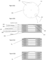
- FIG 2(a) depicts an array of sensors (or sensor stacks) 201 distributed across the surface of a semiconductor wafer probe 101.
- figure 2(a) shows a plan view of a 300 mm wafer probe 101 with nine sensors 201.
- An alignment notch 202 is also shown.
- these sensors 201 are preferably ion energy analysers for measurement of ion energy distribution at the substrate surface of the wafer probe 101.
- Figure 3(a) shows one possible architecture where each sensor 201 of the wafer probe 101 is modularised having its own dedicated power source, signal conditioning circuit, MCU, pressure sensor and wireless transponder.
- the electronic control circuit is centralised and the individual collector currents from each sensing element are multiplexed to a centralised measurement circuit as shown in figure 3(b) .
- the ion energy analyser 201 is of particular interest for measuring the ion energy distribution at the substrate surface during plasma processing.
- the ion energy analyser 201 comprises alternating layers of planar, parallel, conductive metal grids and insulators, the grids being electrically polarised in a systematic way to filter out plasma electrons, separate positive ions based on their energy, suppress secondary electron emission and collect ion current for measurement.
- the plasma facing top surface 203 of the sensor 201 is flush with the substrate surface and made from the same material.
- An array of sampling apertures 204 are formed in this top surface 203, through which plasma species enter the device for analysis.
- the sampling apertures 204 can be sub millimetre in diameter and must provide sufficient open area to deliver adequate charged particle flux for detection.
- a plasma sheath forms adjacent to the surface of the substrate and all other surfaces exposed to the plasma. The voltage applied to the sheath is used to manipulate the ion energy arriving at the substrate surface.
- the presence of the sensor apertures 204 have the potential to inhibit local sheath formation in the vicinity of said apertures.
- Any aperture exposed to the plasma should have dimensions that are smaller than the plasma Debye length ( ⁇ D ) to enable sheath formation above the aperture and thus prevent plasma penetration through the aperture.
- ⁇ 0 is the vacuum permittivity
- kT e is the electron temperature
- n e is the electron density
- e is the electronic charge.
- the Debye length is approximately 40 microns. Therefore, the apertures, typically being on a scale of millimetres, may not meet the sub-Debye length criterion in isolation.
- a first conductive grid (or mesh), referred to as G 0 henceforth, is attached to the underside of the apertures 204 with good electrical connection between both surfaces.
- the grid G 0 is manufactured with sub-Debye length aperture size to guarantee plasma screening and has sufficient open area ratio to transmit sufficient ion flux for detection.
- G 0 can be attached to the plasma facing side of the apertures to achieve the same functionality as illustrated in figure 2(c) .
- the apertures 204 are manufactured directly in the plasma facing surface with sub-Debye length dimensions and in sufficient numbers to maintain adequate ion flux for detection, thus eliminating the need for an independent G 0 .
- This embodiment is illustrated in figure 2(d) .
- G 0 adopts the same potential as the wafer probe outer body, determined by the excitation potential applied to the processing pedestal and the plasma properties. This potential acts as the reference potential for the sensor circuitry and the inter-grid electric field formation.
- a first insulation layer 205 is disposed proximate to G 0 , to provide electrical isolation from other grids e.g., G 1 , G 2 , and G 3 .
- the insulation layer 205 can be made up of one or multiple insulators. Insulators may have an aperture array matching the ion sampling aperture array to allow ions pass through unimpeded. Insulators may alternatively have a single, large diameter aperture with open area spanning the entire aperture array.
- a second grid is disposed proximate to the first insulator 205 with identical or similar geometrical characteristics to G 0 in terms of aperture size and open area ratio.
- G 1 is coupled to a first voltage source and biased negatively with respect to G 0 , thus creating the retarding electric field required to repel the incoming plasma electrons.
- a second insulation layer 206 with identical or similar dimensions to the first insulation layer is disposed proximate to G 1 .
- a third grid, henceforth referred to as G 2 with identical or similar geometry to the other grids is disposed proximate to the second insulation layer.
- G 2 is coupled to a second voltage source and biased with a positive potential sweep relative to G 0 thus creating the electric field required for ion energy discrimination.
- a third insulation layer 207 with identical or similar dimensions to the other insulation layers, is disposed proximate to G 2 .
- a fourth grid, henceforth referred to as G 3 is disposed proximate to the third insulation layer 207.
- G 3 is coupled to a third voltage source and biased negatively with respect to the collector, thus creating the electric field required for suppressing secondary electron emission from the collector.
- a fourth insulation layer 208 with identical or similar dimensions to the other insulation layers is disposed proximate to G 3 .
- An ion collection electrode, the collector, C is disposed proximate to the fourth insulation layer 208.
- the collector is coupled to a fourth voltage source, through a current measurement circuit, and biased negatively with respect to G 0 to establish an attractive electric field to draw ions towards the collector for detection.
- a final insulation layer 209 is disposed between the collector electrode and the back plate of the sensor chassis.
- the grids are typically made from metals such as nickel or stainless steel but any other process compatible conductive material can be used.
- the insulators are typically made from ceramic, mica or other process compatible insulating material.
- the signal conditioning provides a voltage source for each of grids G 1 , G 2 and G 3 as well as the collector described above.
- the voltage provided to G 2 is variable i.e., a voltage sweep is applied to G 2 .
- Generation of a sufficiently high G 2 voltage sweep range to adequately measure the lED found in common plasma processes is important. Many of the plasma processes encountered generate ions with energies ranging from a few tens of eV to a few thousands of eV. This requires the G 2 voltage sweep range to extend from zero volts to a few thousand volts, relative to G 0 , to adequately probe the lED in various industrial processes.
- Figure 4(a) shows the general configuration of a high voltage generating circuit 400, which can be used to generate the required high voltage sweep range.
- This circuit includes two stages which take the low voltage of a battery and generate the required high voltage sweep. Specific details of possible configurations of each stage are described hereinafter with respect to figures 6 and 7 . However, it will be appreciated that each stage is not limited to the details of figures 6 and/or 7.
- the circuit comprises a low voltage supply B1, a high voltage pulse generator 401 (first stage) and a voltage multiplier 402 (second stage).
- the voltage multiplier 402 is also known as a charge pump in the art.
- the high voltage pulse generator 401 provides a high voltage pulse train to the voltage multiplier 402.
- the voltage multiplier 402 uses the pulse train to charge a series of internal capacitors to charge the output to a voltage multiple times the pulse voltage from the pulse generator 401, typically 4 to 5 times.
- the high voltage generating circuit 400 can be included in the signal conditioning circuitry outlined with respect to figures 3(a) and 3(b) . It will also be appreciated that the battery manager circuity (explained in more detail below) shown in figures 3(a) and 3(b) can be provided in circuit 400.
- the battery manager circuit regulates the battery output voltage to a fixed voltage level.
- the low voltage supply may be a single cell LiPo battery with a 3v DC regulator. It should be further appreciated that the arrangement of the high voltage generating circuit and the battery manager can be chosen as appropriate by the person skilled in the art.
- the circuit of figure 4(a) generates the voltage sweep starting at zero and gradually increases to the maximum i.e., an increasing voltage sweep. Ion current is sampled as the sweep increases.
- a rapid ramp up of the voltage and a slow release results in improved battery performance, That is, less power is taken from the battery for each sweep. Therefore, the sensor can be used for a longer period of time before the battery needs to be replaced or recharged.
- the high voltage generating circuit 500 of figure 4(b) is used to quickly ramp the voltage to the maximum level and then slowly sweep it back to zero.
- This circuit is very similar to the circuit of figure 4(a) but some further elements are required.
- a discharge resistor, R1 is added to control the discharge rate, i.e. timing, for the voltage sweep.
- a discharge switch, S1 is also added to discharge V G2 prior to the voltage sweep being applied to V G2 . That is, the switch between the high voltage output to G 2 and the floating ground is used to discharge G 2 immediately before the voltage sweeping process is initiated. Ion current is sampled as the voltage decreases (voltage sweep descending).
- the circuit 500 allows V G2 to be rapidly charged to just over 2kV within 5 milliseconds and V G2 is then allowed to discharge slowly via R1 over a period of up to 1 second.
- the resistor R1 in figure 4(b) is used to set the discharge time for the high voltage.
- the discharge time could be on the order of seconds (or less) and the ion current is sampled at high speed as the voltage discharges. That is, the resistor is in parallel with the voltage multiplier 402 of the high voltage generating circuit.
- the resistance value of the resistor in parallel with the total capacitance to the floating ground of the voltage multiplier determines the rate at which the voltage discharges.
- Ion current collected on the frame of G 2 is returned to the plasma through resistor R1 to sensor chassis ground.
- the ion current reaching the frame of G 2 is a function of the plasma conditions and can span a wide range.
- the G 2 voltage may not discharge fully to 0 V as one would like. Instead, it may plateau at some level, E, above 0 V as shown in figure 5 .
- the plateau voltage E is determined by the ion current flowing through R1.
- the incoming ion current maintains the charge on the pump capacitors of the voltage multiplier 402.
- the voltage cannot discharge further i.e., cannot discharge to 0 V.
- the low energy region of the ion energy distribution would become inaccessible. That is, the ion energy analyser would not be able to sample ion current for G 2 voltage below E.
- the apparatus in accordance with the present teachings employs a two stage voltage scan in order to obtain measurements across the full ion energy distribution.
- the first stage involves taking ion current measurements while voltage applied to the third conductive grid, G 2 , is ascending and the second stage involves taking ion current measurements while the voltage applied to the third conductive grid, G 2 , is descending.
- the current measurements from both stages are then combined to get the complete set of measurements.
- the plasma may be power on and ion current will flow from the third conductive grid, G 2 , through resistor R1 to the sensor ground. This flow will charge the surface of G 2 to some voltage level shown at 'A' in figure 5 .
- the S1 switch is closed to fully discharge the third conductive grid, G 2 , to 0 V. The closing of the switch results in a near instantaneous discharge of the third grid as can be seen from figure 5 .
- switch S1 is returned to the open position and ion current begins to charge G 2 again as shown at 'B' in figure 5 .
- the ion current is measured at high speed during this period, B, as the third gird G 2 is charged by the incoming ions. G 2 settles at plateau level 'E'.
- the resistance value of the resistor in parallel with the total capacitance to the floating ground of the voltage multiplier and the ion current determines the rate at which the first voltage charges.
- the high voltage generating circuit is triggered and the G 2 voltage is quickly boosted/pumped to its maximum level 'C'.
- G 2 discharges through section 'D' back to level 'E' again, for the reason described earlier, and the ion current is measured during the discharge phase (descending voltage sweep).
- the resistance value of the resistor in parallel with the total capacitance to the floating ground of the voltage multiplier and the ion current determines the rate at which the second voltage discharges.
- the high and low energy regions of the ion energy distribution are then fully recovered when the two regions (charging and discharging) are stitched together for plotting.
- the high voltage generating circuits described herein refer to supplying voltage to the third gird, G 2 , of the sensor, the present teachings are not limited to this.
- the high voltage generating circuits described herein can supply voltage to any grid in the gird stack of the sensor.
- the sensor may be provided with only two conductive grids and the voltage from the high voltage generating circuits applied to one of these.
- the voltage sweep is applied to the grid used for ion energy discrimination and this grid can have any position in the stack of grids.
- the grid used for ion energy discrimination and to which the voltage sweep is applied can be considered to be a discriminator grid.
- the low voltage dc source for the high voltage generating circuits may be a low profile solid state battery with dc voltage output in the range of 2.75 to 4.5V.
- a battery manager is used to disconnect the battery when the voltage depletes below a certain threshold. This in turn disconnects power to the main circuit. Power to the main circuit will not be restored until the battery voltage has recharged above the threshold level.
- the battery manager also draws the charge power from the RF antenna that forms part of the receiver in the docking station.
- the battery manager circuit also regulates the battery output voltage to a fixed voltage level which in the exemplary embodiments is 3.2 V.
- each stage of the high voltage generating circuits 400, 500 of figures 4(a) and 4(b) are described hereinafter with respect to figures 6 and 7 .
- the circuits of both figures 6 and 7 can be configured to operate in accordance with the previously described two stage ion current measurement technique.
- Figure 6 shows one configuration for the high voltage generating circuit
- the microcontroller MCU in figures 3(a) and 3(b)
- the microcontroller powered by the battery, is programmed to output a sinusoidal AC voltage which is swept across a range of frequencies.
- the output is coupled to the primary winding of a step-up transformer.
- the number of turns in the secondary winding is chosen to step up the voltage to the maximum level required for a particular frequency applied to the primary winding input.
- the voltage is rectified to generate a direct current (DC) voltage which may be coupled to a voltage multiplier (stage two) to further multiply the voltage to enhance the voltage range as required.
- the DC voltage generated at the output of the secondary winding is frequency dependent.
- the DC voltage at the output of the secondary winding or multiplier is swept across the required voltage range from zero volts to a few thousand volts depending on the transformer turns ratio used.
- the current is sampled at regular voltage intervals in the high voltage sweep using an ADC to build up the current voltage characteristic.
- a four stage voltage multiplier quadrature
- any number of stages can be chosen as appropriate by the person skilled in the art.
- the high voltage generating circuit shown in figure 6 is herein described in more detail.
- this circuit includes a low voltage to high voltage transformer (T1) (first stage) feeding a voltage multiplier (second stage).
- the voltage multiplier is a type of Cockcroft-Walton voltage multiplier circuit consisting of capacitor components C1, C2, C3 and C4 in combination with diode components D1, D2, D3 and D4.
- a Low voltage AC signal is generated on the primary side of T1 using a H-bridge switch.
- the H-bridge or any similar switching topology, is used to allow bipolar current flow through the primary winding of T1 from the single rail power supply.
- the AC signal frequency and amplitude is controlled by the microcontroller.
- the 1:N turns ratio transformer T1 produces a high voltage AC signal on secondary side.
- VG 2 reaches the maximum level of four times the voltage across C2. It is evident that VG 2 can be gradually increased from zero to the maximum by controlling the frequency and amplitude of the AC signal applied to the primary winding of T1.
- the typical increasing voltage ramp saw-tooth or staircase function used to drive the ion energy discrimination in retarding field analysers can be achieved.
- the AC voltage applied to the primary winding of T1 is turned off in order to reset VG 2 to zero in preparation for the next voltage sweep.
- the switch S1 is also closed at this point to help discharge G 2 and the capacitors quickly.
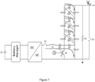
- FIG. 7 illustrates the circuit used to generate the high voltage sweep using this technique.
- the battery delivers a 3V output to the input of a low profile DC-DC converter to increase the voltage to approximately 80V.
- the 80V signal is coupled through a series boost inductor and diode (boost circuit) to a voltage multiplier circuit.
- a field-effect transistor (FET) controlled by a pulse width modulated (PWM) signal is coupled to the system floating ground after the series diode to modulate the 80 V supply and drive the voltage multiplier circuit.
- PWM pulse width modulated
- the voltage multiplier circuit At the input to the voltage multiplier circuit the voltage has been boosted to approximately 250V by the boost circuit, but may be higher as required by the application.
- the voltage multiplier has four stages but can have many more stages to deliver higher and higher voltages.
- Each voltage multiplier stage has the typical design where each stage increases the voltage applied to the input.
- the first capacitor C1 will charge to a maximum level of 500V after a sufficient number of cycles of the PWM signal has taken place.
- the output of C3 will reach 1000 V
- C5 will reach 1500V
- C7 will reach 2000V.
- a series of diodes are configured to prevent the charge storage capacitors from discharging during the PWM off state thus providing the "multiplying" effect desired to generate the high voltage sweep.
- the ion current is sampled at regular voltage intervals in the high voltage sweep using the ADC to build up the current voltage characteristic.
- the configuration of figure 7 was devised to meet more stringent height requirements.
- the battery and battery manager components are the same as in figure 6 .
- the battery manager feeds an off the shelf, low profile, DC-DC converter with integrated voltage doubler to step up the DC voltage level to 80 V.
- the high voltage generating circuit comprises of a boost section followed by a voltage multiplier section.
- the boost section is a typical DC-DC boost converter topology using an inductor L1, MOSFET transistor Q1 (switched on and off with a pulse width modulator), diode D2 and capacitor C1. This allows the circuit charge C1 to voltages greater than 80V, the DC-DC output voltage in the exemplary embodiment therein.
- the multiplier section is very similar to the Cockcroft-Walton type voltage multiplier circuit of figure 6 with capacitor components C2, C3, C4, C5, C6, and C7 and diode components D3, D4, D5, D6, D7 and D8.
- the circuit of figure 7 generates the voltage sweep in a different way compared to the circuit of figure 6 . Instead of a voltage sweep which starts at zero and gradually increases to the maximum, this circuit is used to quickly ramp the voltage to the maximum level and then slowly sweep it back to zero. However, it could also be used to sweep the voltage gradually from zero to maximum voltage.
- any suitable transistor may be chosen e.g., bipolar transistor.
- circuit of figure 6 can be operated in the discontinuous mode described for figure 7 , where the voltage can also be rapidly increased to the maximum before slowly discharging back to zero i.e., the circuit of figure 6 can provide a descending voltage sweep. As is evident to the person skilled in the art, this would require the addition of a discharge resistor, R1, as described in more detail with respect to figures 4(b) and 7 .
- D1 is added to prevent current flowing back to floating ground via L1, from C2, after the energy stored in L1 has depleted.
- a switch S1 is used to connect the boost circuit to the 80V output of the DC-DC converter. S1 remains closed while the VG 2 is charging to the maximum level.
- the switching rate of the MOSFET transistor Q1 is controlled microprocessor output.
- Q1 When Q1 is open, C1 is charged from the DC-DC converter 80 V output and the energised inductor, via D1 and D2. Then C3 is charged by C2 via D4, C5 is charged by C4 via D6 and C7 is charged by C6 via D8.
- Q1 is closed, L1 is energised by current flowing from the DC-DC converter to floating ground via Q1.
- switch S2 is closed to initiate the discharge of VG 2 and slowly decrease it to zero volts.
- Resistor R1 is placed in parallel with S2. The combination of R1 and the capacitors set the VG 2 discharge sweep rate.
- the voltage multiplier (stage 2 of the high voltage generating circuit) of figure 7 has 2 parallel strings of capacitors, (C1, C3, C5 and C7) and (C2, C4 and C6).
- the transistor switch Q1 When the transistor switch Q1 is open, the input to the multiplier is high, and it charges C1, C2 charges C3, C4 charges C5, and C6 charges C7.
- Q1 When Q1 is closed, input is low and C1 charges C2, C3 charges C4, and C5 charges C6.
- the switch Q1 is toggled on and off repeatedly so that all capacitors have a charge voltage equivalent to the input voltage. As a result, the output VG 2 is 4 times the input voltage.
- Using the voltage multiplier directly from the 80V line would give a maximum voltage of about 300V, when efficiency is taken into account.
- the voltage multiplier is preceded by a boost circuit.
- Energy is stored in an inductor L1 and transferred to a capacitor C1, where diode D1 prevents the energy going back to the input via the inductor.
- the input to the boost circuit is 80V, when the transistor is on, the inductor is short to ground, increasing the inductor current and storing energy. When the transistor is off, current will continue to flow through the inductor to capacitor C7 via D8 and D1. The voltage across capacitor C7 will increase as its stored energy increases.
- the input voltage is 80V, the MOSFET transistor shorts both the inductor and voltage multiplier input to ground. The transistor is released after a few microseconds, which induces the current needed to achieve the charge pumping effect to generate the maximum voltage VG 2 .
Landscapes
- Physics & Mathematics (AREA)
- Chemical & Material Sciences (AREA)
- Analytical Chemistry (AREA)
- Engineering & Computer Science (AREA)
- Plasma & Fusion (AREA)
- Spectroscopy & Molecular Physics (AREA)
- Health & Medical Sciences (AREA)
- Life Sciences & Earth Sciences (AREA)
- General Physics & Mathematics (AREA)
- High Energy & Nuclear Physics (AREA)
- Molecular Biology (AREA)
- Plasma Technology (AREA)
- Drying Of Semiconductors (AREA)
- Investigating, Analyzing Materials By Fluorescence Or Luminescence (AREA)
Claims (11)
- Procédé de fonctionnement d'un appareil (101) pour obtenir des mesures de distribution d'énergie ionique dans un système de traitement au plasma comprenant :la fourniture d'un substrat à placer dans le système de traitement au plasma et à exposer au plasma, le substrat ayant un analyseur d'énergie ionique (201) disposé à l'intérieur pour mesurer la distribution d'énergie ionique au niveau de la surface de substrat pendant le traitement au plasma, l'analyseur comprenant une pluralité de grilles conductrices, et une électrode de collecte, chaque grille étant séparée par une couche isolante (205) ;la fourniture d'un circuit générateur de haute tension (400, 500) à l'intérieur du substrat et configuré pour prendre la tension de sortie d'une batterie pour alimenter le circuit générateur de haute tension (400, 500) et appliquer une tension à une première grille de la pluralité de grilles conductrices ;la fourniture d'un commutateur haute tension (S1) configuré pour décharger la première grille vers une masse flottante de l'appareil (101), et une résistance en parallèle avec le commutateur haute tension (S1) ;l'échantillonnage d'un courant ionique pendant une première étape pendant qu'une première tension est chargée sur la première grille à partir du potentiel de masse flottante jusqu'à une tension de plateau ; etl'échantillonnage d'un courant ionique pendant une seconde étape tandis qu'une seconde tension appliquée à la première grille se décharge à travers la résistance à partir d'une tension prédéterminée générée par le circuit générateur de haute tension (400, 500) jusqu'à la tension de plateau.
- Procédé selon la revendication 1, comprenant en outre la fermeture du commutateur (S1) pour décharger la première grille vers la masse flottante avant d'échantillonner le courant ionique pendant la première étape.
- Procédé selon la revendication 1 ou 2, comprenant en outre l'ouverture du commutateur (S1) pour permettre au courant ionique à partir d'un processus au plasma de charger la première grille à la tension de plateau.
- Procédé selon l'une quelconque des revendications 1 à 3, dans lequel la tension de plateau est déterminée par le courant ionique à partir du processus au plasma s'écoulant à travers la résistance.
- Procédé selon l'une quelconque des revendications 1 à 4, dans lequel la première tension est un balayage de tension ascendant et la seconde tension est un balayage de tension descendant.
- Procédé selon l'une quelconque des revendications 1 à 5, dans lequel le circuit haute tension (400, 500) comprend un multiplicateur de tension (402) et la résistance est en parallèle avec le multiplicateur de tension (402).
- Procédé selon la revendication 6, dans lequel la valeur de résistance de la résistance en parallèle avec la capacité totale par rapport à la masse flottante du multiplicateur de tension (402) et au courant ionique détermine la vitesse à laquelle la seconde tension se décharge.
- Procédé selon la revendication 6 ou 7, dans lequel la valeur de résistance de la résistance en parallèle avec la capacité totale par rapport à la masse flottante du multiplicateur de tension (402) et au courant ionique détermine la vitesse à laquelle la première tension se charge.
- Procédé selon l'une quelconque des revendications 1 à 8, comprenant en outre la combinaison du courant ionique échantillonné pendant la première étape avec le courant ionique échantillonné pendant la seconde étape pour obtenir un ensemble complet de mesures sur toute la distribution d'énergie ionique.
- Procédé selon la revendication 9, comprenant en outre le tracé de l'ensemble complet de mesures pour fournir une distribution d'énergie ionique.
- Procédé selon l'une quelconque des revendications 1 à 10, dans lequel la pluralité de grilles conductrices est agencée sous forme d'un empilement de grilles et la première grille est l'une quelconque des grilles de l'empilement, la première grille étant utilisée pour une discrimination d'énergie ionique.
Priority Applications (6)
| Application Number | Priority Date | Filing Date | Title |
|---|---|---|---|
| EP21207043.7A EP4177928B1 (fr) | 2021-11-09 | 2021-11-09 | Méthode de mesure de courant ionique en deux étapes dans un dispositif d'analyse de processus plasma |
| US17/948,465 US12580166B2 (en) | 2021-11-09 | 2022-09-20 | Two stage ion current measurement in a device for analysis of plasma processes |
| TW111136197A TW202320112A (zh) | 2021-11-09 | 2022-09-23 | 電漿製程分析裝置中之兩級離子電流量測 |
| CN202211172028.4A CN116106964A (zh) | 2021-11-09 | 2022-09-26 | 用于分析等离子体处理的装置中的两阶段离子电流测量 |
| JP2022157770A JP2023070637A (ja) | 2021-11-09 | 2022-09-30 | プラズマプロセスを分析するためのデバイスにおける2段階イオン電流測定 |
| KR1020220147214A KR20230067543A (ko) | 2021-11-09 | 2022-11-07 | 플라스마 프로세스의 분석을 위한 장치에서의 2단계 이온 전류 측정 |
Applications Claiming Priority (1)
| Application Number | Priority Date | Filing Date | Title |
|---|---|---|---|
| EP21207043.7A EP4177928B1 (fr) | 2021-11-09 | 2021-11-09 | Méthode de mesure de courant ionique en deux étapes dans un dispositif d'analyse de processus plasma |
Publications (2)
| Publication Number | Publication Date |
|---|---|
| EP4177928A1 EP4177928A1 (fr) | 2023-05-10 |
| EP4177928B1 true EP4177928B1 (fr) | 2024-01-03 |
Family
ID=78592563
Family Applications (1)
| Application Number | Title | Priority Date | Filing Date |
|---|---|---|---|
| EP21207043.7A Active EP4177928B1 (fr) | 2021-11-09 | 2021-11-09 | Méthode de mesure de courant ionique en deux étapes dans un dispositif d'analyse de processus plasma |
Country Status (6)
| Country | Link |
|---|---|
| US (1) | US12580166B2 (fr) |
| EP (1) | EP4177928B1 (fr) |
| JP (1) | JP2023070637A (fr) |
| KR (1) | KR20230067543A (fr) |
| CN (1) | CN116106964A (fr) |
| TW (1) | TW202320112A (fr) |
Families Citing this family (1)
| Publication number | Priority date | Publication date | Assignee | Title |
|---|---|---|---|---|
| CN119601447A (zh) * | 2023-09-11 | 2025-03-11 | 中国科学院微电子研究所 | 用于浸没式等离子体注入设备的离子能量分布测试装置 |
Citations (1)
| Publication number | Priority date | Publication date | Assignee | Title |
|---|---|---|---|---|
| US20050115673A1 (en) * | 2002-03-26 | 2005-06-02 | Seiji Samukawa | On-wafer monitoring system |
Family Cites Families (12)
| Publication number | Priority date | Publication date | Assignee | Title |
|---|---|---|---|---|
| JPS60126832A (ja) * | 1983-12-14 | 1985-07-06 | Hitachi Ltd | ドライエツチング方法および装置 |
| US5451784A (en) * | 1994-10-31 | 1995-09-19 | Applied Materials, Inc. | Composite diagnostic wafer for semiconductor wafer processing systems |
| KR101144449B1 (ko) * | 2003-09-22 | 2012-05-10 | 엠케이에스 인스트루먼츠, 인코포레이티드 | 무선 주파수 플라즈마 프로세싱 내에서 불안정성을 방지하기 위한 장치 및 방법 |
| JP2008166702A (ja) * | 2006-12-06 | 2008-07-17 | Jeol Ltd | 荷電粒子ビーム装置 |
| JP2009111301A (ja) * | 2007-11-01 | 2009-05-21 | Hitachi High-Technologies Corp | プラズマ処理装置 |
| US7875859B2 (en) * | 2008-03-31 | 2011-01-25 | Tokyo Electron Limited | Ion energy analyzer and methods of manufacturing and operating |
| US9287086B2 (en) * | 2010-04-26 | 2016-03-15 | Advanced Energy Industries, Inc. | System, method and apparatus for controlling ion energy distribution |
| US8889021B2 (en) * | 2010-01-21 | 2014-11-18 | Kla-Tencor Corporation | Process condition sensing device and method for plasma chamber |
| US20120283973A1 (en) * | 2011-05-05 | 2012-11-08 | Imec | Plasma probe and method for plasma diagnostics |
| JP5850581B2 (ja) * | 2013-11-29 | 2016-02-03 | 株式会社京三製作所 | プラズマ未着火状態判別装置およびプラズマ未着火判別方法 |
| US11476145B2 (en) * | 2018-11-20 | 2022-10-18 | Applied Materials, Inc. | Automatic ESC bias compensation when using pulsed DC bias |
| EP3968353A1 (fr) * | 2020-09-10 | 2022-03-16 | Impedans Ltd | Appareil pour l'analyse de l'énergie ionique de procédés plasma |
-
2021
- 2021-11-09 EP EP21207043.7A patent/EP4177928B1/fr active Active
-
2022
- 2022-09-20 US US17/948,465 patent/US12580166B2/en active Active
- 2022-09-23 TW TW111136197A patent/TW202320112A/zh unknown
- 2022-09-26 CN CN202211172028.4A patent/CN116106964A/zh active Pending
- 2022-09-30 JP JP2022157770A patent/JP2023070637A/ja active Pending
- 2022-11-07 KR KR1020220147214A patent/KR20230067543A/ko active Pending
Patent Citations (1)
| Publication number | Priority date | Publication date | Assignee | Title |
|---|---|---|---|---|
| US20050115673A1 (en) * | 2002-03-26 | 2005-06-02 | Seiji Samukawa | On-wafer monitoring system |
Also Published As
| Publication number | Publication date |
|---|---|
| US20230143487A1 (en) | 2023-05-11 |
| US12580166B2 (en) | 2026-03-17 |
| CN116106964A (zh) | 2023-05-12 |
| JP2023070637A (ja) | 2023-05-19 |
| EP4177928A1 (fr) | 2023-05-10 |
| KR20230067543A (ko) | 2023-05-16 |
| TW202320112A (zh) | 2023-05-16 |
Similar Documents
| Publication | Publication Date | Title |
|---|---|---|
| JP7743276B2 (ja) | プラズマプロセスのイオンエネルギー分析用の装置 | |
| JP7534528B2 (ja) | 基板処理のためのパルス電圧ブースト | |
| KR102913186B1 (ko) | 이온 전류 보상의 장치 및 방법 | |
| KR20230025486A (ko) | 플라즈마 프로세싱 애플리케이션들을 위한 펄스 전압 소스 | |
| EP3509157B1 (fr) | Batterie secondaire | |
| US12580166B2 (en) | Two stage ion current measurement in a device for analysis of plasma processes | |
| TW202605898A (zh) | 用於電漿製程之離子能量分析之設備 | |
| Biedrzycki et al. | Energy and time distribution of polarization reversal-induced electron emission from triglycine sulphate crystals | |
| Martemianov et al. | Study of a High-voltage Switching Power Supply Parameters |
Legal Events
| Date | Code | Title | Description |
|---|---|---|---|
| PUAI | Public reference made under article 153(3) epc to a published international application that has entered the european phase |
Free format text: ORIGINAL CODE: 0009012 |
|
| STAA | Information on the status of an ep patent application or granted ep patent |
Free format text: STATUS: REQUEST FOR EXAMINATION WAS MADE |
|
| 17P | Request for examination filed |
Effective date: 20220524 |
|
| AK | Designated contracting states |
Kind code of ref document: A1 Designated state(s): AL AT BE BG CH CY CZ DE DK EE ES FI FR GB GR HR HU IE IS IT LI LT LU LV MC MK MT NL NO PL PT RO RS SE SI SK SM TR |
|
| GRAP | Despatch of communication of intention to grant a patent |
Free format text: ORIGINAL CODE: EPIDOSNIGR1 |
|
| STAA | Information on the status of an ep patent application or granted ep patent |
Free format text: STATUS: GRANT OF PATENT IS INTENDED |
|
| INTG | Intention to grant announced |
Effective date: 20230612 |
|
| GRAS | Grant fee paid |
Free format text: ORIGINAL CODE: EPIDOSNIGR3 |
|
| GRAA | (expected) grant |
Free format text: ORIGINAL CODE: 0009210 |
|
| STAA | Information on the status of an ep patent application or granted ep patent |
Free format text: STATUS: THE PATENT HAS BEEN GRANTED |
|
| AK | Designated contracting states |
Kind code of ref document: B1 Designated state(s): AL AT BE BG CH CY CZ DE DK EE ES FI FR GB GR HR HU IE IS IT LI LT LU LV MC MK MT NL NO PL PT RO RS SE SI SK SM TR |
|
| REG | Reference to a national code |
Ref country code: GB Ref legal event code: FG4D |
|
| REG | Reference to a national code |
Ref country code: DE Ref legal event code: R096 Ref document number: 602021008293 Country of ref document: DE |
|
| REG | Reference to a national code |
Ref country code: CH Ref legal event code: EP |
|
| REG | Reference to a national code |
Ref country code: IE Ref legal event code: FG4D |
|
| REG | Reference to a national code |
Ref country code: LT Ref legal event code: MG9D |
|
| PG25 | Lapsed in a contracting state [announced via postgrant information from national office to epo] |
Ref country code: ES Free format text: LAPSE BECAUSE OF FAILURE TO SUBMIT A TRANSLATION OF THE DESCRIPTION OR TO PAY THE FEE WITHIN THE PRESCRIBED TIME-LIMIT Effective date: 20240103 |
|
| PG25 | Lapsed in a contracting state [announced via postgrant information from national office to epo] |
Ref country code: ES Free format text: LAPSE BECAUSE OF FAILURE TO SUBMIT A TRANSLATION OF THE DESCRIPTION OR TO PAY THE FEE WITHIN THE PRESCRIBED TIME-LIMIT Effective date: 20240103 |
|
| REG | Reference to a national code |
Ref country code: NL Ref legal event code: MP Effective date: 20240103 |
|
| REG | Reference to a national code |
Ref country code: AT Ref legal event code: MK05 Ref document number: 1647693 Country of ref document: AT Kind code of ref document: T Effective date: 20240103 |
|
| PG25 | Lapsed in a contracting state [announced via postgrant information from national office to epo] |
Ref country code: NL Free format text: LAPSE BECAUSE OF FAILURE TO SUBMIT A TRANSLATION OF THE DESCRIPTION OR TO PAY THE FEE WITHIN THE PRESCRIBED TIME-LIMIT Effective date: 20240103 |
|
| PG25 | Lapsed in a contracting state [announced via postgrant information from national office to epo] |
Ref country code: NL Free format text: LAPSE BECAUSE OF FAILURE TO SUBMIT A TRANSLATION OF THE DESCRIPTION OR TO PAY THE FEE WITHIN THE PRESCRIBED TIME-LIMIT Effective date: 20240103 |
|
| PG25 | Lapsed in a contracting state [announced via postgrant information from national office to epo] |
Ref country code: IS Free format text: LAPSE BECAUSE OF FAILURE TO SUBMIT A TRANSLATION OF THE DESCRIPTION OR TO PAY THE FEE WITHIN THE PRESCRIBED TIME-LIMIT Effective date: 20240503 |
|
| PG25 | Lapsed in a contracting state [announced via postgrant information from national office to epo] |
Ref country code: LT Free format text: LAPSE BECAUSE OF FAILURE TO SUBMIT A TRANSLATION OF THE DESCRIPTION OR TO PAY THE FEE WITHIN THE PRESCRIBED TIME-LIMIT Effective date: 20240103 |
|
| PG25 | Lapsed in a contracting state [announced via postgrant information from national office to epo] |
Ref country code: GR Free format text: LAPSE BECAUSE OF FAILURE TO SUBMIT A TRANSLATION OF THE DESCRIPTION OR TO PAY THE FEE WITHIN THE PRESCRIBED TIME-LIMIT Effective date: 20240404 |
|
| PG25 | Lapsed in a contracting state [announced via postgrant information from national office to epo] |
Ref country code: HR Free format text: LAPSE BECAUSE OF FAILURE TO SUBMIT A TRANSLATION OF THE DESCRIPTION OR TO PAY THE FEE WITHIN THE PRESCRIBED TIME-LIMIT Effective date: 20240103 Ref country code: RS Free format text: LAPSE BECAUSE OF FAILURE TO SUBMIT A TRANSLATION OF THE DESCRIPTION OR TO PAY THE FEE WITHIN THE PRESCRIBED TIME-LIMIT Effective date: 20240403 |
|
| PG25 | Lapsed in a contracting state [announced via postgrant information from national office to epo] |
Ref country code: CZ Free format text: LAPSE BECAUSE OF FAILURE TO SUBMIT A TRANSLATION OF THE DESCRIPTION OR TO PAY THE FEE WITHIN THE PRESCRIBED TIME-LIMIT Effective date: 20240103 Ref country code: AT Free format text: LAPSE BECAUSE OF FAILURE TO SUBMIT A TRANSLATION OF THE DESCRIPTION OR TO PAY THE FEE WITHIN THE PRESCRIBED TIME-LIMIT Effective date: 20240103 |
|
| PG25 | Lapsed in a contracting state [announced via postgrant information from national office to epo] |
Ref country code: RS Free format text: LAPSE BECAUSE OF FAILURE TO SUBMIT A TRANSLATION OF THE DESCRIPTION OR TO PAY THE FEE WITHIN THE PRESCRIBED TIME-LIMIT Effective date: 20240403 Ref country code: NO Free format text: LAPSE BECAUSE OF FAILURE TO SUBMIT A TRANSLATION OF THE DESCRIPTION OR TO PAY THE FEE WITHIN THE PRESCRIBED TIME-LIMIT Effective date: 20240403 Ref country code: LT Free format text: LAPSE BECAUSE OF FAILURE TO SUBMIT A TRANSLATION OF THE DESCRIPTION OR TO PAY THE FEE WITHIN THE PRESCRIBED TIME-LIMIT Effective date: 20240103 Ref country code: IS Free format text: LAPSE BECAUSE OF FAILURE TO SUBMIT A TRANSLATION OF THE DESCRIPTION OR TO PAY THE FEE WITHIN THE PRESCRIBED TIME-LIMIT Effective date: 20240503 Ref country code: HR Free format text: LAPSE BECAUSE OF FAILURE TO SUBMIT A TRANSLATION OF THE DESCRIPTION OR TO PAY THE FEE WITHIN THE PRESCRIBED TIME-LIMIT Effective date: 20240103 Ref country code: GR Free format text: LAPSE BECAUSE OF FAILURE TO SUBMIT A TRANSLATION OF THE DESCRIPTION OR TO PAY THE FEE WITHIN THE PRESCRIBED TIME-LIMIT Effective date: 20240404 Ref country code: CZ Free format text: LAPSE BECAUSE OF FAILURE TO SUBMIT A TRANSLATION OF THE DESCRIPTION OR TO PAY THE FEE WITHIN THE PRESCRIBED TIME-LIMIT Effective date: 20240103 Ref country code: BG Free format text: LAPSE BECAUSE OF FAILURE TO SUBMIT A TRANSLATION OF THE DESCRIPTION OR TO PAY THE FEE WITHIN THE PRESCRIBED TIME-LIMIT Effective date: 20240103 Ref country code: AT Free format text: LAPSE BECAUSE OF FAILURE TO SUBMIT A TRANSLATION OF THE DESCRIPTION OR TO PAY THE FEE WITHIN THE PRESCRIBED TIME-LIMIT Effective date: 20240103 |
|
| PG25 | Lapsed in a contracting state [announced via postgrant information from national office to epo] |
Ref country code: PT Free format text: LAPSE BECAUSE OF FAILURE TO SUBMIT A TRANSLATION OF THE DESCRIPTION OR TO PAY THE FEE WITHIN THE PRESCRIBED TIME-LIMIT Effective date: 20240503 Ref country code: PL Free format text: LAPSE BECAUSE OF FAILURE TO SUBMIT A TRANSLATION OF THE DESCRIPTION OR TO PAY THE FEE WITHIN THE PRESCRIBED TIME-LIMIT Effective date: 20240103 |
|
| PG25 | Lapsed in a contracting state [announced via postgrant information from national office to epo] |
Ref country code: SE Free format text: LAPSE BECAUSE OF FAILURE TO SUBMIT A TRANSLATION OF THE DESCRIPTION OR TO PAY THE FEE WITHIN THE PRESCRIBED TIME-LIMIT Effective date: 20240103 Ref country code: PT Free format text: LAPSE BECAUSE OF FAILURE TO SUBMIT A TRANSLATION OF THE DESCRIPTION OR TO PAY THE FEE WITHIN THE PRESCRIBED TIME-LIMIT Effective date: 20240503 Ref country code: PL Free format text: LAPSE BECAUSE OF FAILURE TO SUBMIT A TRANSLATION OF THE DESCRIPTION OR TO PAY THE FEE WITHIN THE PRESCRIBED TIME-LIMIT Effective date: 20240103 Ref country code: LV Free format text: LAPSE BECAUSE OF FAILURE TO SUBMIT A TRANSLATION OF THE DESCRIPTION OR TO PAY THE FEE WITHIN THE PRESCRIBED TIME-LIMIT Effective date: 20240103 |
|
| REG | Reference to a national code |
Ref country code: DE Ref legal event code: R097 Ref document number: 602021008293 Country of ref document: DE |
|
| PG25 | Lapsed in a contracting state [announced via postgrant information from national office to epo] |
Ref country code: DK Free format text: LAPSE BECAUSE OF FAILURE TO SUBMIT A TRANSLATION OF THE DESCRIPTION OR TO PAY THE FEE WITHIN THE PRESCRIBED TIME-LIMIT Effective date: 20240103 |
|
| PG25 | Lapsed in a contracting state [announced via postgrant information from national office to epo] |
Ref country code: SM Free format text: LAPSE BECAUSE OF FAILURE TO SUBMIT A TRANSLATION OF THE DESCRIPTION OR TO PAY THE FEE WITHIN THE PRESCRIBED TIME-LIMIT Effective date: 20240103 |
|
| PG25 | Lapsed in a contracting state [announced via postgrant information from national office to epo] |
Ref country code: EE Free format text: LAPSE BECAUSE OF FAILURE TO SUBMIT A TRANSLATION OF THE DESCRIPTION OR TO PAY THE FEE WITHIN THE PRESCRIBED TIME-LIMIT Effective date: 20240103 |
|
| PG25 | Lapsed in a contracting state [announced via postgrant information from national office to epo] |
Ref country code: SK Free format text: LAPSE BECAUSE OF FAILURE TO SUBMIT A TRANSLATION OF THE DESCRIPTION OR TO PAY THE FEE WITHIN THE PRESCRIBED TIME-LIMIT Effective date: 20240103 |
|
| PG25 | Lapsed in a contracting state [announced via postgrant information from national office to epo] |
Ref country code: SM Free format text: LAPSE BECAUSE OF FAILURE TO SUBMIT A TRANSLATION OF THE DESCRIPTION OR TO PAY THE FEE WITHIN THE PRESCRIBED TIME-LIMIT Effective date: 20240103 Ref country code: SK Free format text: LAPSE BECAUSE OF FAILURE TO SUBMIT A TRANSLATION OF THE DESCRIPTION OR TO PAY THE FEE WITHIN THE PRESCRIBED TIME-LIMIT Effective date: 20240103 Ref country code: RO Free format text: LAPSE BECAUSE OF FAILURE TO SUBMIT A TRANSLATION OF THE DESCRIPTION OR TO PAY THE FEE WITHIN THE PRESCRIBED TIME-LIMIT Effective date: 20240103 Ref country code: EE Free format text: LAPSE BECAUSE OF FAILURE TO SUBMIT A TRANSLATION OF THE DESCRIPTION OR TO PAY THE FEE WITHIN THE PRESCRIBED TIME-LIMIT Effective date: 20240103 Ref country code: DK Free format text: LAPSE BECAUSE OF FAILURE TO SUBMIT A TRANSLATION OF THE DESCRIPTION OR TO PAY THE FEE WITHIN THE PRESCRIBED TIME-LIMIT Effective date: 20240103 |
|
| PLBE | No opposition filed within time limit |
Free format text: ORIGINAL CODE: 0009261 |
|
| STAA | Information on the status of an ep patent application or granted ep patent |
Free format text: STATUS: NO OPPOSITION FILED WITHIN TIME LIMIT |
|
| P01 | Opt-out of the competence of the unified patent court (upc) registered |
Free format text: CASE NUMBER: UPC_APP_117901/2023 Effective date: 20230510 |
|
| PG25 | Lapsed in a contracting state [announced via postgrant information from national office to epo] |
Ref country code: IT Free format text: LAPSE BECAUSE OF FAILURE TO SUBMIT A TRANSLATION OF THE DESCRIPTION OR TO PAY THE FEE WITHIN THE PRESCRIBED TIME-LIMIT Effective date: 20240103 |
|
| 26N | No opposition filed |
Effective date: 20241007 |
|
| PG25 | Lapsed in a contracting state [announced via postgrant information from national office to epo] |
Ref country code: IT Free format text: LAPSE BECAUSE OF FAILURE TO SUBMIT A TRANSLATION OF THE DESCRIPTION OR TO PAY THE FEE WITHIN THE PRESCRIBED TIME-LIMIT Effective date: 20240103 |
|
| PG25 | Lapsed in a contracting state [announced via postgrant information from national office to epo] |
Ref country code: SI Free format text: LAPSE BECAUSE OF FAILURE TO SUBMIT A TRANSLATION OF THE DESCRIPTION OR TO PAY THE FEE WITHIN THE PRESCRIBED TIME-LIMIT Effective date: 20240103 |
|
| REG | Reference to a national code |
Ref country code: CH Ref legal event code: PL |
|
| PG25 | Lapsed in a contracting state [announced via postgrant information from national office to epo] |
Ref country code: MC Free format text: LAPSE BECAUSE OF FAILURE TO SUBMIT A TRANSLATION OF THE DESCRIPTION OR TO PAY THE FEE WITHIN THE PRESCRIBED TIME-LIMIT Effective date: 20240103 |
|
| PG25 | Lapsed in a contracting state [announced via postgrant information from national office to epo] |
Ref country code: LU Free format text: LAPSE BECAUSE OF NON-PAYMENT OF DUE FEES Effective date: 20241109 |
|
| REG | Reference to a national code |
Ref country code: CH Ref legal event code: PL |
|
| PG25 | Lapsed in a contracting state [announced via postgrant information from national office to epo] |
Ref country code: CH Free format text: LAPSE BECAUSE OF NON-PAYMENT OF DUE FEES Effective date: 20241130 |
|
| REG | Reference to a national code |
Ref country code: BE Ref legal event code: MM Effective date: 20241130 |
|
| PG25 | Lapsed in a contracting state [announced via postgrant information from national office to epo] |
Ref country code: FI Free format text: LAPSE BECAUSE OF FAILURE TO SUBMIT A TRANSLATION OF THE DESCRIPTION OR TO PAY THE FEE WITHIN THE PRESCRIBED TIME-LIMIT Effective date: 20240103 |
|
| REG | Reference to a national code |
Ref country code: DE Country of ref document: DE Ref country code: DE Ref legal event code: R082 Ref document number: 602021008293 Country of ref document: DE Representative=s name: ZIMMERMANN & PARTNER PATENTANWAELTE MBB, DE |
|
| PG25 | Lapsed in a contracting state [announced via postgrant information from national office to epo] |
Ref country code: BE Free format text: LAPSE BECAUSE OF NON-PAYMENT OF DUE FEES Effective date: 20241130 |
|
| PGFP | Annual fee paid to national office [announced via postgrant information from national office to epo] |
Ref country code: GB Payment date: 20250911 Year of fee payment: 5 |
|
| PG25 | Lapsed in a contracting state [announced via postgrant information from national office to epo] |
Ref country code: IE Free format text: LAPSE BECAUSE OF NON-PAYMENT OF DUE FEES Effective date: 20241109 |
|
| REG | Reference to a national code |
Ref country code: GB Ref legal event code: 732E Free format text: REGISTERED BETWEEN 20251023 AND 20251029 |
|
| REG | Reference to a national code |
Ref country code: DE Ref legal event code: R081 Ref document number: 602021008293 Country of ref document: DE Owner name: APPLIED MATERIALS, INC., SANTA CLARA, US Free format text: FORMER OWNER: IMPEDANS LTD, DUBLIN, IE Ref country code: DE Ref legal event code: R082 Ref document number: 602021008293 Country of ref document: DE Representative=s name: ZIMMERMANN & PARTNER PATENTANWAELTE MBB, DE |
|
| PGFP | Annual fee paid to national office [announced via postgrant information from national office to epo] |
Ref country code: DE Payment date: 20251118 Year of fee payment: 5 |
|
| PGFP | Annual fee paid to national office [announced via postgrant information from national office to epo] |
Ref country code: FR Payment date: 20251125 Year of fee payment: 5 |
|
| PG25 | Lapsed in a contracting state [announced via postgrant information from national office to epo] |
Ref country code: HU Free format text: LAPSE BECAUSE OF FAILURE TO SUBMIT A TRANSLATION OF THE DESCRIPTION OR TO PAY THE FEE WITHIN THE PRESCRIBED TIME-LIMIT; INVALID AB INITIO Effective date: 20211109 |
|
| PG25 | Lapsed in a contracting state [announced via postgrant information from national office to epo] |
Ref country code: CY Free format text: LAPSE BECAUSE OF FAILURE TO SUBMIT A TRANSLATION OF THE DESCRIPTION OR TO PAY THE FEE WITHIN THE PRESCRIBED TIME-LIMIT; INVALID AB INITIO Effective date: 20211109 |