EP4178036A1 - Antenne uwb et dispositif électronique la comprenant - Google Patents
Antenne uwb et dispositif électronique la comprenant Download PDFInfo
- Publication number
- EP4178036A1 EP4178036A1 EP21853152.3A EP21853152A EP4178036A1 EP 4178036 A1 EP4178036 A1 EP 4178036A1 EP 21853152 A EP21853152 A EP 21853152A EP 4178036 A1 EP4178036 A1 EP 4178036A1
- Authority
- EP
- European Patent Office
- Prior art keywords
- patch antenna
- uwb
- antenna
- signal
- transmission line
- Prior art date
- Legal status (The legal status is an assumption and is not a legal conclusion. Google has not performed a legal analysis and makes no representation as to the accuracy of the status listed.)
- Granted
Links
Images













Classifications
-
- H—ELECTRICITY
- H01—ELECTRIC ELEMENTS
- H01Q—ANTENNAS, i.e. RADIO AERIALS
- H01Q5/00—Arrangements for simultaneous operation of antennas on two or more different wavebands, e.g. dual-band or multi-band arrangements
- H01Q5/20—Arrangements for simultaneous operation of antennas on two or more different wavebands, e.g. dual-band or multi-band arrangements characterised by the operating wavebands
- H01Q5/25—Ultra-wideband [UWB] systems, e.g. multiple resonance systems; Pulse systems
-
- H—ELECTRICITY
- H01—ELECTRIC ELEMENTS
- H01Q—ANTENNAS, i.e. RADIO AERIALS
- H01Q21/00—Antenna arrays or systems
- H01Q21/06—Arrays of individually energised antenna units similarly polarised and spaced apart
- H01Q21/061—Two dimensional planar arrays
- H01Q21/065—Patch antenna array
-
- G—PHYSICS
- G01—MEASURING; TESTING
- G01S—RADIO DIRECTION-FINDING; RADIO NAVIGATION; DETERMINING DISTANCE OR VELOCITY BY USE OF RADIO WAVES; LOCATING OR PRESENCE-DETECTING BY USE OF THE REFLECTION OR RERADIATION OF RADIO WAVES; ANALOGOUS ARRANGEMENTS USING OTHER WAVES
- G01S3/00—Direction-finders for determining the direction from which infrasonic, sonic, ultrasonic or electromagnetic waves, or particle emission, not having a directional significance, are being received
- G01S3/02—Direction-finders for determining the direction from which infrasonic, sonic, ultrasonic or electromagnetic waves, or particle emission, not having a directional significance, are being received using radio waves
- G01S3/04—Details
- G01S3/043—Receivers
-
- H—ELECTRICITY
- H01—ELECTRIC ELEMENTS
- H01Q—ANTENNAS, i.e. RADIO AERIALS
- H01Q1/00—Details of, or arrangements associated with, antennas
- H01Q1/12—Supports; Mounting means
- H01Q1/22—Supports; Mounting means by structural association with other equipment or articles
- H01Q1/24—Supports; Mounting means by structural association with other equipment or articles with receiving set
- H01Q1/241—Supports; Mounting means by structural association with other equipment or articles with receiving set used in mobile communications, e.g. GSM
-
- H—ELECTRICITY
- H01—ELECTRIC ELEMENTS
- H01Q—ANTENNAS, i.e. RADIO AERIALS
- H01Q1/00—Details of, or arrangements associated with, antennas
- H01Q1/36—Structural form of radiating elements, e.g. cone, spiral, umbrella; Particular materials used therewith
- H01Q1/38—Structural form of radiating elements, e.g. cone, spiral, umbrella; Particular materials used therewith formed by a conductive layer on an insulating support
-
- H—ELECTRICITY
- H01—ELECTRIC ELEMENTS
- H01Q—ANTENNAS, i.e. RADIO AERIALS
- H01Q1/00—Details of, or arrangements associated with, antennas
- H01Q1/44—Details of, or arrangements associated with, antennas using equipment having another main function to serve additionally as an antenna, e.g. means for giving an antenna an aesthetic aspect
- H01Q1/46—Electric supply lines or communication lines
-
- H—ELECTRICITY
- H01—ELECTRIC ELEMENTS
- H01Q—ANTENNAS, i.e. RADIO AERIALS
- H01Q21/00—Antenna arrays or systems
- H01Q21/24—Combinations of antenna units polarised in different directions for transmitting or receiving circularly and elliptically polarised waves or waves linearly polarised in any direction
-
- H—ELECTRICITY
- H01—ELECTRIC ELEMENTS
- H01Q—ANTENNAS, i.e. RADIO AERIALS
- H01Q3/00—Arrangements for changing or varying the orientation or the shape of the directional pattern of the waves radiated from an antenna or antenna system
- H01Q3/26—Arrangements for changing or varying the orientation or the shape of the directional pattern of the waves radiated from an antenna or antenna system varying the relative phase or relative amplitude of energisation between two or more active radiating elements; varying the distribution of energy across a radiating aperture
- H01Q3/2605—Array of radiating elements provided with a feedback control over the element weights, e.g. adaptive arrays
-
- H—ELECTRICITY
- H01—ELECTRIC ELEMENTS
- H01Q—ANTENNAS, i.e. RADIO AERIALS
- H01Q9/00—Electrically-short antennas having dimensions not more than twice the operating wavelength and consisting of conductive active radiating elements
- H01Q9/04—Resonant antennas
- H01Q9/0407—Substantially flat resonant element parallel to ground plane, e.g. patch antenna
-
- H—ELECTRICITY
- H01—ELECTRIC ELEMENTS
- H01Q—ANTENNAS, i.e. RADIO AERIALS
- H01Q9/00—Electrically-short antennas having dimensions not more than twice the operating wavelength and consisting of conductive active radiating elements
- H01Q9/04—Resonant antennas
- H01Q9/0407—Substantially flat resonant element parallel to ground plane, e.g. patch antenna
- H01Q9/0414—Substantially flat resonant element parallel to ground plane, e.g. patch antenna in a stacked or folded configuration
-
- H—ELECTRICITY
- H01—ELECTRIC ELEMENTS
- H01Q—ANTENNAS, i.e. RADIO AERIALS
- H01Q9/00—Electrically-short antennas having dimensions not more than twice the operating wavelength and consisting of conductive active radiating elements
- H01Q9/04—Resonant antennas
- H01Q9/0407—Substantially flat resonant element parallel to ground plane, e.g. patch antenna
- H01Q9/0428—Substantially flat resonant element parallel to ground plane, e.g. patch antenna radiating a circular polarised wave
-
- G—PHYSICS
- G01—MEASURING; TESTING
- G01S—RADIO DIRECTION-FINDING; RADIO NAVIGATION; DETERMINING DISTANCE OR VELOCITY BY USE OF RADIO WAVES; LOCATING OR PRESENCE-DETECTING BY USE OF THE REFLECTION OR RERADIATION OF RADIO WAVES; ANALOGOUS ARRANGEMENTS USING OTHER WAVES
- G01S3/00—Direction-finders for determining the direction from which infrasonic, sonic, ultrasonic or electromagnetic waves, or particle emission, not having a directional significance, are being received
- G01S3/02—Direction-finders for determining the direction from which infrasonic, sonic, ultrasonic or electromagnetic waves, or particle emission, not having a directional significance, are being received using radio waves
- G01S3/14—Systems for determining direction or deviation from predetermined direction
- G01S3/46—Systems for determining direction or deviation from predetermined direction using antennas spaced apart and measuring phase or time difference between signals therefrom, i.e. path-difference systems
- G01S3/48—Systems for determining direction or deviation from predetermined direction using antennas spaced apart and measuring phase or time difference between signals therefrom, i.e. path-difference systems the waves arriving at the antennas being continuous or intermittent and the phase difference of signals derived therefrom being measured
Definitions
- Various embodiments of the disclosure relate to an electronic device including an ultra-wideband (UWB) antenna.
- UWB ultra-wideband
- An electronic device may perform UWB communication with another electronic device (e.g., a responder) to perform a positioning operation of searching for the location of another electronic device. For example, the electronic device may compute an angle of arrival (AoA) of an RF signal received from another electronic device by using a UWB antenna including at least two patch antennas, and determine the location of another electronic device by using the AoA.
- AoA angle of arrival
- An AoA may include an azimuth angle (e.g., a horizontal angle) and an elevation angle (e.g., a vertical angle), and a UWB antenna may include three patch antennas to measure the azimuth angle and the elevation angle.
- an azimuth angle e.g., a horizontal angle
- an elevation angle e.g., a vertical angle
- a UWB antenna may include three patch antennas to measure the azimuth angle and the elevation angle.
- Each of the patch antennas is formed on a substrate.
- a transmission line for connecting a patch antenna to a UWB communication circuit may be implemented on a flexible printed circuit board (FPCB).
- the FPCB may be bent when patch antennas are assembled in an electronic device, the patch antennas are separated from each other, and thus it may be not easy to arrange the patch antennas in a space inside a housing of the electronic device
- the UWB antenna may be implemented as an FPCB having a multi-layer structure.
- the UWB antenna may include a layer on which patch antennas are formed, a layer on which a transmission line is formed, and a ground layer.
- Such a multi-layer structure may be complex because there are many via processes for electrically connecting the transmission line and the patch antenna. The via processes may cause high costs.
- Various embodiments may provide a UWB antenna structure which can be not only easily disposed in a space inside a housing but also simply manufactured. An electronic device can accurately measure the location of another electronic by performing a positioning operation by using the UWB antenna structure.
- an ultra-wideband (UWB) antenna may include: a dielectric substrate; a first conductive layer disposed on one surface of the dielectric substrate; and a second conductive layer disposed on the other surface of the dielectric substrate.
- the first conductive layer may include a first patch antenna having a structure of receiving a first UWB signal of a first frequency band, in which a polarity direction of an electric field is a vertical linear polarization, and a second UWB signal of a second frequency band, in which a polarity direction of an electric field is a horizontal linear polarization; a second patch antenna which is disposed to be spaced apart from the first patch antenna in a first direction, and has a structure identical to that of the first patch antenna; a third patch antenna which is disposed to be spaced apart from the first patch antenna in a second direction perpendicular to the first direction, and has a structure identical that of the first patch antenna; a first transmission line configured to connect a connector and the first patch antenna; a second
- the second conductive layer may include a ground pattern which overlaps with the first patch antenna, the second patch antenna, the third patch antenna, the first transmission line, the second transmission line, and the third transmission line when facing the second conductive layer in a third direction that is perpendicular to the first direction and the second direction.
- an ultra-wideband (UWB) antenna may include: a dielectric substrate; a first conductive layer disposed on one surface of the dielectric substrate; and a second conductive layer disposed on the other surface of the dielectric substrate.
- the first conductive layer may include: a first patch antenna having a structure of receiving a UWB signal in which a polarity direction of an electric field is a circular polarization; a second patch antenna which is disposed to be spaced apart from the first patch antenna in a first direction while not overlapping with the first patch antenna, and has a structure identical to that of the first patch antenna; a third patch antenna which is disposed to be spaced from the first patch antenna in a second direction perpendicular to the first direction while not overlapping with the first patch antenna, and has a structure identical to that of the first patch antenna; a first transmission line configured to connect a connector and the first patch antenna; a second transmission line configured to connect the connector and the second patch antenna; and a third transmission line configured to connect the connector and the
- the second conductive layer may include a ground pattern which overlaps with the first patch antenna, the second patch antenna, the third patch antenna, the first transmission line, the second transmission line, and the third transmission line when facing the second conductive layer in a third direction perpendicular to the first direction and the second direction.
- an electronic device may include: an ultra-wideband (UWB) antenna; a processor; and a communication circuit configured to: convert a baseband signal received from the processor into an RF signal of a frequency band designated to be used for UWB communication, and output the same to an UWB antenna; and convert an RF signal received from the UWB antenna into a baseband signal, and output the same to the processor.
- the UWB antenna may have a structure of receiving a first UWB signal in which a polarity direction of an electric field is a vertical linear polarization and a second UWB signal in which a polarity direction of an electric field is a horizontal linear polarization.
- the processor may be configured to: while receiving a UWB signal of a first communication channel from an external electronic device through the communication circuit, in case that a signal of the first communication channel received first from the external electronic device is a first signal of the first communication channel, which has a largest signal strength, perform an angle of arrival (AoA) operation by using a main signal of the first communication channel; transmit a message requesting to transmit a UWB signal of a second communication channel, to the external electronic device through the communication circuit in case that the first signal of the first communication channel is not the main signal of the first communication channel; while receiving a UWB signal of the second communication channel from the external electronic device through the communication circuit, in case that a signal of the second communication channel received first from the external electronic device is a main signal of the second communication channel, which has a largest signal strength, perform an AoA operation by using a first signal of the second communication channel; and perform an AoA operation by using the main signal of the first communication channel or the main signal of the second communication channel in case that the first signal of
- Various embodiments of the discourse may provide a UWB antenna which can be easily disposed in an electronic device and relatively simply manufactured. According to various embodiments of the disclosure, costs of an UWB antenna included in an electronic device can be reduced. The electronic device can measure the location of another electronic device by using the UWB antenna.
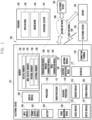
- Fig. 1 is a block diagram illustrating an electronic device 101 in a network environment 100 according to various embodiments.
- the electronic device 101 in the network environment 100 may communicate with an electronic device 102 via a first network 198 (e.g., a short-range wireless communication network), or at least one of an electronic device 104 or a server 108 via a second network 199 (e.g., a long-range wireless communication network).
- the electronic device 101 may communicate with the electronic device 104 via the server 108.
- the electronic device 101 may include a processor 120, memory 130, an input module 150, a sound output module 155, a display module 160, an audio module 170, a sensor module 176, an interface 177, a connecting terminal 178, a haptic module 179, a camera module 180, a power management module 188, a battery 189, a communication module 190, a subscriber identification module(SIM) 196, or an antenna module 197.
- at least one of the components e.g., the connecting terminal 178) may be omitted from the electronic device 101, or one or more other components may be added in the electronic device 101.
- some of the components e.g., the sensor module 176, the camera module 180, or the antenna module 197) may be implemented as a single component (e.g., the display module 160).
- the processor 120 may execute, for example, software (e.g., a program 140) to control at least one other component (e.g., a hardware or software component) of the electronic device 101 coupled with the processor 120, and may perform various data processing or computation. According to one embodiment, as at least part of the data processing or computation, the processor 120 may store a command or data received from another component (e.g., the sensor module 176 or the communication module 190) in volatile memory 132, process the command or the data stored in the volatile memory 132, and store resulting data in non-volatile memory 134.
- software e.g., a program 140
- the processor 120 may store a command or data received from another component (e.g., the sensor module 176 or the communication module 190) in volatile memory 132, process the command or the data stored in the volatile memory 132, and store resulting data in non-volatile memory 134.
- the processor 120 may include a main processor 121 (e.g., a central processing unit (CPU) or an application processor (AP)), or an auxiliary processor 123 (e.g., a graphics processing unit (GPU), a neural processing unit (NPU), an image signal processor (ISP), a sensor hub processor, or a communication processor (CP)) that is operable independently from, or in conjunction with, the main processor 121.
- a main processor 121 e.g., a central processing unit (CPU) or an application processor (AP)
- auxiliary processor 123 e.g., a graphics processing unit (GPU), a neural processing unit (NPU), an image signal processor (ISP), a sensor hub processor, or a communication processor (CP)
- the main processor 121 may be adapted to consume less power than the main processor 121, or to be specific to a specified function.
- the auxiliary processor 123 may be implemented as separate from, or as part of the main processor 121.
- the auxiliary processor 123 may control at least some of functions or states related to at least one component (e.g., the display module 160, the sensor module 176, or the communication module 190) among the components of the electronic device 101, instead of the main processor 121 while the main processor 121 is in an inactive (e.g., sleep) state, or together with the main processor 121 while the main processor 121 is in an active state (e.g., executing an application).
- the auxiliary processor 123 e.g., an image signal processor or a communication processor
- the auxiliary processor 123 may include a hardware structure specified for artificial intelligence model processing.
- An artificial intelligence model may be generated by machine learning. Such learning may be performed, e.g., by the electronic device 101 where the artificial intelligence is performed or via a separate server (e.g., the server 108). Learning algorithms may include, but are not limited to, e.g., supervised learning, unsupervised learning, semi-supervised learning, or reinforcement learning.
- the artificial intelligence model may include a plurality of artificial neural network layers.
- the artificial neural network may be a deep neural network (DNN), a convolutional neural network (CNN), a recurrent neural network (RNN), a restricted boltzmann machine (RBM), a deep belief network (DBN), a bidirectional recurrent deep neural network (BRDNN), deep Q-network or a combination of two or more thereof but is not limited thereto.
- the artificial intelligence model may, additionally or alternatively, include a software structure other than the hardware structure.
- the memory 130 may store various data used by at least one component (e.g., the processor 120 or the sensor module 176) of the electronic device 101.
- the various data may include, for example, software (e.g., the program 140) and input data or output data for a command related thererto.
- the memory 130 may include the volatile memory 132 or the non-volatile memory 134.
- the program 140 may be stored in the memory 130 as software, and may include, for example, an operating system (OS) 142, middleware 144, or an application 146.
- OS operating system
- middleware middleware
- application application
- the input module 150 may receive a command or data to be used by another component (e.g., the processor 120) of the electronic device 101, from the outside (e.g., a user) of the electronic device 101.
- the input module 150 may include, for example, a microphone, a mouse, a keyboard, a key (e.g., a button), or a digital pen (e.g., a stylus pen).
- the sound output module 155 may output sound signals to the outside of the electronic device 101.
- the sound output module 155 may include, for example, a speaker or a receiver.
- the speaker may be used for general purposes, such as playing multimedia or playing record.
- the receiver may be used for receiving incoming calls. According to an embodiment, the receiver may be implemented as separate from, or as part of the speaker.
- the display module 160 may visually provide information to the outside (e.g., a user) of the electronic device 101.
- the display module 160 may include, for example, a display, a hologram device, or a projector and control circuitry to control a corresponding one of the display, hologram device, and projector.
- the display module 160 may include a touch sensor adapted to detect a touch, or a pressure sensor adapted to measure the intensity of force incurred by the touch.
- the audio module 170 may convert a sound into an electrical signal and vice versa. According to an embodiment, the audio module 170 may obtain the sound via the input module 150, or output the sound via the sound output module 155 or a headphone of an external electronic device (e.g., an electronic device 102) directly (e.g., wiredly) or wirelessly coupled with the electronic device 101.
- an external electronic device e.g., an electronic device 102
- directly e.g., wiredly
- wirelessly e.g., wirelessly
- the sensor module 176 may detect an operational state (e.g., power or temperature) of the electronic device 101 or an environmental state (e.g., a state of a user) external to the electronic device 101, and then generate an electrical signal or data value corresponding to the detected state.
- the sensor module 176 may include, for example, a gesture sensor, a gyro sensor, an atmospheric pressure sensor, a magnetic sensor, an acceleration sensor, a grip sensor, a proximity sensor, a color sensor, an infrared (IR) sensor, a biometric sensor, a temperature sensor, a humidity sensor, or an illuminance sensor.
- the interface 177 may support one or more specified protocols to be used for the electronic device 101 to be coupled with the external electronic device (e.g., the electronic device 102) directly (e.g., wiredly) or wirelessly.
- the interface 177 may include, for example, a high definition multimedia interface (HDMI), a universal serial bus (USB) interface, a secure digital (SD) card interface, or an audio interface.
- HDMI high definition multimedia interface
- USB universal serial bus
- SD secure digital
- a connecting terminal 178 may include a connector via which the electronic device 101 may be physically connected with the external electronic device (e.g., the electronic device 102).
- the connecting terminal 178 may include, for example, a HDMI connector, a USB connector, a SD card connector, or an audio connector (e.g., a headphone connector).
- the haptic module 179 may convert an electrical signal into a mechanical stimulus (e.g., a vibration or a movement) or electrical stimulus which may be recognized by a user via his tactile sensation or kinesthetic sensation.
- the haptic module 179 may include, for example, a motor, a piezoelectric element, or an electric stimulator.
- the camera module 180 may capture a still image or moving images.
- the camera module 180 may include one or more lenses, image sensors, image signal processors, or flashes.
- the power management module 188 may manage power supplied to the electronic device 101.
- the power management module 188 may be implemented as at least part of, for example, a power management integrated circuit (PMIC).
- PMIC power management integrated circuit
- the battery 189 may supply power to at least one component of the electronic device 101.
- the battery 189 may include, for example, a primary cell which is not rechargeable, a secondary cell which is rechargeable, or a fuel cell.
- the communication module 190 may support establishing a direct (e.g., wired) communication channel or a wireless communication channel between the electronic device 101 and the external electronic device (e.g., the electronic device 102, the electronic device 104, or the server 108) and performing communication via the established communication channel.
- the communication module 190 may include one or more communication processors that are operable independently from the processor 120 (e.g., the application processor (AP)) and supports a direct (e.g., wired) communication or a wireless communication.
- AP application processor
- the communication module 190 may include a wireless communication module 192 (e.g., a cellular communication module, a short-range wireless communication module, or a global navigation satellite system (GNSS) communication module) or a wired communication module 194 (e.g., a local area network (LAN) communication module or a power line communication (PLC) module).
- a wireless communication module 192 e.g., a cellular communication module, a short-range wireless communication module, or a global navigation satellite system (GNSS) communication module
- GNSS global navigation satellite system
- wired communication module 194 e.g., a local area network (LAN) communication module or a power line communication (PLC) module.
- LAN local area network
- PLC power line communication
- a corresponding one of these communication modules may communicate with the external electronic device via the first network 198 (e.g., a short-range communication network, such as BluetoothTM, wireless-fidelity (Wi-Fi) direct, or infrared data association (IrDA)) or the second network 199 (e.g., a long-range communication network, such as a legacy cellular network, a 5G network, a next-generation communication network, the Internet, or a computer network (e.g., LAN or wide area network (WAN)).
- first network 198 e.g., a short-range communication network, such as BluetoothTM, wireless-fidelity (Wi-Fi) direct, or infrared data association (IrDA)
- the second network 199 e.g., a long-range communication network, such as a legacy cellular network, a 5G network, a next-generation communication network, the Internet, or a computer network (e.g., LAN or wide area network (WAN)).
- the wireless communication module 192 may identify and authenticate the electronic device 101 in a communication network, such as the first network 198 or the second network 199, using subscriber information (e.g., international mobile subscriber identity (IMSI)) stored in the subscriber identification module 196.
- subscriber information e.g., international mobile subscriber identity (IMSI)
- the wireless communication module 192 may support a 5G network, after a 4G network, and next-generation communication technology, e.g., new radio (NR) access technology.
- the NR access technology may support enhanced mobile broadband (eMBB), massive machine type communications (mMTC), or ultra-reliable and low-latency communications (URLLC).
- eMBB enhanced mobile broadband
- mMTC massive machine type communications
- URLLC ultra-reliable and low-latency communications
- the wireless communication module 192 may support a high-frequency band (e.g., the mmWave band) to achieve, e.g., a high data transmission rate.
- the wireless communication module 192 may support various technologies for securing performance on a high-frequency band, such as, e.g., beamforming, massive multiple-input and multiple-output (massive MIMO), full dimensional MIMO (FD-MIMO), array antenna, analog beam-forming, or large scale antenna.
- the wireless communication module 192 may support various requirements specified in the electronic device 101, an external electronic device (e.g., the electronic device 104), or a network system (e.g., the second network 199).
- the wireless communication module 192 may support a peak data rate (e.g., 20Gbps or more) for implementing eMBB, loss coverage (e.g., 164dB or less) for implementing mMTC, or U-plane latency (e.g., 0.5ms or less for each of downlink (DL) and uplink (LTL), or a round trip of 1ms or less) for implementing URLLC.
- a peak data rate e.g., 20Gbps or more
- loss coverage e.g., 164dB or less
- U-plane latency e.g., 0.5ms or less for each of downlink (DL) and uplink (LTL), or a round trip of 1ms or less
- the antenna module 197 may transmit or receive a signal or power to or from the outside (e.g., the external electronic device) of the electronic device 101.
- the antenna module 197 may include an antenna including a radiating element composed of a conductive material or a conductive pattern formed in or on a substrate (e.g., a printed circuit board (PCB)).
- the antenna module 197 may include a plurality of antennas (e.g., array antennas). In such a case, at least one antenna appropriate for a communication scheme used in the communication network, such as the first network 198 or the second network 199, may be selected, for example, by the communication module 190 (e.g., the wireless communication module 192) from the plurality of antennas.
- the signal or the power may then be transmitted or received between the communication module 190 and the external electronic device via the selected at least one antenna.
- another component e.g., a radio frequency integrated circuit (RFIC)
- RFIC radio frequency integrated circuit
- the antenna module 197 may form a mmWave antenna module.
- the mmWave antenna module may include a printed circuit board, a RFIC disposed on a first surface (e.g., the bottom surface) of the printed circuit board, or adjacent to the first surface and capable of supporting a designated high-frequency band (e.g., the mmWave band), and a plurality of antennas (e.g., array antennas) disposed on a second surface (e.g., the top or a side surface) of the printed circuit board, or adjacent to the second surface and capable of transmitting or receiving signals of the designated high-frequency band.
- a RFIC disposed on a first surface (e.g., the bottom surface) of the printed circuit board, or adjacent to the first surface and capable of supporting a designated high-frequency band (e.g., the mmWave band)
- a plurality of antennas e.g., array antennas
- At least some of the above-described components may be coupled mutually and communicate signals (e.g., commands or data) therebetween via an inter-peripheral communication scheme (e.g., a bus, general purpose input and output (GPIO), serial peripheral interface (SPI), or mobile industry processor interface (MIPI)).
- an inter-peripheral communication scheme e.g., a bus, general purpose input and output (GPIO), serial peripheral interface (SPI), or mobile industry processor interface (MIPI)
- commands or data may be transmitted or received between the electronic device 101 and the external electronic device 104 via the server 108 coupled with the second network 199.
- Each of the electronic devices 102 or 104 may be a device of a same type as, or a different type, from the electronic device 101.
- all or some of operations to be executed at the electronic device 101 may be executed at one or more of the external electronic devices 102, 104, or 108. For example, if the electronic device 101 should perform a function or a service automatically, or in response to a request from a user or another device, the electronic device 101, instead of, or in addition to, executing the function or the service, may request the one or more external electronic devices to perform at least part of the function or the service.
- the one or more external electronic devices receiving the request may perform the at least part of the function or the service requested, or an additional function or an additional service related to the request, and transfer an outcome of the performing to the electronic device 101.
- the electronic device 101 may provide the outcome, with or without further processing of the outcome, as at least part of a reply to the request.
- a cloud computing, distributed computing, mobile edge computing (MEC), or client-server computing technology may be used, for example.
- the electronic device 101 may provide ultra low-latency services using, e.g., distributed computing or mobile edge computing.
- the external electronic device 104 may include an internet-of-things (IoT) device.
- the server 108 may be an intelligent server using machine learning and/or a neural network.
- the external electronic device 104 or the server 108 may be included in the second network 199.
- the electronic device 101 may be applied to intelligent services (e.g., smart home, smart city, smart car, or healthcare) based on 5G communication technology or IoT-related technology.
- the electronic device may be one of various types of electronic devices.
- the electronic devices may include, for example, a portable communication device (e.g., a smartphone), a computer device, a portable multimedia device, a portable medical device, a camera, a wearable device, or a home appliance. According to an embodiment of the disclosure, the electronic devices are not limited to those described above.
- each of such phrases as “A or B,” “at least one of A and B,” “at least one of A or B,” “A, B, or C,” “at least one of A, B, and C,” and “at least one of A, B, or C,” may include any one of, or all possible combinations of the items enumerated together in a corresponding one of the phrases.
- such terms as “1st” and “2nd,” or “first” and “second” may be used to simply distinguish a corresponding component from another, and does not limit the components in other aspect (e.g., importance or order).
- an element e.g., a first element
- the element may be coupled with the other element directly (e.g., wiredly), wirelessly, or via a third element.
- module may include a unit implemented in hardware, software, or firmware, and may interchangeably be used with other terms, for example, “logic,” “logic block,” “part,” or “circuitry”.
- a module may be a single integral component, or a minimum unit or part thereof, adapted to perform one or more functions.
- the module may be implemented in a form of an application-specific integrated circuit (ASIC).
- ASIC application-specific integrated circuit
- Various embodiments as set forth herein may be implemented as software (e.g., the program 140) including one or more instructions that are stored in a storage medium (e.g., internal memory 136 or external memory 138) that is readable by a machine (e.g., the electronic device 101).
- a processor e.g., the processor 120
- the machine e.g., the electronic device 101
- the one or more instructions may include a code generated by a complier or a code executable by an interpreter.
- the machine-readable storage medium may be provided in the form of a non-transitory storage medium.
- non-transitory simply means that the storage medium is a tangible device, and does not include a signal (e.g., an electromagnetic wave), but this term does not differentiate between where data is semi-permanently stored in the storage medium and where the data is temporarily stored in the storage medium.
- a method may be included and provided in a computer program product.
- the computer program product may be traded as a product between a seller and a buyer.
- the computer program product may be distributed in the form of a machine-readable storage medium (e.g., compact disc read only memory (CD-ROM)), or be distributed (e.g., downloaded or uploaded) online via an application store (e.g., PlayStoreTM), or between two user devices (e.g., smart phones) directly. If distributed online, at least part of the computer program product may be temporarily generated or at least temporarily stored in the machine-readable storage medium, such as memory of the manufacturer's server, a server of the application store, or a relay server.
- CD-ROM compact disc read only memory
- an application store e.g., PlayStoreTM
- two user devices e.g., smart phones
- each component e.g., a module or a program of the above-described components may include a single entity or multiple entities, and some of the multiple entities may be separately disposed in different components. According to various embodiments, one or more of the above-described components may be omitted, or one or more other components may be added. Alternatively or additionally, a plurality of components (e.g., modules or programs) may be integrated into a single component. In such a case, according to various embodiments, the integrated component may still perform one or more functions of each of the plurality of components in the same or similar manner as they are performed by a corresponding one of the plurality of components before the integration.
- operations performed by the module, the program, or another component may be carried out sequentially, in parallel, repeatedly, or heuristically, or one or more of the operations may be executed in a different order or omitted, or one or more other operations may be added.
- FIG. 2 is a block diagram 200 illustrating a wireless communication module 192 and an antenna module 197 of an electronic device 101 according to various embodiments.
- the wireless communication module 192 may include a Bluetooth communication circuit 210 and/or a UWB communication circuit 220.
- the antenna module 197 may include a Bluetooth antenna 250 connected to the Bluetooth communication circuit 210, and/or a UWB antenna 220 connected to the UWB communication circuit 220.
- At least one function of the Bluetooth communication circuit 210 and the UWB communication circuit 220 may be controlled by a processor 120 (e.g., an application processor and/or a communication processor).
- a processor 120 e.g., an application processor and/or a communication processor.
- the Bluetooth communication circuit 210 may support establishment of a Bluetooth communication channel (or session) corresponding to a frequency band designated to be used for Bluetooth (e.g., Bluetooth low energy (BLE)), among bands to be used for wireless communication with an external electronic device (e.g., the external electronic device 102 of FIG. 1 ).
- the Bluetooth communication circuit 210 may support Bluetooth communication with the external electronic device through the Bluetooth communication channel.
- the Bluetooth communication circuit 210 may convert a baseband signal generated by the processor 120 (e.g., the application processor and/or the communication processor) and received from the processor 120 into an RF signal of a Bluetooth band, and transmit the converted signal to the outside through the Bluetooth antenna 250.
- the Bluetooth communication circuit 210 may acquire an RF signal of a Bluetooth band (e.g., about 2.4 GHz) through the Bluetooth antenna 250, and convert the acquired RF signal into a baseband (e.g., a few MHz or lower) signal to transmit the converted signal to the processor 120
- a Bluetooth band e.g., about 2.4 GHz
- a baseband e.g., a few MHz or lower
- the UWB communication circuit 220 may support establishment of a UWB communication channel (or session) corresponding to a frequency band (e.g., about 3.1 to 10.6 GHz) designated to be used for UWB communication, among bands to be used for wireless communication with an external electronic device (e.g., the external electronic device 102 of FIG. 1 ).
- the UWB communication circuit 220 may support UWB communication with the external electronic device through the UWB communication channel.
- the UWB communication circuit 220 may convert a baseband signal generated by the processor 120 (e.g., the application processor and/or the communication processor) and received from the processor 120 into an RF signal of a UWB band so as to transmit the same to the outside through the UWB antenna 260.
- the UWB communication circuit 220 may acquire an RF signal of a UWB band through the UWB antenna 260, and convert the acquired RF signal into a baseband signal to transmit the converted signal to the processor 120.
- the wireless communication module 192 may further include a filter (e.g., a UWB band pass filter) for filtering out an RF signal of the UWB band from an RF signal received from the UWB antenna 260 and transferring the same to the UWB communication circuit 220.
- the UWB antenna 260 may include multiple antennas.
- the UWB antenna 260 may include an RF signal transmission or reception first antenna or an RF signal reception second antenna and/or third antenna.
- Bluetooth may be utilized as a trigger for activating UWB communication.
- BLE has relatively lower accuracy in positioning compared to other short-distance communication technologies (e.g., UWB technology), but has low consumption power and has a long recognition distance (e.g., a distance within which the existence of a surrounding external electronic device 102 can be recognized), and thus BLE may be used for triggering activation of positioning communication.
- the processor 120 may receive a signal (e.g., an advertising or broadcasting packet) for connection with the external electronic device 102 to the external electronic device 102 through the Bluetooth communication circuit 210.
- the external electronic device 102 may transmit a signal, as an advertiser (or a broadcaster), and the electronic device 101 may periodically scan a signal, as an observer.
- the processor 120 may determine to activate UWB-employed positioning communication.
- the processor 120 may establish a UWB communication channel (e.g., a second frequency band (e.g., ch5, an about 6.5 GHz, or about 6.25 to 6.75 GHz) or a first frequency (e.g., ch9, about 8 GHz band, or about 7.75 to 8.25 GHz)) with the external electronic device 102 by using the UWB communication circuit 220.
- a UWB communication channel e.g., a second frequency band (e.g., ch5, an about 6.5 GHz, or about 6.25 to 6.75 GHz) or a first frequency (e.g., ch9, about 8 GHz band, or about 7.75 to 8.25 GHz)
- the processor 120 may convert the state of the UWB communication circuit 220 into an enabled state, based on the determination, establish a UWB communication channel with the external electronic device 102 by using the UWB communication circuit 220, and perform positioning communication with the external electronic device 101 through the established UWB communication channel.
- the processor 120 may establish a BLE communication channel with the external electronic device 102 by using the Bluetooth communication circuit 210.
- the processor 120 may determine to active the UWB-employed positioning communication, based on the strength of the signal received from the external electronic device 102 through the established BLE communication channel (e.g., when the strength has a value greater than a designated threshold value, or the strength of the signal gets stronger). According to the determination, the processor 120 may establish a UWB communication channel with the external electronic device 102 by using the UWB communication circuit 220, and perform positioning communication with the external electronic device 101 through the established UWB communication channel.
- a communication technology e.g., Wi-Fi
- Wi-Fi Wi-Fi
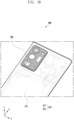
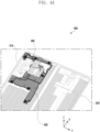
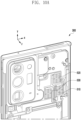
- FIGS. 3A and 3B illustrate disposition of a UWB antenna in a portable electronic device 300 (e.g., the electronic device 101 of FIG. 1 ) having a bar-shaped housing structure according to an embodiment.
- a surface on which a display (e.g., the display module 160 of FIG. 1 ) of the portable electronic device 300 may be defined as a front surface, a surface opposite to the front surface may be defined as a rear surface of the portable electronic device 300, and a surface surrounding a space between the front surface and the rear surface may be defined as a side surface of the portable electronic device 300.
- FIG. 3A is a view illustrating a portable electronic device 300, the rear cover of which is removed, and FIG. 3B illustrates a portable electronic device 300 to which the rear cover thereof is coupled.
- a portable electronic device 300 may include a housing 310, a camera cover 320, a UWB antenna 330, and/or a support member 340.
- the housing 310 may include a front cover (not shown), a rear cover 311, and/or a side frame 312.
- the UWB antenna 330 and the support member 340 may be arranged inside the housing 310.
- the camera cover 320 may decorate, as a cover of a camera module (e.g., the camera module 180) disposed inside the housing 310, the camera module, and may be implemented as metal or polymer.
- the UWB antenna 330 (e.g., the UWB antenna 260 of FIG. 2 ) may be disposed inside the housing 310 while not overlapping with the camera module when facing the rear surface.
- the UWB antenna 330 may be electrically disconnected from the camera cover 320, and may be disposed between the rear cover 311 and the support member 340.
- the support member 340 may be disposed between the UWB antenna 330 and a substrate (e.g., printed circuit board (PCB)) (not shown).
- the UWB antenna 330 may be disposed on the support member 340.
- the support member 340 may be implemented as, for example, metal (e.g., SUS) or polymer.
- the support member 340 may holes 350 formed to be fixed inside the housing 310 by using fixing members (e.g., screws).
- the support member 340 may be electrically connected to the side frame 312 (e.g., a metal body) through screws.
- the UWB antenna 330 may be electrically connected to a UWB communication circuit (e.g., the UWB communication circuit 220 of FIG. 2 ) through a signal line formed on the substrate.
- the portable electronic device may have a foldable housing which is divided into two housings with reference to a folding axis.
- a first part of display e.g., a flexible display
- a second part of the display may be disposed on a second housing.
- the foldable housing may be implemented in an in-folding scheme in which the first part and the second part face each other when the portable electronic device is folded.
- the foldable housing may be implemented in an out-folding scheme in which the first part and the second part face are oriented opposite to each other when the portable electronic device is folded.
- a surface on which the first part and the second part of the display are arranged may be defined as a front surface of the portable electronic device, a surface opposite to the front surface may be defined as a rear surface of the portable electronic device, and a surface surrounding a space between the front surface and the rear surface may be defined as a side surface of the portable electronic device.
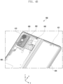
- FIGS. 4A and 4B illustrate disposition of a UWB antenna in a portable electronic device 400 having an in-folding scheme foldable housing structure according to an embodiment.
- the portable electronic device 400 may include a foldable housing 410 and 420 may include a camera cover 430, a UWB antenna 440, and/or a support member 450.
- the foldable housing may include a first housing 410 and a second housing 420.
- the first housing 410 may include a first rear cover (not shown) forming a part of a rear surface of the portable electronic device 400.
- the second housing 420 may include a second rear cover 421 forming another part of the rear surface of the portable electronic device 400.
- the UWB antenna 440 and/or the support member 450 may be arranged inside the first housing 410.
- the camera cover 430 may decorate, as a cover of a camera module received inside the first housing 410, the camera module, and may be implemented as metal or polymer.
- the UWB antenna 440 (e.g., the UWB antenna 260 of FIG. 2 ) may be disposed inside the first housing 410 while not overlapping with a camera module (e.g., the camera module 180 of FIG. 1 ) when facing the rear surface.
- the UWB antenna 440 may be electrically disconnected from the camera cover 430, and may be disposed between a first rear cover and the support member 450.
- the support member 450 may be disposed between the UWB antenna 440 and a substrate (e.g., a PCB) (not shown) disposed inside the first housing 410.
- the support member may be coupled to the UWB antenna 440, and may be implemented as an injection molding.
- the UWB antenna 440 may be electrically connected to a UWB communication circuit (e.g., the UWB communication circuit 220 of FIG. 2 ) through a signal line formed on the substrate.
- an antenna other than the UWB antenna 440 may be disposed inside the first housing 410.
- the portable electronic device 400 may further include a second display disposed inside the second housing 420 and exposed through the second rear cover 421, in addition to a first display exposed through a front surface.
- FIG. 5 illustrates a side surface of a UWB antenna 500 having a laminating structure according to various embodiments.
- a UWB antenna 500 e.g., the UWB antenna 260 of FIG. 2
- the first conductive layer 510 may be formed on one surface of a dielectric substrate (or a dielectric layer) 530
- the second conductive layer 520 may be formed on the other surface of the dielectric substrate 530.
- the first conductive layer 510 may include patch antennas and a transmission line (or a feeding line) for connecting each of the patch antennas to a UWB communication circuit (e.g., the UWB communication circuit 220 of FIG. 2 ).
- the second conductive layer 520 may form a common ground for the patch antennas.
- the patch antennas and the ground may operate as a resonator for transmitting an RF signal of a specific frequency band (e.g., a second frequency band (e.g., ch5 or an about 6.5 GHz band) or a first frequency band (e.g., ch9 or an about 8 GHz band)) to the outside and receiving an RF signal of the specific frequency band.
- a specific frequency band e.g., a second frequency band (e.g., ch5 or an about 6.5 GHz band) or a first frequency band (e.g., ch9 or an about 8 GHz band)
- the first conductive layer 510 may include a first copper layer 511 and/or a first plating layer (e.g., copper plating) 512 plated with the first copper layer.
- the second conductive layer 520 may include a second copper layer 521 and a second plating layer (e.g., copper plating) 522 plated with the second copper layer.
- an insulation material such as polymer may be disposed on the first conductive layer 510 or the second conductive layer 520.
- the dielectric substrate 530 may be implemented so that the UWB antenna 500 transmits or receive an RF signal of a specific frequency band.
- the dielectric substrate 530 may include a first modified polyimide (MPI) 531, a second MPI 532, a third MPI 533, a first bonding sheet 534, and/or a second bonding sheet 535.
- the first copper layer 511 and the first MPI 531 are main materials of an FPCB, and may form a first flexible copper clad laminate (FCCL) 501.
- FCCL flexible copper clad laminate
- the second copper 521 and the second MPI 532 may form a second FCCL 502.
- the first bonding sheet 534 may be disposed between the first MPI 531 and the third MPU 533 to bond the first MPI 531 and the third MPI 533.
- the second bonding sheet 535 may be disposed between the second MPI 532 and the third MPI 533 to bond the second MPI 532 and the third MPI 533.
- the third MPI 533 may be disposed between the first bonding sheet 534 and the second bonding sheet 535.
- the third MPI 533 may be added to the dielectric substrate 530, as a complementary material for complementing the thickness of the dielectric substrate 530.
- the third MPI 533 and at least one of the first bonding sheet 534 and the second bonding sheet 535 may be omitted from elements of the dielectric substrate 530.
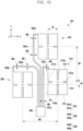
- FIG. 6A illustrates a surface of a first conductive layer 601 of a UWB antenna according to an embodiment
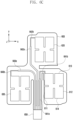
- FIG. 6B illustrates a surface of a second conductive layer 602 disposed under the first conductive layer 601
- FIG. 6C is a perspective view illustrating a UWB antenna on which the first conductive layer 601 and the second conductive layer 602 are arranged.
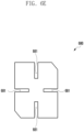
- FIG. 6D , 6E , and 6F illustrate various embodiments of a patch antenna included in a UWB antenna.
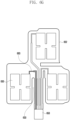
- FIGS. 6G and 6H illustrate the position of a feeding point of each patch antenna of a first conductive layer 601.
- a first conductive layer 601 may include a first patch antenna 610, a second patch antenna 620, a third patch antenna 630, a first transmission line 641, a second transmission line 642, and/or a third transmission line 643.
- one (e.g., a first patch antenna 610) of the patch antennas 610, 620, and 630 may be used as an antenna for UWB signal transmission or reception, and the other two may be used as antennas for UWB signal reception.
- the first patch antenna 610 and a second patch antenna 620 may be arranged in a first direction (y-axis direction) while not overlapping with each other when viewed facing a rear surface (XY plane), so that the angle (e.g., an elevation angle of AoA) in the y-axis direction can be measured.
- the second patch antenna 620 may be disposed to be spaced apart from the first patch antenna 610 in the first direction while not overlapping with the first patch antenna.
- the second patch antenna 620 may have substantially the same shape and size as the first patch antenna 610.
- the center of the first patch antenna 610 may be spaced apart from the center of the second patch antenna 620 by an interval (dx) in the x-axis direction.
- the center of the second patch antenna 620 may be spaced apart from the center of the first patch antenna by an interval (W1) in the y-axis direction.
- the first patch antenna 610 and a third patch antenna 630 may be aligned in a second direction (x-axis direction) substantially perpendicular to the first direction while not overlapping with each other when viewed facing a rear surface (XY plane), so that the angle (e.g., an azimuth angle of AoA) in the x-axis direction can be measured.
- the third patch antenna 630 may be disposed to be spaced from the first patch antenna 610 in a third direction (-x-axis direction) while not overlapping with the first patch antenna.
- the third patch antenna 630 may have substantially the same shape and size as the first patch antenna 610.
- the center of the third patch antenna 630 may be spaced apart from the center of the first patch antenna 610 by an interval (dy) in the y-axis direction.
- the center of the third patch antenna 630 may be spaced apart from the center of the first patch antenna 610 by an interval (W2) in the x-axis direction.
- the interval (W1), the interval (W2), the interval (dx), or the interval (dy) may be determined based on a resonance frequency band of the UWB antenna, and may be determined not to exceed a half-wave length in consideration of characteristics of the AoA.
- the interval (W1) may be implemented to be about 13 to 20 mm (e.g., about 14 mm)
- the interval (dx) may be implemented to be about 3.6 mm
- the interval (W2) may be implemented to be about 13 to 20 mm (e.g., about 13 mm)
- the interval (dy) may be implemented to be about 1.0 mm.
- multiple slits may be formed at the patch antennas 610, 620, and 630 so that simultaneous resonance is performed in a dual frequency band, and a vertical linear polarization in which a polarity direction of an electric field is a y-axis direction and a traveling direction of an RF signal is a z-axis direction and a horizontal linear polarization in which a polarity direction of an electric field is an x-axis direction and a traveling direction of an RF signal is a z-axis direction are transmitted and/or received.
- the patch antennas 610, 620, and 630 may be symmetric when viewed with reference to the x-axis and y-axis directions.
- each of the patch antennas 610, 620, and 630 may be a rectangle (or a square).
- the first patch antenna 610 may include a first side (or a left side) 611 extending in the y-axis direction, a second side (or a right side) 612 in parallel to the first side 611, a third side (or a top side) 613 extending in the x-axis direction, and a fourth side (or a bottom side) 614 in parallel to the third side.
- a first slit 611a may be formed in a straight line from the center of the first side 611 towards the second side 612 so as to be perpendicular to the first side 611.
- a second slit 612a may be formed in a straight line from the center of the second side 612 towards the first side 611 so as to be perpendicular to the second side 612.
- a third slit 613a may be formed in a straight line from the center of the third side 613 towards the fourth side 614 so as to be perpendicular to the third side 613.
- a fourth slit 614a may be formed in a straight line from the center of the fourth side 614 towards the third side 613 so as to be perpendicular to the fourth side 614.
- a vertical linear polarization of a first frequency band may be transmitted or received by the lengths of electric emission currents of the first side 611, the first slit 611a formed on the first side 611, the second side 612, and the second slit 612a formed on the second side 612.
- a horizontal linear polarization of a second frequency band may be transmitted or received by the lengths of electric emission currents of the third side 613, the third slit 613a formed on the third side 613, the fourth side 614, and the fourth slit 614a formed on the fourth side 614.
- a slit having substantially the same shape as that of the first patch antenna 610 may be also formed at each of the second patch antenna 620 and the third patch antenna 630.
- slits may be also formed at substantially the same position as the first patch antenna 610.
- the lengths of the sides and the slits of the first patch antenna 610, the second patch antenna 620, or the third patch antenna 630 may implemented according to the resonance frequency band.
- the lengths of the first side 611, the second side 612, the first slit 611a, and the second slit 612a of the first patch antenna 610 may be implemented according to a first frequency band (e.g., ch9 or an about 8 GHz band), and the lengths of the third side 613, the fourth side 614, the third slit 613a, and the fourth slit 614a may be implemented according to a second frequency band (e.g., ch5 or an about 6.5 GHz band).
- a first frequency band e.g., ch9 or an about 8 GHz band
- a second frequency band e.g., ch5 or an about 6.5 GHz band
- FIG. 6D illustrates that the lengths of a first side 671, a second side 672, a first slit 671a, and a second slit 672a are implemented according to a second frequency band (e.g., ch5 or an about 6.5 GHz band), and the lengths of a third side 673, a fourth side 674, a third slit 673a, and a fourth slit 674a are implemented according to a first frequency band (e.g., ch9 or an about 8 GHz band).
- a second frequency band e.g., ch5 or an about 6.5 GHz band
- a first frequency band e.g., ch9 or an about 8 GHz band
- reception efficiency of the reception antenna may increase.
- reception efficiency of the reception antenna may decrease.
- a patch antenna implemented to receive a circular polarization may have comparatively low reception efficiency compared to a patch antenna implemented to receive a linear polarization, but when the antenna receives not only the circular polarization but also a vertical linear polarization and a horizontal linear polarization, the reception efficiency thereof may increase compared to the patch antenna implemented to receive the linear polarization.
- a patch antenna implemented to receive a liner polarization has lower reception efficiency than a case of receiving a linear polarization having the same polarity direction, but when the patch antenna receives a circular polarization, the reception efficiency may increase compared to a case of receiving a linear polarization having a different polarity direction.
- a patch antenna may be implemented so that resonance is performed in a single frequency band and a circular polarization is transmitted (or received).
- a patch antenna 680 may have the same overall shape as the first patch antenna 610, and may have a structure in which triangles at a right upper corner and a left lower corner are cut off with reference to the currently illustrated drawing so that a right-hand circular polarization (RHCP) is transmitted or received.
- the shapes of slits 681 formed at the patch antenna 680 may be formed based on a frequency (e.g., a first frequency band (e.g., ch9 or an about 8 GHz band)) supported by the patch antenna 680. Referring to FIG.
- a patch antenna 690 may have the same overall shape as the first patch antenna 610, and may have a structure in which triangles at a right lower corner and a left upper corner are cut off with reference to the currently illustrated drawing so that a left-hand circular polarization (LHCP) is transmitted or received.
- the shapes of slits 691 formed at the patch antenna 690 may be formed based on a frequency (e.g., a first frequency band (e.g., ch9 or an about 8 GHz band)) supported by the patch antenna 690.
- a second conductive layer 602 (e.g., the second conductive layer 320 of FIG. 3 ) according to an embodiment may include a ground pattern 603.
- the ground pattern 603 may be disposed on a substrate (e.g., the dielectric substrate 530 of FIG. 5 ) to overlap with the first conductive layer 601 when viewed facing a rear surface (XY plane).
- the patch antennas 610, 620, and 630 or the transmission lines 641, 642, and 643 included in the first conductive layer 601 may overlap with the ground pattern 603.
- the patch antennas 610, 620, and 630 or the transmission lines 641, 642, and 643 included in the first conductive layer 601 disposed to overlap with the ground pattern 603 may hidden by the ground pattern 603.
- the area of the ground pattern 603 may be greater than those of the patch antennas 610, 620, and 630 or the transmission lines 641, 642, and 643.
- the ground pattern 603 may be formed of one metal plate, as a common ground for the patch antennas 610, 620, and 630, and accordingly, may have a comparatively rigid property. Such a rigid property may cause contact failure between the substrate and a connector 650 when an impact is given to an electronic device from the outside, for example.
- the substrate may have a UWB communication circuit disposed thereon, or may be electrically connected to the UWB communication circuit.
- a part of the ground pattern 603, which overlaps with the connector 650 when viewed in the +z-axis direction may be flexibly implemented.
- a part of the ground pattern 603, which overlaps with the connector 650 may have a different composition ratio of a conductive material from that of a part not overlapping with the connector 650.
- slits 631 when viewed in the z-axis direction, may be formed not to overlap with the transmission lines 641, 642, and 643.
- a slit 632 when viewed from the z-axis direction, may be formed along the y-axis direction so as to be positioned between the first transmission line 641 and the first patch antenna 610 and not to overlap with the first transmission line 641 and the first patch antenna 610.
- a slit 633 may be formed along the y-axis direction so as to be positioned between the third transmission line 643 and the third patch antenna 630 and not to overlap with the third transmission line 643 and the third patch antenna 630.
- a slit for uniformity of a radiation pattern may be formed on the ground pattern 603.
- the uniformity may be defined as a technical feature which causes left and right radiation patterns to have symmetry with reference to a designated direction (e.g., y-axis direction).
- a slit 634 may be formed along the x-axis direction at the edge of the ground pattern 603 so as to be positioned between the first patch antenna 610 and the second patch antenna 620 and not to overlap with the first patch antenna 610 and the second patch antenna 620.
- the locations of feeding points of the patch antennas 610, 620, and 630 connected to transmission lines are corners (or vertices) of the respective patch antennas.
- all the patch antennas 610, 620, and 630 may have substantially the same feeding point at the left upper corner with reference to the currently illustrated drawing.
- a feeding point may be positioned at a corner causing a shortest signal path to be formed between the connector 650 and the patch antenna, among four corners of the patch antenna.
- the length of the transmission line may change.
- a third transmission line 663 shorter than the third transmission line 643 of FIG. 6C may be formed on the first conductive layer 601.
- a third transmission line (not shown) shorter than the third transmission line 663 of FIG. 6G may be formed on the first conductive layer 601.
- a second transmission line 662 shorter than the second transmission line 642 of FIG. 6C may be formed on the first conductive layer 601.
- the shorter the length of the transmission line a loss of the UWB signal in the transmission line may become comparatively small, and accordingly, radiation efficiency of a patch antenna can be enhanced.
- the first conductive layer 601 may be selectively implemented through the change of the length of the transmission line, and AoA calculation may be applied through calibration of even a phase difference according to the change of the length of the transmission line.
- the transmission lines 641, 642, and 643 may extend from the connector 650 to the corner of each of the patch antennas by passing between the first patch antenna 610 and the third patch antenna 630 while not overlapping with one another when viewed facing a rear surface (XY plane).
- the transmission lines 641, 642, and 643 may include first parts 641a, 642a, and 643a each having a first width (W3), and second parts 641b, 642b, and 643b each having a second width (W4).
- the first width (W3) may be implemented so that the first parts 641a, 642a, and 643a have, for example, characteristic impedance of 50 ohms.
- the width of each of the first parts 641a, 642a, and 643a may be implemented to be about 0.5 mm.
- the second parts 641b, 642b, and 643b may function as a transformer (or a trance) for impedance conversion for matching impedance of each of the patch antennas 610, 620, and 630 and characteristic impedance of each of the first parts 641a, 642a, and 643a.
- the second width (W4) may be implemented to be narrower (e.g., about 0.15 mm) than the first width (W3), and the length of each of the second parts 641b, 642b, and 643b may be implemented to be, for example, about 5 mm.
- the length of the width (e.g., the second width (W4)) of each of the second parts 641b, 642b, and 643b may be adjusted for impedance matching between the corresponding patch antennas and the first parts 641a, 642a, and 643a.
- the connector 650 may be electrically connected to a UWB communication circuit.
- the connector 650 may be electrically connected to a UWB communication circuit disposed on a substrate electrically connected to the connector 650.
- FIGS. 7A , 7B , and 7C illustrate a first conductive layer and a second conductive layer of a UWB antenna according to various embodiments.
- patch antennas 711, 712, and 713 may be arranged in a reversed-L shape on a first conductive layer (e.g., the first conductive layer 510 of FIG. 5 ) as shown in FIG. 7A .
- a second patch antenna 712 may be disposed in the y-axis direction of a first patch antenna 711
- a third patch antenna 713 may be disposed in the -x-axis direction of the first patch antenna 711.
- a connector 714 may be disposed in the -y-axis direction of the first patch antenna 711 and the third patch antenna 713.
- Transmission lines 715, 716, and 717 may be formed on the first conductive layer like the patch antennas 711, 712, and 713.
- the transmission lines 715, 716, and 717 may be connected to feeding points at substantially the same positions of the corresponding patch antennas 711, 712, and 713, respectively.
- the first transmission line 715 may extend from the connector 714 to the left upper corner of the first patch antenna 711 by passing between the first patch antenna 711 and the third patch antenna 713.
- the second transmission line 716 may extend from the connector 714 to the left upper corner of the second patch antenna 712 by passing between the first patch antenna 711 and the third patch antenna 713.
- the third transmission line 717 may extend from the connector 714 to the left upper corner of the third patch antenna 713 by passing between the first patch antenna 711 and the third patch antenna 713.
- a second conductive layer may be positioned under the first conductive layer in the -z-axis direction.
- the second conductive layer (e.g., the second conductive layer 520 of FIG. 5 ) may include a common ground pattern 702 (e.g., the ground pattern 603 of FIG. 6B ) for the patch antennas 711, 712, and 713.
- the ground pattern may be disposed to overlap with both the patch antennas 711, 712, and 713 and the transmission lines 715, 716, and 717.
- the patch antennas 711, 712, and 713 and the transmission lines 715, 716, and 717 fall outside the ground pattern 702.
- a slit 721 may be formed at the edge of the ground pattern 702 positioned between the first transmission line 715 and the first patch antenna 711 along an extension direction (y-axis direction) of the first transmission line 715.
- a slit 722 may be formed at the edge of the ground pattern 702 positioned between the third transmission line 717 and the third patch antenna 713 along an extension direction (y-axis direction) of the third transmission line 717.
- a slit 723 may be formed at the edge of the ground pattern 702 positioned between the first patch antenna 711 and the second patch antenna 712 along the x-axis direction.
- the second transmission line 726 may extend from the connector 714 to the right lower corner of the second patch antenna 712 by passing between the first patch antenna 711 and the third patch antenna 713. Accordingly, the second transmission line 726 may be shortened compared to the second transmission line 716 of FIG. 7A . A part 731 through which the transmission line 716 passes in FIG. 7A in the ground pattern 702 may be removed from the ground pattern 702 by the shortened length of the transmission line.
- the third transmission line 727 may extend from the connector 714 to the right upper corner of the third patch antenna 713 by passing between the first patch antenna 711 and the third patch antenna 713.
- the third transmission line 727 may be shortened compared to the third transmission 717 of FIG. 7A .
- a part 732 through which the third transmission line 717 of FIG. 7A passes in the second conductive layer may be removed from the ground pattern 702 by the shortened length of the transmission line.
- the ground pattern 702 may be formed to be physically separated as a first metal plate 751, a second metal plate 752, and a third metal plate 753.
- the first metal plate 751 may be disposed to overlap with the first patch antenna 711 and the first transmission line 715
- the second metal plate 752 may be disposed to overlap with the second patch antenna 712 and the second transmission line 726
- the third metal plate 753 may be disposed to overlap with the third patch antenna 713 and the third transmission line 727.
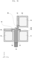
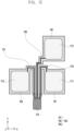
- FIG. 8A illustrates a horizontal linear polarization in a patch antenna according to an embodiment
- FIG. 8B illustrates a vertical linear polarization in the patch antenna of FIG. 8A
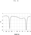
- FIG. 8C illustrates characteristics of dual resonance in the patch antenna of FIG. 8A .
- a resonance frequency may be determined by a horizontal length 810 and a vertical length 820.
- Dual resonance may be implemented in the patch antenna 800 by slits positioned at the edge.
- a first slit 811a may be formed at a first side 811 and a second slit 812a may be formed at a second side 812 so that the patch antenna 800 resonates in a first frequency band (e.g., ch9 or an about 8 GHz band).
- a third slit 813a may be formed at a third side 813 and a fourth slit 814a may be formed at a fourth side 814 so that the patch antenna 800 resonates in a second frequency band (e.g., ch5 or an about 6.5 GHz band).
- a second frequency band e.g., ch5 or an about 6.5 GHz band.
- the third slit 813a and the fourth slit 814a formed in the vertical direction may form a surface current path 830 corresponding the second frequency band.
- the patch antenna 800 may transmit and/or receive a horizontal linear polarization of the second frequency band, in which a polarity direction 840 of an electric field is a horizontal direction (x-axis direction) and a traveling direction is the z-axis direction.
- the first slit 811a and the second slit 812a formed in the horizontal direction may form a surface current path 850 corresponding to the first frequency band.
- the patch antenna 800 may transmit and/or receive a vertical linear polarization of the first frequency band, in which a polarity direction 860 of an electric field is a vertical direction (y-axis direction) and a traveling direction is a z-axis direction.
- the lengths of the first slit 811a and the second slit 812a may be implemented to cause the patch antenna 800 to transmit and/or receive a vertical linear polarization of a second frequency band (e.g., ch5 or an about 6.5 GHz band), and the lengths of the third slit 813a and the fourth slit 814a may be implemented to cause the patch antenna 800 to transmit and/or receive a horizontal polarization of a first frequency band (e.g., ch9 or an about 8 GHz band).
- the lengths of the first slit 811a and the second slit 812a may be shorter than the lengths illustrated in FIG. 8A
- the lengths of the third slit 813a and the fourth slit 814a may be longer than the lengths illustrated in FIG. 8A .
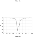
- FIG. 9A illustrates a resonance frequency of the patch antenna 680 of FIG. 6E
- FIG. 9B is a graph indicating an axial ratio of a circular polarization in the patch antenna 680 of FIG. 6E
- the patch antenna 680 may be implemented to resonate in, for example, a first frequency band (e.g., ch9 or an about 8 GHz band).
- the axial ratio may mean a ratio of the polarity of an electric field in the x-axis direction to the polarity of an electric field in the y-axis direction.
- FIG. 9B it may be identified that a polarization having the smallest axial ratio (for example, a polarization closest to a circle) in the first frequency band in which the center frequency thereof is about 8 GHz occurs in the patch antenna 680.
- the lengths of the slits 681 are implemented differently, and thus the resonance frequency of the patch antenna 680 may be, for example, a second frequency band.
- FIGS. 10A and 10B illustrate a radiation pattern when the posture of the portable electronic device 300 of FIG. 3A is a vertical mode (or a portrait mode)
- FIGS. 10C and 10D illustrate a radiation pattern when the posture of the portable electronic device 300 of FIG. 3A is a horizontal mode (or a landscape mode).
- the first patch antenna 610 and the third patch antenna 630 may be aligned in the direction substantially parallel to the x axis, and the first patch antenna 610 and the second patch antennas 620 may be aligned in the direction substantially parallel to the y axis. Accordingly, when the posture of the portable electronic device 300 is the portrait mode, the first patch antenna 610 and the third patch antenna 630 may be used to measure an angle (an azimuth angle) in the x-axis direction of a UWB signal received in the UWB antenna.
- the first patch antenna 610 and the second patch antenna 620 may be used to measure an angle (an elevation angle) in the y-axis direction of a UWB signal received in the UWB antenna.
- a processor e.g., the processor 120 of FIG. 1
- the processor may calculate a phase difference between two signals by using a difference between a reception time of the first signal and a reception time of a third signal received from the third antenna 630, and compute the azimuth angle by using the phase difference and the distance (e.g., "interval (W2)" of FIG. 6A ) between two patch antennas 610 and 630.
- W2 interval
- a common ground pattern of the patch antennas 610, 620, and 630 may be implemented to have an asymmetric structure rather than as structure (e.g., a square) in which right and left sides and/or top and bottom sides are symmetric to each other. Accordingly, the UWB signal of the UWB antenna may be emitted in an asymmetric shape 1010 when viewed in the z-axis direction on the XY plane. In addition, although not shown in FIG. 10B , a null pattern in which no UWB signal is emitted may be generated at a specific angle. As the ground pattern 603 of FIG.
- the UWB signal of the UWB antenna may be emitted, when viewed in the z-axis direction on the XY plane, in a more symmetric shape 1020 than that in a case where the ground pattern has no slit 634 formed thereat.
- the AoA operation can be more comparatively accurate.
- the first patch antenna 610 and the second patch antenna 620 may be aligned in the direction substantially parallel to the x axis
- the first patch antenna 610 and the third patch antennas 630 may be aligned in the direction substantially parallel to the y axis.
- a common ground pattern of the patch antennas 610, 620, and 630 may be implemented to have an asymmetric structure. Accordingly, the UWB signal of the UWB antenna may be emitted in an asymmetric shape 1030 when viewed in the z-axis direction on the XY plane. As the ground pattern 603 of FIG.
- the UWB signal of the UWB antenna may be emitted in a symmetric shape 1040 when viewed in the z-axis direction on the XY plane.
- FIG. 11 illustrates operations 1100 of a processor for positioning according to an embodiment.
- the operations 1100 may be executed by a processor 120 of an electronic device (e.g., the electronic device 101 of FIG. 1 ) operating as an initiator searching for an external electronic device (e.g., the electronic device 102 of FIG. 1 ) (responder).
- a memory e.g., the memory 130 of FIG. 1
- a UWB antenna having a structure e.g., the first conductive layer 601 of FIG.
- the processor 120 may perform the operations 1100 by using a UWB signal received from the UWB antenna through a UWB communication circuit (e.g., the UWB communication circuit 220 of FIG. 2 ).
- the first frequency band may be one of ch5 (e.g., an about 6.5 GHz band) and ch9 (e.g., an about 8 GHz band)
- the second frequency band may be the other of ch9 (e.g., an about 8 GHz band) and ch5 (e.g., an about 6.5 GHz band).
- the first frequency band and the second frequency band are not limited thereto, and may partially overlap, or may be changed to another bandwidth.
- the processor 120 may transmit, to an external electronic device through a UWB communication circuit, a first request message requesting transmission of a signal for positioning of the external electronic device.
- the external electronic device may transmit a UWB signal of an agreed UWB communication channel, for example, a first frequency band.
- the processor 120 may determine whether a signal received first is a main signal of a second frequency band.
- the main signal may mean a signal, the strength (e.g., RSSI) of which is the largest, among received signals of a corresponding channel.
- the first signal arrived at the electronic device is referred to as a line of sight (LOS) signal, and may mean a signal directly arriving at the electronic device without being reflected by a metal object of the external electronic device.
- a next arriving signal is referred to as a not line of sight (NLOS) signal, and may mean a signal arriving at the electronic device after being reflected by a metal object of the external electronic device.
- NLOS not line of sight
- the processor 120 may perform, in operation 1130, an AoA operation by using the LOS signal of the first frequency band.
- the processor 120 may perform operation 1140.
- the LOS signal may not be the main signal.
- the NLOS signal received later may be reflected by the metal object, and the polarization direction thereof may be changed to be closer to the polarization direction of the reception antenna. Accordingly, the NLOS signal may be the main signal.
- the processor 120 may transmit, to the external electronic device through the UWB communication circuit, a second request message requesting transmission of a UWB signal of the second frequency band.
- the external electronic device may transmit a UWB signal of the second frequency band.
- the processor 120 may determine whether the LOS signal received first is a main signal.
- the processor 120 may perform, in operation 1160, an AoA operation by using the LOS signal of the second frequency band.
- the processor 120 may perform operation 1170.
- the processor 120 may compare a signal strength difference (hereinafter, referred to as a first difference value) between the LOS signal of the first frequency band and the main signal of the first frequency band with a signal strength difference (hereinafter, referred to as a second difference value) between the LOS signal of the second frequency band and the main signal of the second frequency band. As a result of the comparison, when the first difference value is greater than the second difference value, the processor 120 may perform the AoA operation by using the main signal of the first frequency band. As a result of the comparison, when the second difference value is greater than the first difference value, the processor 120 may perform, in operation 1180, the AoA operation by using the main signal of the second frequency band.
- a signal strength difference hereinafter, referred to as a first difference value
- a second difference value signal strength difference
- an ultra-wideband (UWB) antenna may include: a dielectric substrate; a first conductive layer disposed on one surface of the dielectric substrate; and a second conductive layer disposed on the other surface of the dielectric substrate.
- the first conductive layer may include: a first patch antenna having a structure of receiving a first UWB signal of a first frequency band, in which a polarity direction of an electric field is a vertical linear polarization, and a second UWB signal of a second frequency band, in which a polarity direction of an electric field is a horizontal linear polarization; a second patch antenna which is disposed to be spaced apart from the first patch antenna in a first direction (e.g., the y-axis direction in FIG.
- a third patch antenna which is disposed to be spaced apart from the first patch antenna in a second direction (e.g., the x-axis direction in FIG. 6A ) perpendicular to the first direction, and has a structure identical that of the first patch antenna; a first transmission line configured to connect a connector and the first patch antenna; a second transmission line configured to connect the connector and the second patch antenna; and a third transmission line configured to connect the connector and the third patch antenna.
- the second conductive layer may include a ground pattern which overlaps with the first patch antenna, the second patch antenna, the third patch antenna, the first transmission line, the second transmission line, and the third transmission line when facing the second conductive layer in a third direction that is perpendicular to the first direction and the second direction.
- a first slit (e.g., 634 of FIG. 6B ) may be formed on the second conductive layer, wherein the first slit is inwardly formed at an edge of a part positioned between the first patch antenna and the second patch antenna when facing the second conductive layer in the third direction.
- the first transmission line, the second transmission line, and the third transmission line may be formed on an upper surface of the dielectric subtract while not overlapping with one another, wherein the first transmission line extends from the connector to the first patch antenna by passing between the first patch antenna and the third patch antenna.
- the second transmission line may extend from the connector to the second patch antenna by passing between the first patch antenna and the third patch antenna.
- the third transmission line may extend from the connector to the third patch antenna by passing between the first patch antenna and the third patch antenna.
- a second slit and a third slit may be formed on the second conductive layer, wherein the second slit (e.g., 631 of FIG. 6B ) is formed between the first transmission line and the second transmission line and between the second transmission line and the third transmission line.
- the third slit e.g., 632 and 633 of FIG. 6B ) may be formed between the third patch antenna and the third transmission line and between the first patch antenna and the first transmission line.
- Each of the first patch antenna, the second patch antenna, and the third patch antenna may be a quadrangle having a first side and a second side extending in parallel to the first direction, and having a third side and a fourth side extending in parallel to the second direction.
- a first slit is formed towards an inside of the quadrangle at the first side in parallel to the second direction and a second slit is formed towards an inside of the quadrangle at the second side in parallel to the second direction, so that the first UWB signal can be received in the UWB antenna.
- a third slit is formed towards an inside of the quadrangle at the third side in parallel to the first direction and a fourth slit is formed towards an inside of the quadrangle at the fourth side in parallel to the first direction, so that the second UWB signal can be received in the UWB antenna.
- the lengths of the first slit and the second slit may be implemented so that the UWB antenna resonates in one of UWB communication channels 5 and 9.
- the lengths of the third slit and the fourth slit may be implemented so that the UWB antenna resonates in the other of UWB communication channels 5 and 9.
- the channel 5 may be about 6.25 to 6.75 GHz
- the channel 9 may be about 7.75 to 8.25 GHz.
- a feeding point may be formed at a corner, for example, a left upper corner of the quadrangle.
- a feeding point may be formed at a corner causing a shortest signal path from the connector to be formed, among four corners of the quadrangle.
- an ultra-wideband (UWB) antenna may include: a dielectric substrate; a first conductive layer disposed on one surface of the dielectric substrate; and a second conductive layer disposed on the other surface of the dielectric substrate.
- the first conductive layer may include: a first patch antenna having a structure of receiving a UWB signal in which a polarity direction of an electric field is a circular polarization; a second patch antenna which is disposed to be spaced apart from the first patch antenna in a first direction (e.g., the y-axis direction in FIG.
- a third patch antenna which is disposed to be spaced from the first patch antenna in a second direction (e.g., the x-axis direction in FIG. 6A ) perpendicular to the first direction while not overlapping with the first patch antenna, and has a structure identical to that of the first patch antenna; a first transmission line configured to connect a connector and the first patch antenna; a second transmission line configured to connect the connector and the second patch antenna; and a third transmission line configured to connect the connector and the third patch antenna.
- the second conductive layer may include a ground pattern which overlaps with the first patch antenna, the second patch antenna, the third patch antenna, the first transmission line, the second transmission line, and the third transmission line when facing the second conductive layer in a third direction perpendicular to the first direction and the second direction.
- Each of the first patch antenna, the second patch antenna, and the third patch antenna may have a structure in which triangles at a first corner and a second corner positioned diagonal to the first corner are cut off from a quadrangle including a first side and a second side extending in parallel to the first direction and a third side and a fourth side extending in parallel to the second direction.
- a first slit may be formed towards an inside of the quadrangle at the first side in parallel to the second direction.
- a second slit may be formed towards an inside of the quadrangle at the second side in parallel to the second direction.
- a third slit may be formed towards an inside of the quadrangle at the third side in parallel to the first direction.
- a fourth slit may be formed towards an inside of the quadrangle at the fourth side in parallel to the first direction.
- the lengths of the first slit, the second slit, the third slit, and the fourth slit may be implemented so that the UWB antenna resonates in one of UWB communication channels 5 and 9.
- the channel 5 may be about 6.25 to 6.75 GHz
- the channel 9 may be about 7.75 to 8.25 GHz.
- an electronic device may include: an ultra-wideband (UWB) antenna; a processor; and a communication circuit configured to: convert a baseband signal received from the processor into an RF signal of a frequency band designated to be used for UWB communication, and output the same to an UWB antenna; and convert an RF signal received from the UWB antenna into a baseband signal, and output the same to the processor.
- the UWB antenna may have a structure of receiving a first UWB signal in which a polarity direction of an electric field is a vertical linear polarization and a second UWB signal in which a polarity direction of an electric field is a horizontal linear polarization.
- the processor may be configured to: while receiving a UWB signal of a first communication channel from an external electronic device through the communication circuit, in case that a signal of the first communication channel received first from the external electronic device is a first signal of the first communication channel, which has a largest signal strength, perform an angle of arrival (AoA) operation by using a main signal of the first communication channel; transmit a message requesting to transmit a UWB signal of a second communication channel, to the external electronic device through the communication circuit in case that the first signal of the first communication channel is not the main signal of the first communication channel; while receiving a UWB signal of the second communication channel from the external electronic device through the communication circuit, in case that a signal of the second communication channel received first from the external electronic device is a main signal of the second communication channel, which has a largest signal strength, perform an AoA operation by using a first signal of the second communication channel; and perform an AoA operation by using the main signal of the first communication channel or the main signal of the second communication channel in case that the first signal of
- the processor may be configured to: compare a first difference value indicating a strength difference between the first signal of the first communication channel and the main signal of the first communication channel with a second difference value indicating a strength difference between the first signal of the second communication channel and the main signal of the second communication channel; perform an AoA operation by using the main signal of the first communication channel in case that the first difference value is greater than the second difference value; and perform an AoA operation by using the main signal of the second communication channel in case that the second difference value is greater than the first difference value.
- the UWB signal of the first communication channel may be one of the first UWB signal and the second UWB signal
- the UWB signal of the second communication channel may be the other of the first UWB signal and the second UWB signal
- first communication channel is channel 9 among UWB communication channels
- the second communication channel is channel 5 among UWB communication channels
- channel 5 is about 6.25 to 6.75 GHz
- channel 9 is about 7.75 to 8.25 GHz.
Landscapes
- Engineering & Computer Science (AREA)
- Computer Networks & Wireless Communication (AREA)
- Physics & Mathematics (AREA)
- General Physics & Mathematics (AREA)
- Radar, Positioning & Navigation (AREA)
- Remote Sensing (AREA)
- Mobile Radio Communication Systems (AREA)
- Waveguide Aerials (AREA)
- Variable-Direction Aerials And Aerial Arrays (AREA)
Applications Claiming Priority (2)
| Application Number | Priority Date | Filing Date | Title |
|---|---|---|---|
| KR1020200097250A KR102951025B1 (ko) | 2020-08-04 | 2020-08-04 | Uwb 안테나 및 이를 포함하는 전자 장치 |
| PCT/KR2021/009976 WO2022030894A1 (fr) | 2020-08-04 | 2021-07-30 | Antenne uwb et dispositif électronique la comprenant |
Publications (3)
| Publication Number | Publication Date |
|---|---|
| EP4178036A1 true EP4178036A1 (fr) | 2023-05-10 |
| EP4178036A4 EP4178036A4 (fr) | 2024-04-03 |
| EP4178036B1 EP4178036B1 (fr) | 2026-04-22 |
Family
ID=80118180
Family Applications (1)
| Application Number | Title | Priority Date | Filing Date |
|---|---|---|---|
| EP21853152.3A Active EP4178036B1 (fr) | 2020-08-04 | 2021-07-30 | Antenne uwb et dispositif électronique la comprenant |
Country Status (5)
| Country | Link |
|---|---|
| US (1) | US12374808B2 (fr) |
| EP (1) | EP4178036B1 (fr) |
| KR (1) | KR102951025B1 (fr) |
| CN (1) | CN116325357A (fr) |
| WO (1) | WO2022030894A1 (fr) |
Cited By (1)
| Publication number | Priority date | Publication date | Assignee | Title |
|---|---|---|---|---|
| EP4297183A4 (fr) * | 2021-04-05 | 2024-07-31 | Samsung Electronics Co., Ltd. | Module d'antenne et dispositif électronique le comprenant |
Families Citing this family (8)
| Publication number | Priority date | Publication date | Assignee | Title |
|---|---|---|---|---|
| CN116636087A (zh) | 2020-11-26 | 2023-08-22 | 三星电子株式会社 | 包括多个天线的电子装置及其操作方法 |
| JP7533777B2 (ja) * | 2021-04-28 | 2024-08-14 | 株式会社村田製作所 | アンテナ装置 |
| KR102952354B1 (ko) * | 2021-05-20 | 2026-04-14 | 삼성전자주식회사 | 안테나 및 그것을 포함하는 전자 장치 |
| WO2023214842A1 (fr) | 2022-05-04 | 2023-11-09 | 삼성전자 주식회사 | Dispositif électronique comprenant une antenne |
| TWI839792B (zh) * | 2022-07-27 | 2024-04-21 | 華碩電腦股份有限公司 | 超寬頻天線裝置 |
| US12597699B2 (en) | 2023-07-18 | 2026-04-07 | Samsung Electronics Co., Ltd. | Electronic device including antenna |
| WO2025018760A1 (fr) * | 2023-07-18 | 2025-01-23 | 삼성전자 주식회사 | Dispositif électronique comprenant une antenne |
| WO2025089882A1 (fr) * | 2023-10-25 | 2025-05-01 | 삼성전자 주식회사 | Dispositif électronique comprenant une antenne |
Family Cites Families (22)
| Publication number | Priority date | Publication date | Assignee | Title |
|---|---|---|---|---|
| US5164738A (en) | 1990-10-24 | 1992-11-17 | Trw Inc. | Wideband dual-polarized multi-mode antenna |
| US5231406A (en) * | 1991-04-05 | 1993-07-27 | Ball Corporation | Broadband circular polarization satellite antenna |
| SE515453C2 (sv) | 1999-10-29 | 2001-08-06 | Ericsson Telefon Ab L M | Dubbelpolariserad antennelement förfarande för att mata ström till två ortogonala polarisationer i ett dylikt antennelement samt förfarande för att uppnå nämnda element |
| KR100562787B1 (ko) * | 2003-11-05 | 2006-03-27 | 충남대학교산학협력단 | 슬릿구조를 갖는 소형 마이크로스트립 패치 안테나 |
| US7903030B2 (en) * | 2005-06-06 | 2011-03-08 | Panasonic Corporation | Planar antenna device and radio communication device using the same |
| US8111196B2 (en) * | 2006-09-15 | 2012-02-07 | Laird Technologies, Inc. | Stacked patch antennas |
| JP4438825B2 (ja) | 2007-05-29 | 2010-03-24 | ソニー株式会社 | 到来角推定システム、通信装置、並びに通信システム |
| JP4930359B2 (ja) * | 2007-12-18 | 2012-05-16 | ソニー株式会社 | アンテナ装置 |
| GB2458492A (en) * | 2008-03-19 | 2009-09-23 | Thales Holdings Uk Plc | Antenna array with reduced mutual antenna element coupling |
| US7692592B2 (en) * | 2008-07-24 | 2010-04-06 | The United States Of America As Represented By The Secretary Of The Army | High power two-patch array antenna system |
| US9391375B1 (en) | 2013-09-27 | 2016-07-12 | The United States Of America As Represented By The Secretary Of The Navy | Wideband planar reconfigurable polarization antenna array |
| US9391370B2 (en) * | 2014-06-30 | 2016-07-12 | Samsung Electronics Co., Ltd. | Antenna feed integrated on multi-layer PCB |
| US9444135B2 (en) * | 2014-09-19 | 2016-09-13 | Freescale Semiconductor, Inc. | Integrated circuit package |
| JP6598244B2 (ja) * | 2015-10-05 | 2019-10-30 | 株式会社デンソーテン | レーダ装置、レーダ装置の信号処理装置、および信号処理方法 |
| CN105870606B (zh) | 2016-05-13 | 2019-08-20 | 华南理工大学 | 一种工作于ism频段的低剖面全向圆极化天线 |
| EP3479439A4 (fr) * | 2016-06-30 | 2020-02-26 | INTEL Corporation | Antenne à plaque à alimentations isolées |
| US10914829B2 (en) | 2017-01-27 | 2021-02-09 | Panasonic Intellectual Property Management Co., Ltd. | Positioning sensor, sensor, and method |
| JP6917585B2 (ja) * | 2017-01-27 | 2021-08-11 | パナソニックIpマネジメント株式会社 | 測位センサー、センサー、および方法 |
| WO2019132034A1 (fr) * | 2017-12-28 | 2019-07-04 | パナソニックIpマネジメント株式会社 | Dispositif d'antenne |
| CN207834568U (zh) * | 2018-02-06 | 2018-09-07 | 合肥师范学院 | 微带天线及应用其的微带天线阵列 |
| CN108832280B (zh) | 2018-06-08 | 2019-10-25 | 西安电子科技大学 | 一种可用于5g通信的毫米波全向圆极化天线 |
| US11095017B2 (en) * | 2018-07-13 | 2021-08-17 | Apple Inc. | Electronic device having angle of arrival detection capabilities |
-
2020
- 2020-08-04 KR KR1020200097250A patent/KR102951025B1/ko active Active
-
2021
- 2021-07-30 WO PCT/KR2021/009976 patent/WO2022030894A1/fr not_active Ceased
- 2021-07-30 EP EP21853152.3A patent/EP4178036B1/fr active Active
- 2021-07-30 CN CN202180056713.8A patent/CN116325357A/zh active Pending
-
2023
- 2023-02-06 US US18/106,245 patent/US12374808B2/en active Active
Cited By (1)
| Publication number | Priority date | Publication date | Assignee | Title |
|---|---|---|---|---|
| EP4297183A4 (fr) * | 2021-04-05 | 2024-07-31 | Samsung Electronics Co., Ltd. | Module d'antenne et dispositif électronique le comprenant |
Also Published As
| Publication number | Publication date |
|---|---|
| US20230178901A1 (en) | 2023-06-08 |
| EP4178036B1 (fr) | 2026-04-22 |
| KR102951025B1 (ko) | 2026-04-13 |
| US12374808B2 (en) | 2025-07-29 |
| EP4178036A4 (fr) | 2024-04-03 |
| WO2022030894A1 (fr) | 2022-02-10 |
| KR20220017131A (ko) | 2022-02-11 |
| CN116325357A (zh) | 2023-06-23 |
Similar Documents
| Publication | Publication Date | Title |
|---|---|---|
| US12374808B2 (en) | UWB antenna and electronic device including same | |
| US11450949B2 (en) | Antenna structure and electronic device comprising antenna | |
| US12444842B2 (en) | Electronic device comprising antenna | |
| US12237567B2 (en) | Electronic device comprising antenna | |
| US11901634B2 (en) | Antenna and electronic device including same | |
| US12463353B2 (en) | Electronic device including antenna | |
| US12119543B2 (en) | Antenna and electronic device comprising the same | |
| US12183996B2 (en) | Electronic device including antenna | |
| US20240291159A1 (en) | Electronic device including antenna | |
| KR20220076119A (ko) | 안테나를 포함하는 전자 장치 | |
| KR20220147974A (ko) | 측위 통신을 지원하는 전자 장치 | |
| US12463321B2 (en) | Antenna structure having a conductive layer, and an electronic device including same | |
| US12294140B2 (en) | Electronic device comprising antenna | |
| US12142813B2 (en) | Electronic device comprising an antenna | |
| US12368246B2 (en) | Multi-band antenna and electronic device including the same | |
| US11973262B2 (en) | Electronic device including antenna module | |
| EP4693732A1 (fr) | Dispositif électronique comprenant un module d'antenne et un support | |
| US12155124B2 (en) | Electronic device having an antenna | |
| EP4604504A1 (fr) | Boîtier comprenant une partie conductrice, et dispositif électronique le comprenant | |
| KR102813692B1 (ko) | 안테나 모듈을 포함하는 전자 장치 | |
| US20230327323A1 (en) | Electronic device comprising an antenna | |
| EP4579952A1 (fr) | Dispositif électronique comprenant une antenne | |
| EP4583311A1 (fr) | Structure d'antenne et dispositif électronique la comprenant | |
| KR20240153228A (ko) | 안테나를 포함하는 전자 장치 |
Legal Events
| Date | Code | Title | Description |
|---|---|---|---|
| STAA | Information on the status of an ep patent application or granted ep patent |
Free format text: STATUS: THE INTERNATIONAL PUBLICATION HAS BEEN MADE |
|
| PUAI | Public reference made under article 153(3) epc to a published international application that has entered the european phase |
Free format text: ORIGINAL CODE: 0009012 |
|
| STAA | Information on the status of an ep patent application or granted ep patent |
Free format text: STATUS: REQUEST FOR EXAMINATION WAS MADE |
|
| 17P | Request for examination filed |
Effective date: 20230203 |
|
| AK | Designated contracting states |
Kind code of ref document: A1 Designated state(s): AL AT BE BG CH CY CZ DE DK EE ES FI FR GB GR HR HU IE IS IT LI LT LU LV MC MK MT NL NO PL PT RO RS SE SI SK SM TR |
|
| DAV | Request for validation of the european patent (deleted) | ||
| DAX | Request for extension of the european patent (deleted) | ||
| REG | Reference to a national code |
Ref country code: DE Ref legal event code: R079 Free format text: PREVIOUS MAIN CLASS: H01Q0005250000 Ref document number: 602021052763 Country of ref document: DE Ipc: H01Q0001240000 |
|
| RIC1 | Information provided on ipc code assigned before grant |
Ipc: H01Q 3/26 20060101ALI20231205BHEP Ipc: G01S 3/48 20060101ALI20231205BHEP Ipc: H01Q 21/28 20060101ALI20231205BHEP Ipc: H01Q 21/24 20060101ALI20231205BHEP Ipc: H01Q 9/04 20060101ALI20231205BHEP Ipc: H01Q 5/25 20150101ALI20231205BHEP Ipc: H01Q 1/38 20060101ALI20231205BHEP Ipc: H01Q 1/24 20060101AFI20231205BHEP |
|
| A4 | Supplementary search report drawn up and despatched |
Effective date: 20240304 |
|
| RIC1 | Information provided on ipc code assigned before grant |
Ipc: H01Q 3/26 20060101ALI20240227BHEP Ipc: G01S 3/48 20060101ALI20240227BHEP Ipc: H01Q 21/28 20060101ALI20240227BHEP Ipc: H01Q 21/24 20060101ALI20240227BHEP Ipc: H01Q 9/04 20060101ALI20240227BHEP Ipc: H01Q 5/25 20150101ALI20240227BHEP Ipc: H01Q 1/38 20060101ALI20240227BHEP Ipc: H01Q 1/24 20060101AFI20240227BHEP |
|
| GRAP | Despatch of communication of intention to grant a patent |
Free format text: ORIGINAL CODE: EPIDOSNIGR1 |
|
| RIC1 | Information provided on ipc code assigned before grant |
Ipc: H01Q 1/24 20060101AFI20251013BHEP Ipc: H01Q 1/38 20060101ALI20251013BHEP Ipc: H01Q 5/25 20150101ALI20251013BHEP Ipc: H01Q 9/04 20060101ALI20251013BHEP Ipc: H01Q 21/24 20060101ALI20251013BHEP Ipc: H01Q 3/26 20060101ALI20251013BHEP Ipc: G01S 3/04 20060101ALI20251013BHEP Ipc: G01S 3/48 20060101ALN20251013BHEP |
|
| STAA | Information on the status of an ep patent application or granted ep patent |
Free format text: STATUS: GRANT OF PATENT IS INTENDED |
|
| RIC1 | Information provided on ipc code assigned before grant |
Ipc: H01Q 1/24 20060101AFI20251111BHEP Ipc: H01Q 1/38 20060101ALI20251111BHEP Ipc: H01Q 5/25 20150101ALI20251111BHEP Ipc: H01Q 9/04 20060101ALI20251111BHEP Ipc: H01Q 21/24 20060101ALI20251111BHEP Ipc: H01Q 3/26 20060101ALI20251111BHEP Ipc: G01S 3/04 20060101ALI20251111BHEP Ipc: G01S 3/48 20060101ALN20251111BHEP |
|
| INTG | Intention to grant announced |
Effective date: 20251119 |
|
| GRAS | Grant fee paid |
Free format text: ORIGINAL CODE: EPIDOSNIGR3 |
|
| GRAA | (expected) grant |
Free format text: ORIGINAL CODE: 0009210 |
|
| STAA | Information on the status of an ep patent application or granted ep patent |
Free format text: STATUS: THE PATENT HAS BEEN GRANTED |
|
| AK | Designated contracting states |
Kind code of ref document: B1 Designated state(s): AL AT BE BG CH CY CZ DE DK EE ES FI FR GB GR HR HU IE IS IT LI LT LU LV MC MK MT NL NO PL PT RO RS SE SI SK SM TR |
|
| REG | Reference to a national code |
Ref country code: CH Ref legal event code: F10 Free format text: ST27 STATUS EVENT CODE: U-0-0-F10-F00 (AS PROVIDED BY THE NATIONAL OFFICE) Effective date: 20260422 Ref country code: GB Ref legal event code: FG4D |