EP4178053B1 - Laser mit schmaler linienbreite - Google Patents
Laser mit schmaler linienbreite Download PDFInfo
- Publication number
- EP4178053B1 EP4178053B1 EP21894030.2A EP21894030A EP4178053B1 EP 4178053 B1 EP4178053 B1 EP 4178053B1 EP 21894030 A EP21894030 A EP 21894030A EP 4178053 B1 EP4178053 B1 EP 4178053B1
- Authority
- EP
- European Patent Office
- Prior art keywords
- laser
- waveguide
- region
- gain
- gain region
- Prior art date
- Legal status (The legal status is an assumption and is not a legal conclusion. Google has not performed a legal analysis and makes no representation as to the accuracy of the status listed.)
- Active
Links
Images




Classifications
-
- H—ELECTRICITY
- H01—ELECTRIC ELEMENTS
- H01S—DEVICES USING THE PROCESS OF LIGHT AMPLIFICATION BY STIMULATED EMISSION OF RADIATION [LASER] TO AMPLIFY OR GENERATE LIGHT; DEVICES USING STIMULATED EMISSION OF ELECTROMAGNETIC RADIATION IN WAVE RANGES OTHER THAN OPTICAL
- H01S5/00—Semiconductor lasers
- H01S5/06—Arrangements for controlling the laser output parameters, e.g. by operating on the active medium
- H01S5/062—Arrangements for controlling the laser output parameters, e.g. by operating on the active medium by varying the potential of the electrodes
- H01S5/0625—Arrangements for controlling the laser output parameters, e.g. by operating on the active medium by varying the potential of the electrodes in multi-section lasers
- H01S5/06255—Controlling the frequency of the radiation
-
- G—PHYSICS
- G02—OPTICS
- G02F—OPTICAL DEVICES OR ARRANGEMENTS FOR THE CONTROL OF LIGHT BY MODIFICATION OF THE OPTICAL PROPERTIES OF THE MEDIA OF THE ELEMENTS INVOLVED THEREIN; NON-LINEAR OPTICS; FREQUENCY-CHANGING OF LIGHT; OPTICAL LOGIC ELEMENTS; OPTICAL ANALOGUE/DIGITAL CONVERTERS
- G02F1/00—Devices or arrangements for the control of the intensity, colour, phase, polarisation or direction of light arriving from an independent light source, e.g. switching, gating or modulating; Non-linear optics
- G02F1/01—Devices or arrangements for the control of the intensity, colour, phase, polarisation or direction of light arriving from an independent light source, e.g. switching, gating or modulating; Non-linear optics for the control of the intensity, phase, polarisation or colour
- G02F1/21—Devices or arrangements for the control of the intensity, colour, phase, polarisation or direction of light arriving from an independent light source, e.g. switching, gating or modulating; Non-linear optics for the control of the intensity, phase, polarisation or colour by interference
- G02F1/212—Mach-Zehnder type
-
- G—PHYSICS
- G02—OPTICS
- G02F—OPTICAL DEVICES OR ARRANGEMENTS FOR THE CONTROL OF LIGHT BY MODIFICATION OF THE OPTICAL PROPERTIES OF THE MEDIA OF THE ELEMENTS INVOLVED THEREIN; NON-LINEAR OPTICS; FREQUENCY-CHANGING OF LIGHT; OPTICAL LOGIC ELEMENTS; OPTICAL ANALOGUE/DIGITAL CONVERTERS
- G02F1/00—Devices or arrangements for the control of the intensity, colour, phase, polarisation or direction of light arriving from an independent light source, e.g. switching, gating or modulating; Non-linear optics
- G02F1/01—Devices or arrangements for the control of the intensity, colour, phase, polarisation or direction of light arriving from an independent light source, e.g. switching, gating or modulating; Non-linear optics for the control of the intensity, phase, polarisation or colour
- G02F1/21—Devices or arrangements for the control of the intensity, colour, phase, polarisation or direction of light arriving from an independent light source, e.g. switching, gating or modulating; Non-linear optics for the control of the intensity, phase, polarisation or colour by interference
- G02F1/225—Devices or arrangements for the control of the intensity, colour, phase, polarisation or direction of light arriving from an independent light source, e.g. switching, gating or modulating; Non-linear optics for the control of the intensity, phase, polarisation or colour by interference in an optical waveguide structure
- G02F1/2252—Devices or arrangements for the control of the intensity, colour, phase, polarisation or direction of light arriving from an independent light source, e.g. switching, gating or modulating; Non-linear optics for the control of the intensity, phase, polarisation or colour by interference in an optical waveguide structure in optical fibres
-
- H—ELECTRICITY
- H01—ELECTRIC ELEMENTS
- H01S—DEVICES USING THE PROCESS OF LIGHT AMPLIFICATION BY STIMULATED EMISSION OF RADIATION [LASER] TO AMPLIFY OR GENERATE LIGHT; DEVICES USING STIMULATED EMISSION OF ELECTROMAGNETIC RADIATION IN WAVE RANGES OTHER THAN OPTICAL
- H01S5/00—Semiconductor lasers
- H01S5/02—Structural details or components not essential to laser action
- H01S5/026—Monolithically integrated components, e.g. waveguides, monitoring photo-detectors, drivers
-
- H—ELECTRICITY
- H01—ELECTRIC ELEMENTS
- H01S—DEVICES USING THE PROCESS OF LIGHT AMPLIFICATION BY STIMULATED EMISSION OF RADIATION [LASER] TO AMPLIFY OR GENERATE LIGHT; DEVICES USING STIMULATED EMISSION OF ELECTROMAGNETIC RADIATION IN WAVE RANGES OTHER THAN OPTICAL
- H01S5/00—Semiconductor lasers
- H01S5/10—Construction or shape of the optical resonator, e.g. extended or external cavity, coupled cavities, bent-guide, varying width, thickness or composition of the active region
- H01S5/12—Construction or shape of the optical resonator, e.g. extended or external cavity, coupled cavities, bent-guide, varying width, thickness or composition of the active region the resonator having a periodic structure, e.g. in distributed feedback [DFB] lasers
-
- H—ELECTRICITY
- H01—ELECTRIC ELEMENTS
- H01S—DEVICES USING THE PROCESS OF LIGHT AMPLIFICATION BY STIMULATED EMISSION OF RADIATION [LASER] TO AMPLIFY OR GENERATE LIGHT; DEVICES USING STIMULATED EMISSION OF ELECTROMAGNETIC RADIATION IN WAVE RANGES OTHER THAN OPTICAL
- H01S5/00—Semiconductor lasers
- H01S5/10—Construction or shape of the optical resonator, e.g. extended or external cavity, coupled cavities, bent-guide, varying width, thickness or composition of the active region
- H01S5/14—External cavity lasers
- H01S5/141—External cavity lasers using a wavelength selective device, e.g. a grating or etalon
-
- H—ELECTRICITY
- H01—ELECTRIC ELEMENTS
- H01S—DEVICES USING THE PROCESS OF LIGHT AMPLIFICATION BY STIMULATED EMISSION OF RADIATION [LASER] TO AMPLIFY OR GENERATE LIGHT; DEVICES USING STIMULATED EMISSION OF ELECTROMAGNETIC RADIATION IN WAVE RANGES OTHER THAN OPTICAL
- H01S5/00—Semiconductor lasers
- H01S5/10—Construction or shape of the optical resonator, e.g. extended or external cavity, coupled cavities, bent-guide, varying width, thickness or composition of the active region
- H01S5/14—External cavity lasers
- H01S5/141—External cavity lasers using a wavelength selective device, e.g. a grating or etalon
- H01S5/142—External cavity lasers using a wavelength selective device, e.g. a grating or etalon which comprises an additional resonator
-
- H—ELECTRICITY
- H01—ELECTRIC ELEMENTS
- H01S—DEVICES USING THE PROCESS OF LIGHT AMPLIFICATION BY STIMULATED EMISSION OF RADIATION [LASER] TO AMPLIFY OR GENERATE LIGHT; DEVICES USING STIMULATED EMISSION OF ELECTROMAGNETIC RADIATION IN WAVE RANGES OTHER THAN OPTICAL
- H01S5/00—Semiconductor lasers
- H01S5/50—Amplifier structures not provided for in groups H01S5/02 - H01S5/30
- H01S5/5027—Concatenated amplifiers, i.e. amplifiers in series or cascaded
-
- H—ELECTRICITY
- H01—ELECTRIC ELEMENTS
- H01S—DEVICES USING THE PROCESS OF LIGHT AMPLIFICATION BY STIMULATED EMISSION OF RADIATION [LASER] TO AMPLIFY OR GENERATE LIGHT; DEVICES USING STIMULATED EMISSION OF ELECTROMAGNETIC RADIATION IN WAVE RANGES OTHER THAN OPTICAL
- H01S2301/00—Functional characteristics
- H01S2301/02—ASE (amplified spontaneous emission), noise; Reduction thereof
-
- H—ELECTRICITY
- H01—ELECTRIC ELEMENTS
- H01S—DEVICES USING THE PROCESS OF LIGHT AMPLIFICATION BY STIMULATED EMISSION OF RADIATION [LASER] TO AMPLIFY OR GENERATE LIGHT; DEVICES USING STIMULATED EMISSION OF ELECTROMAGNETIC RADIATION IN WAVE RANGES OTHER THAN OPTICAL
- H01S5/00—Semiconductor lasers
- H01S5/02—Structural details or components not essential to laser action
- H01S5/026—Monolithically integrated components, e.g. waveguides, monitoring photo-detectors, drivers
- H01S5/0265—Intensity modulators
-
- H—ELECTRICITY
- H01—ELECTRIC ELEMENTS
- H01S—DEVICES USING THE PROCESS OF LIGHT AMPLIFICATION BY STIMULATED EMISSION OF RADIATION [LASER] TO AMPLIFY OR GENERATE LIGHT; DEVICES USING STIMULATED EMISSION OF ELECTROMAGNETIC RADIATION IN WAVE RANGES OTHER THAN OPTICAL
- H01S5/00—Semiconductor lasers
- H01S5/02—Structural details or components not essential to laser action
- H01S5/028—Coatings ; Treatment of the laser facets, e.g. etching, passivation layers or reflecting layers
- H01S5/0287—Facet reflectivity
-
- H—ELECTRICITY
- H01—ELECTRIC ELEMENTS
- H01S—DEVICES USING THE PROCESS OF LIGHT AMPLIFICATION BY STIMULATED EMISSION OF RADIATION [LASER] TO AMPLIFY OR GENERATE LIGHT; DEVICES USING STIMULATED EMISSION OF ELECTROMAGNETIC RADIATION IN WAVE RANGES OTHER THAN OPTICAL
- H01S5/00—Semiconductor lasers
- H01S5/10—Construction or shape of the optical resonator, e.g. extended or external cavity, coupled cavities, bent-guide, varying width, thickness or composition of the active region
- H01S5/1028—Coupling to elements in the cavity, e.g. coupling to waveguides adjacent the active region, e.g. forward coupled [DFC] structures
- H01S5/1032—Coupling to elements comprising an optical axis that is not aligned with the optical axis of the active region
-
- H—ELECTRICITY
- H01—ELECTRIC ELEMENTS
- H01S—DEVICES USING THE PROCESS OF LIGHT AMPLIFICATION BY STIMULATED EMISSION OF RADIATION [LASER] TO AMPLIFY OR GENERATE LIGHT; DEVICES USING STIMULATED EMISSION OF ELECTROMAGNETIC RADIATION IN WAVE RANGES OTHER THAN OPTICAL
- H01S5/00—Semiconductor lasers
- H01S5/10—Construction or shape of the optical resonator, e.g. extended or external cavity, coupled cavities, bent-guide, varying width, thickness or composition of the active region
- H01S5/12—Construction or shape of the optical resonator, e.g. extended or external cavity, coupled cavities, bent-guide, varying width, thickness or composition of the active region the resonator having a periodic structure, e.g. in distributed feedback [DFB] lasers
- H01S5/125—Distributed Bragg reflector [DBR] lasers
Definitions
- the present disclosure relates to a laser, and in particular to a narrow linewidth laser.
- Narrow linewidth laser is a high-quality light source for information communication(sensing) due to its excellent coherence, so it is of high value.
- the narrow linewidth laser not only can be applied to frontier science research such as high-precision spectral measurement, quantum(atom) frequency standards and the like, but also is a core component of the coherent light communication, distributed optical fiber sensing, thus can be widely applied to the fields of high-capacity laser communication, optical fiber communication and high sensitivity coherent detection and the like.
- the core competitiveness of the broadband tunable narrow linewidth laser as the light source can be further enhanced by its feature of broadband tuning and narrow linewidth in the application field.
- a monolithically integrated semiconductor laser is the favorite in various application fields due to its advantages of compact structure, small size, light weight, low energy consumption, high reliability and long lifetime.
- the traditional DFB or DBR laser has limited cavity length, although the wavelength is selected using a complex grating structure, the narrow linewidth is hard to be obtained, directly resulting in limitation on the application of the DFB or the DBR laser in the above fields.
- the laser has achieved the chip-level narrow linewidth performance, all lasers here are based on dielectric photonic integrated circuits serving as linewidth narrowing units and wavelength tuning units, III-V SOA serving as a gain region, the dielectric photonic integrated circuits and the III-V SOA are hybrid integrated to form the narrow linewidth tunable semiconductor laser.
- refractive indexes of a plurality of resonant cavities usually need to be adjusted by the electro-optic or thermal-optic effect to obtain the optimal performance, such as broadband tuning range, narrow linewidth, and high side-mode-suppression-ratio, which results in the complex electrothermal management and slow tuning speed.
- US8837548B2 discloses a semiconductor optical element. Two or more first reflectors are formed on a substrate. Each of the first reflectors reflects the light input to its input port and returns it there, while exhibiting a reflection spectrum featuring a peak at the target wavelength.
- a first optical coupler is formed on the substrate to divide the light output from an optical amplifier and output the divided lights to the input ports of the two or more first reflectors, as well as combining the reflected lights from the first reflector and re-inputting the combined light to the optical amplifier.
- Each of the first reflectors contains a ring resonator of the same size, and the delay for the light input to the input port of a first reflector to return there after being reflected is the same for all first reflectors.
- An objective of the present disclosure is to provide a narrow linewidth laser to overcome the shortcomings in the prior art.
- a narrow linewidth laser is provided by some embodiments of the present disclosure, comprising a passive ring resonant cavity, a U-shaped FP (Fabry Perot) resonant cavity enveloping the passive ring resonant cavity and a first gain region, wherein the passive ring resonant cavity and the FP resonant cavity are combined to form an M-Z (Mach-Zehnder interference structure) compound external cavity structure such that two free ends of the U-shaped FP resonant cavity forms respectively a first end and a second end of the M-Z compound external cavity structure, the first end is provided with the first gain region, a direct and continuous transmission path around the passive ring resonant cavity is formed between the first end and the second end of the M-Z compound external cavity structure for allowing a transmission directly from the first end to the second end or from the second end to the first end, the M-Z compound external cavity structure is at least used for providing wavelength selection and narrowing
- the passive ring resonant cavity and the FP resonant cavity are coupled in parallel to form the M-Z compound external cavity structure; and/or a refractive index of a waveguide of any one of the passive ring resonant cavity and the FP resonant cavity is adjustable, thus achieving a wavelength tuning function.
- the narrow linewidth laser further comprises a second gain region, the second gain region is provided on the outer side of the M-Z compound external cavity structure and is at least used for amplifying lasing light, improving output power, enhancing optical feedback, and further narrowing the linewidth and suppressing the noise.
- the laser is of a monolithically integrated configuration, wherein the first gain region is further provided with a grating structure, which forms a distributed feedback (DFB) laser or a distributed Bragg (DBR) laser together with the first gain region; the second gain region comprises a semiconductor optical amplifier; the laser configuration comprises a heterogeneously integrated configuration, a butt-joint integrated configuration or a micro-assembled integrated configuration; in all these configurations, the first gain region comprises the DFB laser or the DBR laser, and the second gain region comprises a semiconductor optical amplifier.
- DFB distributed feedback
- DBR distributed Bragg
- the laser is of a monolithically integrated configuration, monolithic integration of which is achieved through any one of technologies of quantum well intermixing, butt-joint epitaxy, selective area epitaxy and vertical coupling integration.
- the laser further comprises an additional PN junction region or MOS junction region, wherein the additional PN junction region or MOS junction region is embedded in the M-Z compound external cavity structure; the additional PN junction region is a gain region and is at least used for compensating the loss of the M-Z compound external cavity structure, thus extending an external cavity optical path, enhancing optical negative feedback and narrowing the laser linewidth; or, the additional PN junction region or MOS junction region is transparent to the lasing wavelength, and a refractive index of the additional PN junction region or MOS junction region can be rapidly adjusted when performing electrical injection or reverse bias on the additional PN junction region or the MOS junction region, thus achieving rapid tuning of the lasing wavelength with lower power consumption.
- the laser is a monolithically integrated configuration
- the first gain region is further provided with a grating structure, which forms a distributed feedback (DFB) laser or a distributed Bragg (DBR) laser together with the first gain region
- the second gain region comprises a semiconductor optical amplifier
- the additional PN junction region comprises a semiconductor optical amplifier or a waveguide transparent to the lasing light
- the additional MOS junction region comprises a waveguide transparent to the lasing wavelength
- the laser configuration comprises a heterogeneously integrated configuration, a butt-joint integrated configuration or a micro-assembled integrated configuration; in all these configurations, the first gain region comprises the DFB laser or the DBR laser, the second gain region comprises the semiconductor optical amplifier, the additional PN junction region comprises the semiconductor optical amplifier or a waveguide transparent to the lasing light, or the additional MOS junction region is a waveguide transparent to the lasing light.
- the laser is formed by combining a semiconductor gain chip and the M-Z compound external cavity structure formed by coupling the FP resonant cavity and the passive ring resonant cavity in parallel.
- the M-Z compound external cavity structure is a low-loss waveguide structure
- the low-loss waveguide structure comprises a waveguide made of the same system of materials which is transparent with respect to a gain material, or a waveguide composed of a material system different from the gain region, or a waveguide made of a mixture of the same system of materials and the different material system, preferably an InP, GaAs-based In(Ga)As(P) waveguide, an InGa(Al)As(P) waveguide, an SOI-based Si waveguide, an SiN waveguide, a lithium niobate waveguide, an SiNO waveguide, an SiO 2 waveguide, an In(Ga)As(P)/Si or Si/SiO 2 /InGaAsP hybrid waveguide.
- the narrow linewidth laser provided by the embodiments of the present disclosure has a simple structure and can achieve broadband tunability, and high side-mode suppression ratio, narrow linewidth, high output power. Moreover, such narrow linewidth laser is simple in tuning mode, rapid in tuning speed, and low in tuning energy consumption.
- a narrow linewidth laser comprises a first gain region SOA1, a passive ring resonant cavity, and an FP resonant cavity,
- the first gain region is used for providing a gain for the whole laser
- the passive ring resonant cavity and the FP resonant cavity forms an M-Z compound external cavity structure.
- the M-Z compound external cavity structure may serve as linewidth narrowing, wavelength tuning and frequency selecting units of the laser.
- the narrow linewidth laser belongs to external-cavity semiconductor lasers; compared with other external cavity structures, the principle of the narrow linewidth laser is as follows: the passive ring resonant cavity and the FP resonant cavity can provide resonant peaks with different free spectral ranges, thus achieving wavelength selection using vernier effect of the two resonant cavities, and then a wavelength tuning function can be achieved by changing a refractive index of a waveguide of any of the resonant cavities; and an M-Z interferometer structure formed by coupling the passive ring resonant cavity and the FP resonant cavity in parallel can further achieve wavelength selection.
- the ring resonant cavity may also extend an optical path to effectively narrow the linewidth; in addition, the compound waveguide external cavity can further narrow the linewidth by utilizing optical negative feedback effect.
- the vernier effect refers to a method to achieve intensity modulated resonance peak of the resonance frequency spectrum in the whole compound cavity by connecting two resonant cavities with different optical lengths in series or in parallel, and further to achieve broadband tuning by changing the refractive index of any of the resonant cavities.
- a second gain region SOA2 can also be further integrated at the outer side of the M-Z compound external cavity structure; on one hand, the output power can be improved, and the linewidth can be narrowed and the noise can be suppressed; on the other hand, the feedback strength of the gain region in the laser can be adjusted to achieve narrow linewidth stable output for the laser under strong feedback.
- an additional PN junction region can be further embedded in the passive ring resonant cavity; the additional PN junction region is also a gain region, and can be named a third gain region SOA3 for compensating external cavity loss, thus extending an external cavity optical path and enhancing optical negative feedback to effectively narrow the laser linewidth.
- the third gain region is embedded in the passive ring resonant cavity, on one hand, the loss in the ring can be compensated, on the other hand, the refractive index change is introduced through current injection to achieve phase matching of the lasing wavelength of the laser, thus acquiring a high side-mode suppression ratio and narrow linewidth; and the vernier effect caused by the refractive index change can make the lasing wavelength of the laser be rapidly adjustable in a large range.
- a third gain region SOA3 can also be embedded in the M-Z compound external cavity structure.
- the third gain region SOA3 is used for compensating the external cavity loss, extending an external cavity optical path, enhancing optical negative feedback and narrowing the laser linewidth;
- the refractive index of the third gain region can be changed by changing the current injection or reverse bias of the third gain region, thus making the laser achieve rapid tuning based on the vernier effect and the M-Z interference effect, but low-power consumption.
- the first gain region SOA1 and the second gain region SOA2 can be simultaneously integrated on both sides of the FP resonant cavity respectively, and the third gain region SOA3 can be embedded in the passive ring resonant cavity, thus making the laser have the advantages of the first embodiment to the third embodiment.
- the first gain region SOA1 and the second gain region SOA2 can be simultaneously integrated on both sides of the FP resonant cavity respectively, and the third gain region SOA3 can be embedded in the M-Z compound external cavity structure, thus making the laser have the advantages of the first embodiment to the third embodiment.
- the first gain region SOA1 and the second gain region SOA2 can be simultaneously integrated on both sides of the FP resonant cavity respectively, and another additional PN junction region SOA3' or MOS junction region can be embedded in the M-Z compound external cavity structure;
- the additional PN junction region or MOS junction region SOA3' can be formed by performing modification processing or alteration on the third gain region SOA3, or can be formed by depositing a dielectric film and a semiconductor film after removing the third gain region part;
- the additional PN junction region or MOS junction region SOA3' is transparent to the lasing wavelength of the whole laser; and by performing current injection or reverse bias on the additional PN junction region or MOS junction region SOA3', a laser with broadband rapid tuning, narrow linewidth, and low-power consumption can be achieved, and the tuning quality is improved.
- the laser with narrow-linewidth, broadband tuning, and high-power output can be obtained under electric management.
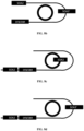
- the DFB or DBR laser and the second gain region SOA2 can be simultaneously integrated on both sides of the FP resonant cavity respectively, and an additional SOA3 (as shown in FIG. 8a ) or SOA3' (as shown in FIG.
- the SOA3' is a PN junction region or MOS junction region
- the additional PN junction region or MOS junction region SOA3' may be formed by performing modification processing or alteration treatment on the third gain region SOA3, or can be formed by depositing a dielectric film and a semiconductor material after removing the third gain region part
- the additional PN junction region or MOS junction region SOA3' is transparent to the lasing wavelength; by performing electric injection or reverse bias on the additional PN junction region or MOS junction region SOA3', rapidly frequency-modulated and narrow linewidth laser with low power consumption can be achieved.
- the DFB or DBR laser and the second gain region SOA2 can be integrated on the same side of the FP resonant cavity respectively, and an additional SOA3 (as shown in FIG. 8c ) or SOA3' (as shown in FIG. 8d ) can be embedded in the M-Z compound external cavity structure with a view of achieving high-power narrow linewidth frequency-modulated laser.
- the devices of the first embodiment to the eighth embodiment can be achieved based on a semiconductor optoelectronic device substrate and a semiconductor monolithic integration technology or a hybrid integration technology thereon.
- the method for fabricating any of the above-mentioned narrow linewidth lasers by the monolithic integration technology may comprises the following steps:
- a method for fabricating any of the previous narrow linewidth lasers by the monolithic integration technology may comprises the following steps:
- the procedure of modifying the third gain region SOA3 can also be added to convert the third gain region to be transparent to the lasing light of the device, by which, the electrically injected or reverse biased PN junction or MOS junction can be achieved, and the device configurations shown in FIG. 7 or FIG. 8b or FIG. 8d should be obtained.
- an anti-reflection film can be deposited at a light-emitting facet of a fabricated chip to avoid residual reflection, and a high-reflection film can be deposited on one side of a non-light-emitting facet to enhance light feedback, thus narrowing the linewidth and suppressing the noise.
- the narrow linewidth laser provided by the embodiments of the present disclosure is simple in waveguide structure, simple in tuning management, and it is expected to obtain broadband rapidly tuning with low power consumption, high side-mode suppression ratio, and narrow linewidth.
- the monolithically integrated narrow linewidth laser formed by the embodiments of the present disclosure at least has the following advantages: 1 coupling loss of the external cavity and the gain region can be greatly eliminated, thus effectively reducing a threshold value and narrowing linewidth; 2 the same material has similar thermal and mechanical properties, thus the device is good in stability and reliability and has the increased susceptibility to severe environment; 3 the devices are uniform and low cost due to their batch design and fabrication; 4 it is expected to achieve electric tuning, high tuning speed, good tuning linearity, and low tuning power consumption.
- FIG. 11 is a spectrum of a laser in an embodiment as shown in FIG. 3 . It can be known that the laser has a high side-mode suppression ratio and broadband tuning function.
- FIG. 12 is a frequency noise spectrum of the laser, and based on the noise level at 10MHz frequency section of this frequency noise spectrum, it can be extracted that the laser has a Lorentzian linewidth of the order of kHz level.
- the device can also be achieved through butt-joint integration, optical micro-assembling and other technical solutions, while the basic configuration of the device is to be presented as a semiconductor gain chip and an M-Z compound external cavity structure formed by coupling the FP resonant cavity and the ring resonant cavity, wherein the gain chip of the device can be any gain unit with required wavelengths, which comprises but is not limited to semiconductor gain chips with various substrates and wavelength ranges, an optical fiber gain unit, a solid (gas) gain unit and the like; the M-Z compound external cavity can be In(AlGa)As(P) waveguide, SOI waveguide, Si waveguide, SiN waveguide, SiNO waveguide and any other waveguide structure which is transparent and low loss with respect to the gain units, thus guaranteeing that the broadband tunable narrow linewidth laser can be achieved; wherein the gain region SOA1 part may select a semiconductor optical amplifier, a DFB laser or a DBR laser; and SO
Landscapes
- Physics & Mathematics (AREA)
- General Physics & Mathematics (AREA)
- Optics & Photonics (AREA)
- Condensed Matter Physics & Semiconductors (AREA)
- Electromagnetism (AREA)
- Nonlinear Science (AREA)
- Semiconductor Lasers (AREA)
Claims (9)
- Laser mit schmaler Linienbreite, umfassend einen passiven Ringresonanzhohlraum, einen U-förmigen Fabry-Pérot-(FP)-Resonanzhohlraum, der den passiven Ringresonanzhohlraum umhüllt, und einen ersten Verstärkungsbereich (SOA1), wobei der passive Ringresonanzhohlraum und der FP-Resonanzhohlraum kombiniert werden, um eine externe Mach-Zehnder-(M-Z)-Verbundhohlraumstruktur zu bilden, sodass zwei freie Enden des U-förmigen FP-Resonanzhohlraums jeweils ein erstes Ende und ein zweites Ende der externen M-Z-Verbundhohlraumstruktur bilden, wobei das erste Ende im ersten Verstärkungsbereich (SOA1) bereitgestellt ist, ein direkter und kontinuierlicher Übertragungsweg rund um den passiven Ringresonanzhohlraum zwischen dem ersten Ende und dem zweiten Ende der externen M-Z-Verbundhohlraumstruktur gebildet wird, um eine Übertragung direkt vom ersten Ende zum zweiten Ende oder vom zweiten Ende zum ersten Ende zu ermöglichen, die externe M-Z-Verbundhohlraumstruktur zumindest zur Bereitstellung der Wellenlängenauswahl und Verengung der Laserlinienbreite verwendet wird und der erste Verstärkungsbereich (SOA1) auf der äußeren Seite der externen M-Z-Verbundhohlraumstruktur bereitgestellt ist und zumindest verwendet wird, um eine Verstärkung für den gesamten Laser bereitzustellen.
- Laser mit schmaler Linienbreite nach Anspruch 1, wobei der passive Ringresonanzhohlraum und der FP-Resonanzhohlraum parallel gekoppelt sind, um die externe M-Z-Verbundhohlraumstruktur zu bilden, und/oder ein Brechungsindex eines Wellenleiters entweder des passiven Ringresonanzhohlraums oder des FP-Resonanzhohlraums einstellbar ist, wodurch eine Wellenlängenabstimmungsfunktion erreicht wird.
- Laser mit schmaler Linienbreite nach Anspruch 1, zudem umfassend einen zweiten Verstärkungsbereich (SOA2), wobei der zweite Verstärkungsbereich (SOA2) auf der äußeren Seite der externen M-Z-Verbundhohlraumstruktur bereitgestellt ist und zumindest zur Verstärkung von Laserlicht, Verbesserung der Ausgangsleistung, Optimierung des optischen Feedbacks und weiteren Verengung der Laserlinienbreite und Unterdrückung des Rauschens verwendet wird.
- Laser mit schmaler Linienbreite nach Anspruch 3, wobei der Laser eine monolithisch integrierte Konfiguration aufweist, wobei der erste Verstärkungsbereich (SOA1) zudem mit einer Gitterstruktur versehen ist, die einen Laser mit verteilter Rückkopplung (DFB) oder einen Distributed-Bragg-(DBR)-Laser zusammen mit dem ersten Verstärkungsbereich (SOA1) bildet, wobei der zweite Verstärkungsbereich (SOA2) einen optischen Halbleiterverstärker umfasst, die Laserkonfiguration eine heterogen integrierte Konfiguration, eine integrierte Stoßgelenkkonfiguration oder eine mikrokonfektionierte integrierte Konfiguration umfasst, der erste Verstärkungsbereich (SOA1) in all diesen Konfigurationen den DFB-Laser oder den DBR-Laser umfasst und der zweite Verstärkungsbereich (SOA2) einen optischen Halbleiterverstärker umfasst.
- Laser mit schmaler Linienbreite nach Anspruch 4, wobei der Laser eine monolithisch integrierte Konfiguration aufweist, deren monolithische Integration durch eine der Technologien der Quantentopfvermischung, der Stoßgelenkepitaxie, der selektiven Flächenepitaxie und der vertikalen Kopplungsintegration erreicht wird.
- Laser mit schmaler Linienbreite nach Anspruch 3, der zudem einen zusätzlichen PN-Verbindungsbereich oder einen MOS-Verbindungsbereich (SOA3') umfasst, wobei der zusätzliche PN-Verbindungsbereich oder MOS-Verbindungsbereich (SOA3') in die externe M-Z-Verbundhohlraumstruktur eingebettet ist, der zusätzliche PN-Verbindungsbereich ein Verstärkungsbereich ist und zumindest verwendet wird, um den Verlust der externen M-Z-Verbundhohlraumstruktur zu kompensieren und somit den optischen Weg eines externen Hohlraums zu verlängern, die optische negative Rückkopplung zu verbessern und die Laserlinienbreite zu verengen, oder der zusätzliche PN-Verbindungsbereich oder MOS-Verbindungsbereich (SOA3') für die Laserwellenlänge transparent ist und ein Brechungsindex des zusätzlichen PN-Verbindungsbereichs oder MOS-Verbindungsbereichs (SOA3') schnell eingestellt werden, wenn eine elektrische Injektion oder eine Rückwärtsvorspannung auf dem zusätzlichen PN-Verbindungsbereich oder dem MOS-Verbindungsbereich durchgeführt wird, wodurch eine schnelle Abstimmung der Laserwellenlänge bei geringerem Stromverbrauch erreicht wird.
- Laser mit schmaler Linienbreite nach Anspruch 6, wobei der Laser eine monolithisch integrierte Konfiguration aufweist und der erste Verstärkungsbereich (SOA1) zudem mit einer Gitterstruktur versehen ist, die einen Laser mit verteilter Rückkopplung (DFB) oder einen Distributed-Bragg-(DBR)-Laser zusammen mit dem ersten Verstärkungsbereich (SOA1) bildet, wobei der zweite Verstärkungsbereich (SOA2) einen optischen Halbleiterverstärker umfasst, der zusätzliche PN-Verbindungsbereich einen optischen Halbleiterverstärker oder einen Wellenleiter, der für das Laserlicht transparent ist, umfasst, der zusätzliche MOS-Verbindungsbereich einen Wellenleiter, der für die Laserwellenlänge transparent ist, umfasst, die Laserkonfiguration eine heterogen integrierte Konfiguration, eine integrierte Stoßgelenkkonfiguration oder eine mikrokonfektionierte integrierte Konfiguration umfasst, der erste Verstärkungsbereich (SOA1) in all diesen Konfigurationen den DFB-Laser oder den DBR-Laser umfasst, der zweite Verstärkungsbereich (SOA2) den optischen Halbleiterverstärker umfasst, der zusätzliche PN-Verbindungsbereich den optischen Halbleiterverstärker oder einen Wellenleiter umfasst, der transparent für das Laserlicht ist, oder der zusätzliche MOS-Verbindungsbereich ein Wellenleiter ist, der transparent für das Laserlicht ist.
- Laser mit schmaler Linienbreite nach Anspruch 4, wobei der Laser durch Kombinieren eines Halbleiterverstärkungschips und der externen M-Z-Verbundhohlraumstruktur gebildet ist, die durch parallele Kopplung des FP-Resonanzhohlraums und des passiven Ringresonanzhohlraums gebildet ist.
- Laser mit schmaler Linienbreite nach Anspruch 8, wobei die externe M-Z-Verbundhohlraumstruktur eine verlustarme Wellenleiterstruktur ist, die verlustarme Wellenleiterstruktur einen Wellenleiter umfasst, der aus demselben System von Materialien besteht, das in Bezug auf ein Verstärkungsmaterial transparent ist, oder einen Wellenleiter, der aus einem anderen System von Materialien als der Verstärkungsbereich besteht, oder einen Wellenleiter, der aus einer Mischung aus demselben System von Materialien und dem unterschiedlichen Materialsystem besteht, vorzugsweise einen InP-, GaAs-basierten In(Ga)As(P)-Wellenleiter, einen InGa(Al)As(P)-Wellenleiter, einen SOI-basierten Si-Wellenleiter, einen SiN-Wellenleiter, einen Lithiumniobat-Wellenleiter, einen SiNO-Wellenleiter, einen SiO2-Wellenleiter, einen In(Ga)As(P)/Si- oder Si/SiO2/InGaAsP-Hybridwellenleiter.
Applications Claiming Priority (2)
| Application Number | Priority Date | Filing Date | Title |
|---|---|---|---|
| CN202011316288.5A CN114552378B (zh) | 2020-11-20 | 2020-11-20 | 窄线宽激光器 |
| PCT/CN2021/131821 WO2022105883A1 (zh) | 2020-11-20 | 2021-11-19 | 窄线宽激光器 |
Publications (3)
| Publication Number | Publication Date |
|---|---|
| EP4178053A1 EP4178053A1 (de) | 2023-05-10 |
| EP4178053A4 EP4178053A4 (de) | 2024-01-24 |
| EP4178053B1 true EP4178053B1 (de) | 2025-06-11 |
Family
ID=81660495
Family Applications (1)
| Application Number | Title | Priority Date | Filing Date |
|---|---|---|---|
| EP21894030.2A Active EP4178053B1 (de) | 2020-11-20 | 2021-11-19 | Laser mit schmaler linienbreite |
Country Status (5)
| Country | Link |
|---|---|
| US (1) | US11901699B2 (de) |
| EP (1) | EP4178053B1 (de) |
| JP (1) | JP7517738B2 (de) |
| CN (1) | CN114552378B (de) |
| WO (1) | WO2022105883A1 (de) |
Families Citing this family (4)
| Publication number | Priority date | Publication date | Assignee | Title |
|---|---|---|---|---|
| GB2602963B (en) * | 2020-12-31 | 2025-03-26 | Smart Photonics Holding B V | Semiconductor structure for photonic integrated circuit and method of manufacture |
| CN116131096A (zh) * | 2023-02-06 | 2023-05-16 | 中国科学院半导体研究所 | 宽调谐窄线宽半导体激光器 |
| CN116316057A (zh) * | 2023-02-24 | 2023-06-23 | 浙江大学 | 一种基于马赫泽德干涉仪的窄线宽半导体激光器芯片 |
| CN117895322B (zh) * | 2024-03-18 | 2024-08-06 | 北京弘光向尚科技有限公司 | 一种减少外腔可调谐激光器跳模现象的方法 |
Family Cites Families (46)
| Publication number | Priority date | Publication date | Assignee | Title |
|---|---|---|---|---|
| US368654A (en) | 1887-08-23 | Electric hose-coupling | ||
| US549347A (en) | 1895-11-05 | Wesley clark | ||
| US276763A (en) | 1883-05-01 | beock | ||
| US408739A (en) | 1889-08-13 | Anders gustav nyblin | ||
| US4720160A (en) * | 1981-12-16 | 1988-01-19 | Polaroid Corporation | Optical resonant cavity filters |
| CN86202829U (zh) | 1986-05-08 | 1987-06-10 | 清华大学 | 外腔粘接型窄线宽单模半导体激光器 |
| US20030002548A1 (en) | 2000-12-21 | 2003-01-02 | Bogie Boscha | Laser-diode assembly with external bragg grating for narrow-bandwidth light and a method of narrowing linewidth of the spectrum |
| US6690687B2 (en) * | 2001-01-02 | 2004-02-10 | Spectrasensors, Inc. | Tunable semiconductor laser having cavity with ring resonator mirror and mach-zehnder interferometer |
| US6856641B2 (en) * | 2001-01-26 | 2005-02-15 | California Institute Of Technology | Ring resonator based narrow-linewidth semiconductor lasers |
| AU2003253750A1 (en) * | 2002-06-28 | 2004-01-19 | California Institute Of Technology | Optical resonator and laser applications |
| EP1420284A1 (de) * | 2002-11-14 | 2004-05-19 | Avanex Corporation | Verfahren zum Einstellen der Doppelbrechung von integrierten optischen Vorrichtungen durch Oberflächenerhitzung |
| CN2687911Y (zh) | 2003-12-31 | 2005-03-23 | 南开大学 | 可调谐光栅外腔半导体激光器 |
| TWI251393B (en) * | 2004-03-31 | 2006-03-11 | Nec Corp | Tunable laser |
| CN100416948C (zh) | 2005-06-27 | 2008-09-03 | 北京理工大学 | 一种窄线宽单频光纤激光器 |
| US20090092159A1 (en) * | 2007-05-28 | 2009-04-09 | Sumitomo Electric Industries, Ltd. | Semiconductor light-emitting device with tunable emission wavelength |
| CN101521352B (zh) | 2008-02-28 | 2012-07-04 | 中国计量科学研究院 | 半导体激光器 |
| US7649384B2 (en) | 2008-02-05 | 2010-01-19 | Broadcom Corporation | High-voltage tolerant output driver |
| US8885675B2 (en) * | 2008-03-26 | 2014-11-11 | Nec Corporation | Wavelength variable laser device, and method and program for controlling the same |
| US8058143B2 (en) | 2009-01-21 | 2011-11-15 | Freescale Semiconductor, Inc. | Substrate bonding with metal germanium silicon material |
| CN101881917A (zh) | 2009-05-07 | 2010-11-10 | 胡宗福 | 基于光纤环形腔内光相位调制和光放大的相干多波长光源 |
| CN102035136B (zh) | 2009-09-29 | 2014-07-30 | 中国计量科学研究院 | 一种外腔半导体激光器 |
| JP2012114163A (ja) * | 2010-11-22 | 2012-06-14 | Nec Corp | 光ファイバ通信用波長可変半導体レーザ光源 |
| CN103733448B (zh) * | 2011-08-10 | 2016-08-17 | 富士通株式会社 | 半导体光元件 |
| EP2570799A1 (de) * | 2011-09-19 | 2013-03-20 | Fraunhofer Gesellschaft zur Förderung der angewandten Wissenschaft E.V. | Optische Sensoranordnung und Verfahren zum Messen einer Observable |
| US9692207B2 (en) | 2011-09-30 | 2017-06-27 | Aurrion, Inc. | Tunable laser with integrated wavelength reference |
| CN202260110U (zh) | 2011-09-30 | 2012-05-30 | 杭州电子科技大学 | 一种窄线宽可调谐的多波长光纤激光器 |
| WO2013114577A1 (ja) * | 2012-01-31 | 2013-08-08 | 富士通株式会社 | レーザ素子 |
| CN102931582A (zh) | 2012-07-25 | 2013-02-13 | 华中科技大学 | 可调谐光栅外腔半导体激光器 |
| CN202917803U (zh) | 2012-11-29 | 2013-05-01 | 合肥知常光电科技有限公司 | 一种可调谐窄线宽皮秒脉冲激光器 |
| CN103022864B (zh) | 2012-12-13 | 2014-12-03 | 华南理工大学 | 一种可调谐窄线宽阵列单频光纤激光器 |
| CN103441423B (zh) | 2013-09-02 | 2016-02-10 | 中国电子科技集团公司第三十四研究所 | 窄线宽可调激光器系统及运行方法 |
| CN103594911A (zh) | 2013-11-04 | 2014-02-19 | 中国科学院苏州生物医学工程技术研究所 | 一种ld泵浦全固体分布反馈型窄线宽激光器 |
| CN203690693U (zh) | 2013-11-29 | 2014-07-02 | 中国科学院西安光学精密机械研究所 | 高速宽带窄线宽扫频全光纤激光器 |
| CN103682979B (zh) | 2013-12-26 | 2016-08-17 | 中国科学院半导体研究所 | 窄线宽稳频半导体激光器 |
| FR3020188A1 (fr) * | 2014-04-18 | 2015-10-23 | Commissariat Energie Atomique | Source laser |
| CN104092086A (zh) | 2014-06-18 | 2014-10-08 | 华南理工大学 | 一种超窄线宽单频调q脉冲光纤激光器 |
| CN104143757B (zh) | 2014-08-07 | 2017-03-08 | 中国科学院半导体研究所 | 基于分布布拉格反射激光器的波长可调谐窄线宽光源 |
| CN104300358A (zh) | 2014-09-22 | 2015-01-21 | 江苏骏龙电力科技股份有限公司 | 宽范围相位连续扫频的窄线宽激光光源 |
| CN104319623A (zh) | 2014-10-31 | 2015-01-28 | 中国科学院半导体研究所 | 基于偏振反馈的超窄线宽半导体激光器装置 |
| CN204243445U (zh) | 2014-11-17 | 2015-04-01 | 山东海富光子科技股份有限公司 | 一种高功率窄线宽线偏振光纤激光器 |
| JP6545020B2 (ja) * | 2015-06-30 | 2019-07-17 | 富士通株式会社 | 変調光源 |
| CN105322438B (zh) * | 2015-12-11 | 2018-09-18 | 武汉邮电科学研究院 | 一种基于硅基的窄线宽可调外腔激光器 |
| JP6588851B2 (ja) * | 2016-03-24 | 2019-10-09 | 日本電信電話株式会社 | 外部共振器型レーザ光源 |
| CN108075354A (zh) * | 2016-11-14 | 2018-05-25 | 中国科学院苏州纳米技术与纳米仿生研究所 | 窄线宽激光器 |
| EP3840138A1 (de) * | 2019-12-17 | 2021-06-23 | FRAUNHOFER-GESELLSCHAFT zur Förderung der angewandten Forschung e.V. | Dwdm-intra-resonator-laservorrichtung |
| CN111613959B (zh) * | 2020-04-10 | 2021-12-03 | 清华大学 | 基于硅基外腔自注入的窄线宽连续波调频激光器 |
-
2020
- 2020-11-20 CN CN202011316288.5A patent/CN114552378B/zh active Active
-
2021
- 2021-11-19 JP JP2022570280A patent/JP7517738B2/ja active Active
- 2021-11-19 EP EP21894030.2A patent/EP4178053B1/de active Active
- 2021-11-19 US US17/928,934 patent/US11901699B2/en active Active
- 2021-11-19 WO PCT/CN2021/131821 patent/WO2022105883A1/zh not_active Ceased
Also Published As
| Publication number | Publication date |
|---|---|
| CN114552378B (zh) | 2023-03-31 |
| JP2023525594A (ja) | 2023-06-16 |
| CN114552378A (zh) | 2022-05-27 |
| US11901699B2 (en) | 2024-02-13 |
| WO2022105883A1 (zh) | 2022-05-27 |
| EP4178053A4 (de) | 2024-01-24 |
| EP4178053A1 (de) | 2023-05-10 |
| JP7517738B2 (ja) | 2024-07-17 |
| US20230261440A1 (en) | 2023-08-17 |
Similar Documents
| Publication | Publication Date | Title |
|---|---|---|
| US11901699B2 (en) | Narrow linewidth laser | |
| US10680410B2 (en) | External cavity laser | |
| US9343614B2 (en) | Superluminescent diode, method of manufacturing the same, and wavelength-tunable external cavity laser including the same | |
| CN113557643A (zh) | 硅光子外腔可调谐激光器的波长控制方法 | |
| US8005123B2 (en) | Wavelength tunable laser | |
| Le Liepvre et al. | Widely wavelength tunable hybrid III–V/silicon laser with 45 nm tuning range fabricated using a wafer bonding technique | |
| US20090225796A1 (en) | Diffraction grating device, laser diode, and wavelength tunable filter | |
| US10992107B2 (en) | Narrow-linewidth laser | |
| US20230411929A1 (en) | Narrow linewidth semiconductor laser | |
| CN117498135A (zh) | 大范围波长调谐激光器 | |
| Kim et al. | Total internal reflection mirror-based InGaAsP ring resonators integrated with optical amplifiers | |
| CN105281199B (zh) | 频率间隔连续可调的v型耦合腔双波长半导体激光器 | |
| Hao et al. | High-speed directly modulated widely tunable hybrid square/rhombus-rectangular coupled cavity lasers | |
| Wang et al. | Widely tunable narrow-linewidth laser based on a multi-period-delayed feedback photonic circuit | |
| Wu et al. | Wavelength switchable semiconductor laser based on half-wave coupled Fabry–Pérot and rectangular ring resonators | |
| CN107104362A (zh) | 半导体激光二极管及其制造方法 | |
| US20050226283A1 (en) | Single-mode semiconductor laser with integrated optical waveguide filter | |
| JP6083644B2 (ja) | 集積型半導体光源 | |
| Kim et al. | Widely tunable coupled-ring reflector laser diode consisting of square ring resonators | |
| US20250055254A1 (en) | Semiconductor Laser | |
| US12197003B2 (en) | Optical filter and wavelength tunable laser element | |
| CN205122996U (zh) | 一种频率间隔连续可调的v型耦合腔双波长半导体激光器 | |
| Oberg et al. | InGaAsP-InP laser amplifier with integrated passive waveguides | |
| Li et al. | Hertz-linewidth hybrid integrated laser based on high-Q Si3N4 microring reflectors | |
| Guo et al. | High-performance III-V/Si3N4 O-band external cavity tunable laser |
Legal Events
| Date | Code | Title | Description |
|---|---|---|---|
| STAA | Information on the status of an ep patent application or granted ep patent |
Free format text: STATUS: THE INTERNATIONAL PUBLICATION HAS BEEN MADE |
|
| PUAI | Public reference made under article 153(3) epc to a published international application that has entered the european phase |
Free format text: ORIGINAL CODE: 0009012 |
|
| STAA | Information on the status of an ep patent application or granted ep patent |
Free format text: STATUS: REQUEST FOR EXAMINATION WAS MADE |
|
| 17P | Request for examination filed |
Effective date: 20230131 |
|
| AK | Designated contracting states |
Kind code of ref document: A1 Designated state(s): AL AT BE BG CH CY CZ DE DK EE ES FI FR GB GR HR HU IE IS IT LI LT LU LV MC MK MT NL NO PL PT RO RS SE SI SK SM TR |
|
| A4 | Supplementary search report drawn up and despatched |
Effective date: 20240102 |
|
| RIC1 | Information provided on ipc code assigned before grant |
Ipc: H01S 5/50 20060101ALI20231219BHEP Ipc: H01S 5/026 20060101ALI20231219BHEP Ipc: H01S 5/12 20210101ALI20231219BHEP Ipc: H01S 5/125 20060101ALI20231219BHEP Ipc: H01S 5/14 20060101AFI20231219BHEP |
|
| DAV | Request for validation of the european patent (deleted) | ||
| DAX | Request for extension of the european patent (deleted) | ||
| GRAP | Despatch of communication of intention to grant a patent |
Free format text: ORIGINAL CODE: EPIDOSNIGR1 |
|
| STAA | Information on the status of an ep patent application or granted ep patent |
Free format text: STATUS: GRANT OF PATENT IS INTENDED |
|
| INTG | Intention to grant announced |
Effective date: 20250212 |
|
| GRAS | Grant fee paid |
Free format text: ORIGINAL CODE: EPIDOSNIGR3 |
|
| GRAA | (expected) grant |
Free format text: ORIGINAL CODE: 0009210 |
|
| STAA | Information on the status of an ep patent application or granted ep patent |
Free format text: STATUS: THE PATENT HAS BEEN GRANTED |
|
| AK | Designated contracting states |
Kind code of ref document: B1 Designated state(s): AL AT BE BG CH CY CZ DE DK EE ES FI FR GB GR HR HU IE IS IT LI LT LU LV MC MK MT NL NO PL PT RO RS SE SI SK SM TR |
|
| REG | Reference to a national code |
Ref country code: GB Ref legal event code: FG4D |
|
| REG | Reference to a national code |
Ref country code: CH Ref legal event code: EP |
|
| REG | Reference to a national code |
Ref country code: IE Ref legal event code: FG4D |
|
| REG | Reference to a national code |
Ref country code: DE Ref legal event code: R096 Ref document number: 602021032267 Country of ref document: DE |
|
| P01 | Opt-out of the competence of the unified patent court (upc) registered |
Free format text: CASE NUMBER: APP_28722/2025 Effective date: 20250616 |
|
| PG25 | Lapsed in a contracting state [announced via postgrant information from national office to epo] |
Ref country code: ES Free format text: LAPSE BECAUSE OF FAILURE TO SUBMIT A TRANSLATION OF THE DESCRIPTION OR TO PAY THE FEE WITHIN THE PRESCRIBED TIME-LIMIT Effective date: 20250611 Ref country code: FI Free format text: LAPSE BECAUSE OF FAILURE TO SUBMIT A TRANSLATION OF THE DESCRIPTION OR TO PAY THE FEE WITHIN THE PRESCRIBED TIME-LIMIT Effective date: 20250611 |
|
| REG | Reference to a national code |
Ref country code: LT Ref legal event code: MG9D |
|
| PG25 | Lapsed in a contracting state [announced via postgrant information from national office to epo] |
Ref country code: GR Free format text: LAPSE BECAUSE OF FAILURE TO SUBMIT A TRANSLATION OF THE DESCRIPTION OR TO PAY THE FEE WITHIN THE PRESCRIBED TIME-LIMIT Effective date: 20250912 Ref country code: NO Free format text: LAPSE BECAUSE OF FAILURE TO SUBMIT A TRANSLATION OF THE DESCRIPTION OR TO PAY THE FEE WITHIN THE PRESCRIBED TIME-LIMIT Effective date: 20250911 |
|
| REG | Reference to a national code |
Ref country code: NL Ref legal event code: MP Effective date: 20250611 |
|
| PG25 | Lapsed in a contracting state [announced via postgrant information from national office to epo] |
Ref country code: BG Free format text: LAPSE BECAUSE OF FAILURE TO SUBMIT A TRANSLATION OF THE DESCRIPTION OR TO PAY THE FEE WITHIN THE PRESCRIBED TIME-LIMIT Effective date: 20250611 |
|
| PG25 | Lapsed in a contracting state [announced via postgrant information from national office to epo] |
Ref country code: HR Free format text: LAPSE BECAUSE OF FAILURE TO SUBMIT A TRANSLATION OF THE DESCRIPTION OR TO PAY THE FEE WITHIN THE PRESCRIBED TIME-LIMIT Effective date: 20250611 |
|
| PG25 | Lapsed in a contracting state [announced via postgrant information from national office to epo] |
Ref country code: RS Free format text: LAPSE BECAUSE OF FAILURE TO SUBMIT A TRANSLATION OF THE DESCRIPTION OR TO PAY THE FEE WITHIN THE PRESCRIBED TIME-LIMIT Effective date: 20250911 |
|
| PG25 | Lapsed in a contracting state [announced via postgrant information from national office to epo] |
Ref country code: LV Free format text: LAPSE BECAUSE OF FAILURE TO SUBMIT A TRANSLATION OF THE DESCRIPTION OR TO PAY THE FEE WITHIN THE PRESCRIBED TIME-LIMIT Effective date: 20250611 |
|
| PG25 | Lapsed in a contracting state [announced via postgrant information from national office to epo] |
Ref country code: NL Free format text: LAPSE BECAUSE OF FAILURE TO SUBMIT A TRANSLATION OF THE DESCRIPTION OR TO PAY THE FEE WITHIN THE PRESCRIBED TIME-LIMIT Effective date: 20250611 |
|
| PG25 | Lapsed in a contracting state [announced via postgrant information from national office to epo] |
Ref country code: PT Free format text: LAPSE BECAUSE OF FAILURE TO SUBMIT A TRANSLATION OF THE DESCRIPTION OR TO PAY THE FEE WITHIN THE PRESCRIBED TIME-LIMIT Effective date: 20251013 |
|
| REG | Reference to a national code |
Ref country code: AT Ref legal event code: MK05 Ref document number: 1803025 Country of ref document: AT Kind code of ref document: T Effective date: 20250611 |
|
| PG25 | Lapsed in a contracting state [announced via postgrant information from national office to epo] |
Ref country code: IS Free format text: LAPSE BECAUSE OF FAILURE TO SUBMIT A TRANSLATION OF THE DESCRIPTION OR TO PAY THE FEE WITHIN THE PRESCRIBED TIME-LIMIT Effective date: 20251011 |
|
| PGFP | Annual fee paid to national office [announced via postgrant information from national office to epo] |
Ref country code: DE Payment date: 20251117 Year of fee payment: 5 |
|
| PGFP | Annual fee paid to national office [announced via postgrant information from national office to epo] |
Ref country code: GB Payment date: 20251126 Year of fee payment: 5 |
|
| PG25 | Lapsed in a contracting state [announced via postgrant information from national office to epo] |
Ref country code: AT Free format text: LAPSE BECAUSE OF FAILURE TO SUBMIT A TRANSLATION OF THE DESCRIPTION OR TO PAY THE FEE WITHIN THE PRESCRIBED TIME-LIMIT Effective date: 20250611 Ref country code: SM Free format text: LAPSE BECAUSE OF FAILURE TO SUBMIT A TRANSLATION OF THE DESCRIPTION OR TO PAY THE FEE WITHIN THE PRESCRIBED TIME-LIMIT Effective date: 20250611 |
|
| PGFP | Annual fee paid to national office [announced via postgrant information from national office to epo] |
Ref country code: FR Payment date: 20251127 Year of fee payment: 5 |
|
| PG25 | Lapsed in a contracting state [announced via postgrant information from national office to epo] |
Ref country code: CZ Free format text: LAPSE BECAUSE OF FAILURE TO SUBMIT A TRANSLATION OF THE DESCRIPTION OR TO PAY THE FEE WITHIN THE PRESCRIBED TIME-LIMIT Effective date: 20250611 |
|
| PG25 | Lapsed in a contracting state [announced via postgrant information from national office to epo] |
Ref country code: PL Free format text: LAPSE BECAUSE OF FAILURE TO SUBMIT A TRANSLATION OF THE DESCRIPTION OR TO PAY THE FEE WITHIN THE PRESCRIBED TIME-LIMIT Effective date: 20250611 |
|
| PG25 | Lapsed in a contracting state [announced via postgrant information from national office to epo] |
Ref country code: EE Free format text: LAPSE BECAUSE OF FAILURE TO SUBMIT A TRANSLATION OF THE DESCRIPTION OR TO PAY THE FEE WITHIN THE PRESCRIBED TIME-LIMIT Effective date: 20250611 |
|
| PG25 | Lapsed in a contracting state [announced via postgrant information from national office to epo] |
Ref country code: SK Free format text: LAPSE BECAUSE OF FAILURE TO SUBMIT A TRANSLATION OF THE DESCRIPTION OR TO PAY THE FEE WITHIN THE PRESCRIBED TIME-LIMIT Effective date: 20250611 |
|
| PG25 | Lapsed in a contracting state [announced via postgrant information from national office to epo] |
Ref country code: RO Free format text: LAPSE BECAUSE OF FAILURE TO SUBMIT A TRANSLATION OF THE DESCRIPTION OR TO PAY THE FEE WITHIN THE PRESCRIBED TIME-LIMIT Effective date: 20250611 |
|
| REG | Reference to a national code |
Ref country code: DE Ref legal event code: R097 Ref document number: 602021032267 Country of ref document: DE |
|
| PG25 | Lapsed in a contracting state [announced via postgrant information from national office to epo] |
Ref country code: DK Free format text: LAPSE BECAUSE OF FAILURE TO SUBMIT A TRANSLATION OF THE DESCRIPTION OR TO PAY THE FEE WITHIN THE PRESCRIBED TIME-LIMIT Effective date: 20250611 |
|
| PG25 | Lapsed in a contracting state [announced via postgrant information from national office to epo] |
Ref country code: IT Free format text: LAPSE BECAUSE OF FAILURE TO SUBMIT A TRANSLATION OF THE DESCRIPTION OR TO PAY THE FEE WITHIN THE PRESCRIBED TIME-LIMIT Effective date: 20250611 |
|
| PLBE | No opposition filed within time limit |
Free format text: ORIGINAL CODE: 0009261 |
|
| STAA | Information on the status of an ep patent application or granted ep patent |
Free format text: STATUS: NO OPPOSITION FILED WITHIN TIME LIMIT |
|
| REG | Reference to a national code |
Ref country code: CH Ref legal event code: L10 Free format text: ST27 STATUS EVENT CODE: U-0-0-L10-L00 (AS PROVIDED BY THE NATIONAL OFFICE) Effective date: 20260423 |