EP4178166A2 - Unité d'adaptateur et procédé de couplage d'une unité d'évaluation à un bus de données ainsi que système et véhicule dotés d'une unité d'adaptateur correspondante - Google Patents
Unité d'adaptateur et procédé de couplage d'une unité d'évaluation à un bus de données ainsi que système et véhicule dotés d'une unité d'adaptateur correspondante Download PDFInfo
- Publication number
- EP4178166A2 EP4178166A2 EP22204237.6A EP22204237A EP4178166A2 EP 4178166 A2 EP4178166 A2 EP 4178166A2 EP 22204237 A EP22204237 A EP 22204237A EP 4178166 A2 EP4178166 A2 EP 4178166A2
- Authority
- EP
- European Patent Office
- Prior art keywords
- bus
- data
- unit
- signal
- adapter unit
- Prior art date
- Legal status (The legal status is an assumption and is not a legal conclusion. Google has not performed a legal analysis and makes no representation as to the accuracy of the status listed.)
- Withdrawn
Links
- 230000008878 coupling Effects 0.000 title claims abstract description 64
- 238000010168 coupling process Methods 0.000 title claims abstract description 64
- 238000005859 coupling reaction Methods 0.000 title claims abstract description 64
- 238000011156 evaluation Methods 0.000 title claims abstract description 46
- 238000000034 method Methods 0.000 title claims abstract description 14
- 239000004020 conductor Substances 0.000 claims abstract description 130
- 238000012545 processing Methods 0.000 claims abstract description 17
- 230000015654 memory Effects 0.000 claims description 23
- 238000012360 testing method Methods 0.000 claims description 12
- 238000004088 simulation Methods 0.000 claims description 9
- 230000003750 conditioning effect Effects 0.000 claims description 5
- 230000001143 conditioned effect Effects 0.000 claims description 4
- 238000012937 correction Methods 0.000 claims description 3
- 230000008569 process Effects 0.000 abstract description 5
- 230000005540 biological transmission Effects 0.000 description 18
- 238000004891 communication Methods 0.000 description 9
- 230000008901 benefit Effects 0.000 description 8
- 238000009434 installation Methods 0.000 description 6
- 238000005516 engineering process Methods 0.000 description 5
- 230000006870 function Effects 0.000 description 5
- 230000003287 optical effect Effects 0.000 description 5
- 229910052802 copper Inorganic materials 0.000 description 4
- 239000010949 copper Substances 0.000 description 4
- RYGMFSIKBFXOCR-UHFFFAOYSA-N Copper Chemical compound [Cu] RYGMFSIKBFXOCR-UHFFFAOYSA-N 0.000 description 3
- 230000006978 adaptation Effects 0.000 description 3
- 230000006399 behavior Effects 0.000 description 3
- 230000008859 change Effects 0.000 description 3
- 238000006243 chemical reaction Methods 0.000 description 3
- 238000013461 design Methods 0.000 description 3
- 238000001514 detection method Methods 0.000 description 3
- 230000000694 effects Effects 0.000 description 3
- 238000011161 development Methods 0.000 description 2
- 230000018109 developmental process Effects 0.000 description 2
- 238000010586 diagram Methods 0.000 description 2
- 230000005684 electric field Effects 0.000 description 2
- 238000004519 manufacturing process Methods 0.000 description 2
- 238000003860 storage Methods 0.000 description 2
- 238000013024 troubleshooting Methods 0.000 description 2
- 238000004458 analytical method Methods 0.000 description 1
- 238000013475 authorization Methods 0.000 description 1
- 230000015572 biosynthetic process Effects 0.000 description 1
- 230000006835 compression Effects 0.000 description 1
- 238000007906 compression Methods 0.000 description 1
- 150000001879 copper Chemical class 0.000 description 1
- 230000001808 coupling effect Effects 0.000 description 1
- 238000012217 deletion Methods 0.000 description 1
- 230000037430 deletion Effects 0.000 description 1
- 230000001419 dependent effect Effects 0.000 description 1
- 238000009826 distribution Methods 0.000 description 1
- 230000005670 electromagnetic radiation Effects 0.000 description 1
- 239000000835 fiber Substances 0.000 description 1
- 238000001914 filtration Methods 0.000 description 1
- 239000003365 glass fiber Substances 0.000 description 1
- 230000036039 immunity Effects 0.000 description 1
- 230000001939 inductive effect Effects 0.000 description 1
- 238000009413 insulation Methods 0.000 description 1
- 238000012432 intermediate storage Methods 0.000 description 1
- 230000007246 mechanism Effects 0.000 description 1
- 238000012544 monitoring process Methods 0.000 description 1
- 230000004044 response Effects 0.000 description 1
- 230000000717 retained effect Effects 0.000 description 1
- 238000001228 spectrum Methods 0.000 description 1
Images
Classifications
-
- H—ELECTRICITY
- H04—ELECTRIC COMMUNICATION TECHNIQUE
- H04L—TRANSMISSION OF DIGITAL INFORMATION, e.g. TELEGRAPHIC COMMUNICATION
- H04L12/00—Data switching networks
- H04L12/28—Data switching networks characterised by path configuration, e.g. LAN [Local Area Networks] or WAN [Wide Area Networks]
- H04L12/40—Bus networks
- H04L12/40006—Architecture of a communication node
- H04L12/40032—Details regarding a bus interface enhancer
-
- H—ELECTRICITY
- H04—ELECTRIC COMMUNICATION TECHNIQUE
- H04L—TRANSMISSION OF DIGITAL INFORMATION, e.g. TELEGRAPHIC COMMUNICATION
- H04L12/00—Data switching networks
- H04L12/28—Data switching networks characterised by path configuration, e.g. LAN [Local Area Networks] or WAN [Wide Area Networks]
- H04L12/40—Bus networks
- H04L2012/40267—Bus for use in transportation systems
Definitions
- the present disclosure relates to an adapter unit for coupling an evaluation unit to a data bus, preferably a data bus in a vehicle, particularly preferably a data bus in a rail vehicle.
- the present disclosure also relates to a system and a vehicle with such an adapter unit and a corresponding method.
- Data buses are used to exchange data between several bus participants.
- the data is encoded in bus signals and the bus signals are transmitted via a bus medium (copper cable, fiber optic cable, etc.).
- the bus medium is usually accessed using TDMA - Time Division Multiple Access - which is why only one participant is allowed to send data to the data bus at a time. Otherwise, the bus signals of the various sending participants overlap and the data transmissions interfere with each other.
- a master assigns transmission authorization to the participants. This can be done by enabling individual bus accesses, by allocating fixed time slots for the participants, by allocating transmission channels and/or the like.
- nodes listen into the bus and start sending when no bus activity is detected. As soon as a collision of data transmissions from several participants is possible, mechanisms for collision detection are common. If a collision is detected, a suitable response is made to the detected collision, for example the transmission process is aborted and restarted at a later point in time.
- bus signals are usually decoupled from the data bus and fed to the participant.
- inductive or capacitive decoupling is common in practice. Nevertheless, this eavesdropping participation is not unproblematic. Because the lowest possible reaction of a participant to a data bus usually also means the lowest possible coupling inductance or coupling capacitance, which means that manufacturing tolerances, different installation situations and/or other framework conditions can have a significant impact on the quality of bus signals that are decoupled and their usability.
- the U.S. 2009/0279645 A1 discloses a device that can be clipped onto lines of a data bus (such as those of a CAN-Controller Area Network bus).
- the electrical bus signals transmitted via the bus lines couple capacitively to electrodes of the device and are reconstructed in a circuit.
- the bus signals reconstructed in this way are fed to a reading bus subscriber.
- a disadvantage of this device is that the mostly twisted bus lines have to be untwisted to attach the device, which means that the channel properties of the bus line are changed locally.
- the capacitive coupling between the bus line and electrodes depends on many factors, such as the thickness of the insulation of the bus lines, the type and quality of attachment of the device to the bus line, the distance of the device from the transmitting participant, the proximity to be shielded or derived surfaces, etc. As a result, the transmission properties vary considerably from installation to installation.
- the object of the present disclosure is to provide an adapter unit, a system, a vehicle and a method with which an evaluation unit can be coupled to a data bus as flexibly and universally as possible, with the least possible influence on the channel properties of the bus and one of various installation situations independent behavior is desirable.
- this object is achieved by the features of claim 13, with regard to a vehicle by the features of claim 14 and with regard to a method by the features of claim 15.
- the adapter unit of the present disclosure includes a coupling unit with a primary-side conductor structure and a secondary-side conductor structure.
- the adapter unit is connected to the data bus via a bus input.
- This bus input is in turn connected to the conductor structure on the primary side.
- the primary-side conductor structure and the secondary-side conductor structure are arranged and formed in such a way that a capacitive coupling occurs between at least a part of the primary-side conductor structure and at least a part of the secondary-side conductor structure.
- bus signals can couple over to the secondary-side conductor structure in a defined manner via a coupling capacitance formed in this way. Since this coupling unit has the same coupling properties in all installation situations, the operation of the adapter unit is essentially independent of the installation situation.
- An overcoupled bus signal which originates from the bus signal input into the bus input and is capacitively overcoupled onto the secondary-side conductor structure, is input into a signal conditioning unit.
- the overcoupled bus signal is processed there and a processed bus signal is thereby generated.
- the processed bus signal is input into a decoding unit, which decodes bus data encoded in the processed bus signal and generates and outputs decoded bus data therefrom.
- the decoded bus data are entered into an interface module that can output the decoded bus data to the evaluation unit.
- bus data transmitted via the data bus can be decoupled from the data bus in a deterministic manner and fed to an evaluation unit in a wide variety of ways.
- the bus data output to the evaluation unit can be used extremely flexibly and are largely independent of the data bus used. This also enables an interface change, which in turn enables particularly universal use.
- such an adapter unit offers transparent and essentially reaction-free access to the data bus. Due to the universal design, the adapter unit can be retrofitted into existing data buses, which makes the adapter unit even more universally applicable.
- An “evaluation unit” that can be connected to the adapter unit can be formed by a wide variety of reading terminals.
- Such an evaluation unit can evaluate the received bus data in a wide variety of ways, with “evaluation” being understood in the broadest sense.
- This “evaluation” can include, for example, storing received bus data in the sense of a data logger.
- the evaluation unit can carry out permanent monitoring of the data bus and the communication transmitted there.
- the bus data and the communication behavior of the bus can be interpreted and its participants can be monitored.
- This short, non-exhaustive and, in particular, non-limiting listing of conceivable evaluation units shows how universally the adapter unit can be used.
- the "data bus” can be formed by a wide variety of buses. It is important that bus data can be transmitted via the data bus and made accessible to an evaluation unit.
- bus media can be used are used that enable a wide variety of transmissions, for example electrical, optical, wireless, etc.
- access to the bus can be implemented in a wide variety of ways. Examples include TDMA—Time Division Multiple Access—FDMA—Frequency Division Multiple Access—and CDMA—Code Division Multiple Access.
- the bus signals can be modulated in various ways, for example using PSK—phase shift keying—, FSK—frequency shift keying—or ASK—amplitude shift keying—to name just a few conceivable types of modulation.
- PSK phase shift keying
- FSK frequency shift keying
- ASK amplitude shift keying
- the “bus input” should also be configured. This can include, for example, an adaptation to the bus medium used in each case. For example, if the data bus uses a copper cable as the bus medium, the bus input should be designed to connect to this copper cable. If the data bus uses an optical waveguide, for example a glass fiber, the bus input should be designed for connection to this optical waveguide. Accordingly, it is advisable if the bus input has an adjusted number of poles. For example, if the data bus uses two twisted-pair wires to transmit the bus signals, the bus input should have two pins.
- Bus signals can in principle be all signals that are transmitted via a data bus and in which bus data can be encoded. Depending on the design of the bus medium, the bus signals may also differ. In the case of an optical bus medium, for example, the bus signal can be a laser beam whose intensity is modulated. With a copper cable as the bus medium, the bus signal can be an electrical signal. Without loss of generality, the following assumed that the bus signal is an electrical signal. The electrical signal can be transmitted directly on the bus. However, it is also conceivable that optical signals, electromagnetic signals or the like are used for the transmission of the bus data via the bus. Since such signals are usually converted into electrical signals for further processing, the assumption of a bus signal as an electrical signal does not represent a restriction of generality.
- the bus signals can be coded in different ways, have different levels or use different frequencies, to give just a few examples to name.
- the "primary-side conductor structure” and the “secondary-side conductor structure” can also be realized in various ways. It is important that a coupling capacitance forms between at least parts of these conductor structures, i.e. an area in which an electrical signal can couple from the primary-side conductor structure to the secondary-side conductor structure by means of an electrical field. This prerequisite can be realized in various ways known from practice.
- the entire conductor structure on the primary side and the entire conductor structure on the secondary side can form this coupling capacitance.
- the remaining parts serving, for example, as feed lines for the sections of the coupling capacitance.
- the at least one part of the primary-side conductor structure and the at least one part of the secondary-side conductor structure can extend relatively arbitrarily.
- the parts are formed by straight conductor sections.
- the parts are curved, for example as an arc of a circle, as a section of an ellipse or as some other curved curve. In this case, it may be advisable for the conductor structure on the primary side and the conductor structure on the secondary side to have no pronounced corners, in order to reduce or even avoid electromagnetic radiation at higher frequencies of the bus signal, for example.
- the primary-side conductor structure and/or the secondary-side conductor structure can each be formed by a single conductor.
- the conductor structure on the primary side and/or the conductor structure on the secondary side comprises a plurality of conductors connected in parallel, of which at least part of the conductor structure can contribute to the coupling capacitance.
- the bus medium can be spanned by two conductors, via which the bus signal is impressed differentially.
- the conductor structure on the primary side and/or the conductor structure on the secondary side can also be constructed in multiple parts.
- the conductor structure on the primary side can have a first conductor section on the primary side and a second conductor section on the primary side. The first bus conductor can then be connected to the first conductor section on the primary side and the second bus conductor can be connected to the second conductor section on the primary side.
- the secondary-side conductor structure would also comprise a first secondary-side conductor section and a second secondary-side conductor section, with the first primary-side conductor section and the first secondary-side conductor section forming a first coupling capacitance and the second primary-side conductor section and the second secondary-side conductor section forming a second coupling capacitance.
- the signal on the first bus conductor can couple onto the first conductor section on the secondary side and the signal on the second bus conductor can couple over onto the second conductor section on the secondary side.
- the signals at the two conductor sections on the secondary side can then be tapped and amplified, for example, with a differential amplifier.
- the "interface module” is designed to output decoded bus data to the evaluation unit.
- the decoded bus data should usually be output via an appropriately designed interface.
- the adapter unit can therefore have a corresponding output interface.
- the interface module then outputs the decoded data—suitably encoded—to the evaluation unit via the output interface.
- the output interface can be designed so that it can be separated. A plug connection can be provided for this purpose.
- the adapter unit can be implemented in many different ways. An implementation by pure hardware is just as conceivable as an implementation in pure software. However, preferably the adapter unit is implemented by a combination of software and hardware.
- a microprocessor, a microcontroller and/or another programmable logic module for example FPGA—Field Programmable Gate Array—, CPLD—Complex Programmable Logic Device—, ASIC—Application Programmable Integrated Circuit—, etc.
- FPGA Field Programmable Gate Array
- CPLD Complex Programmable Logic Device
- ASIC Application Programmable Integrated Circuit—, etc.
- the at least one part of the conductor structure on the primary side and the at least one part of the conductor structure on the secondary side, which together form the coupling capacitance are formed by parallel conductors.
- These parallel conductors can be formed by parallel straight sections.
- curves that run at approximately the same distance from one another can also be regarded as "parallel conductors" in this sense.
- arcs of circles with the same center and different radii can form parallel conductors.
- Parallel conductors offer the advantage that a coupling capacitance with a capacitance value that can be easily controlled and calculated can arise.
- the at least one part of the primary-side conductor structure and the at least one part of the secondary-side conductor structure, which together form the coupling capacitance are formed by conductors on a circuit board, with the conductors preferably being arranged on different levels of the circuit board.
- Conductors on a circuit board offer the advantage that their relative position is clearly defined at least in one direction through the circuit board. This can simplify the production of the coupling capacitance. If the conductors are arranged on different levels of the circuit board, there is also the advantage that the conductors can better form a coupling capacitance. Because the conductors on a circuit board are usually wider than they are thick, so that electrical fields can form better between the conductors. If the circuit board has conductors on more than two levels, the field distribution can also be better controlled and, depending on the arrangement of the conductors, shielding against external interference can be achieved.
- the coupling capacitance has a capacitance value that is so small that a bus signal transmitted via the bus remains essentially unaffected by the coupling capacitance.
- the specific capacitance value usually depends on the data bus used, the length of the data bus, the specific transmission technology used and many other factors. In a further development, the capacitance value is in the picofarad range.
- the coupling capacitance has a capacitance value between 0.1 picofarad and 10 picofarad, preferably between 1 picofarad and 5 picofarad. These values provide good results with an MVB, for example, and can achieve sufficiently good overcoupling of the bus signal into the conductor structure on the secondary side.
- the signal processing unit has a filter, an amplifier and/or an analog/digital converter.
- the filter is preferably a bandpass filter.
- the filter can be used to reduce noise coupled into the bus signal.
- a bandpass filter can isolate the expected spectrum of the bus signal.
- An amplifier can amplify the injected bus signal, which should be at a relatively low level.
- the amplifier can also be a differential amplifier which amplifies a difference between two input signals, for example between the aforementioned first secondary-side conductor section and the second secondary-side conductor section.
- a filter can be placed before the amplifier and/or after the amplifier.
- An analog-to-digital converter can generate a digital signal from the analog bus signal, which can then be processed digitally in the decoding unit.
- the overcoupled bus signal is input to the amplifier, the amplifier generates an amplified bus signal by amplifying the overcoupled bus signal, which is input to the analog-to-digital converter, and the analog-to-digital converter generates a digitized one by digitizing the amplified bus signal Bus signal, where the digitized bus signal is input to the amplifier as positive feedback.
- This refinement offers the advantage that the processing of the overcoupled bus signal can be significantly improved. Because of this special interconnection, the conditions of a transmission and possible disturbances can be recognized better. Certain information is lost as a result of capacitive decoupling of the bus signal, for example the respective voltage level, an idle level, an exact voltage difference and/or other transmission conditions.
- the decoding unit is adapted to the coding of the bus signal of the bus and preferably carries out Manchester decoding, frame recognition, error recognition and/or error correction.
- Frame recognition can be of particular interest in the case of data buses in which the bus data is transmitted in data frames—so-called frames. If a frame is detected, this favors the decoding of the bus data.
- Error detection can detect incorrectly transmitted bus data. Since the adapter unit usually only listens into the bus communication and does not use a transmission channel, the source of the incorrectly transmitted bus data cannot be informed that data has been incorrectly transmitted. Nonetheless, this information can be useful.
- incorrectly transmitted bus data may also arrive at the sink with errors and be requested again, incorrectly received bus data may provide information for the connected evaluation unit, for example with regard to recognizing a generally faulty bus communication, etc.
- the adapter unit comprises a timer and a time stamp, the timer supplying a time reference and the time stamp being designed to provide decoded bus data with a time stamp using the time reference.
- a timer allows a time reference to be made hold without the need for a permanent communication link to an external timer.
- An external timer can still be reached for synchronization of the timer, with the help of which the time reference of the timer can be set.
- Corresponding external clocks could be, for example, a time transmitter based on DCF77, an NTP—Network Time Protocol server or the like.
- the time stamp allows decoded bus data to be placed in a time context. This can be helpful, for example, in an error analysis of the bus data by the evaluation unit.
- the time stamp that the time stamper generates is based on the clock's time reference and would be appended to the decoded bus data in a record. This data record can then be stored and/or output to the evaluation unit via the interface module.
- the adapter unit has a memory which is designed to store decoded bus data and any associated time stamps and preferably to keep them available for later output via the interface module to the evaluation unit, the memory preferably being a FIFO (First In First Out) and / or is designed as a ring memory.
- a memory for decoded bus data makes it possible to temporarily store data which, for example, are not (or cannot be) used immediately or sent and/or are to be retained for a certain period of time. Intermediate storage is also useful, for example, if the data to the evaluation unit is to be compressed and a certain amount of decoded bus data must therefore be available for the compression.
- Using a FIFO has the advantage that the chronological order of the decoded bus data is preserved.
- a ring memory In the case of a ring memory, memory elements of the ring memory are written to in a ring, ie when the "last" memory element has been written to, a return is made to the "first" memory element and the content there is overwritten. As a result, the ring memory is filled cyclically and a dedicated deletion of memory elements or a shifting of memory contents can be avoided.
- a write pointer can be used for write access and a read pointer for read access.
- the interface module is designed to provide a serial interface, with the serial interface preferably being formed by USB—Universal Serial Bus.
- the interface module can provide a wide variety of interfaces for connecting the evaluation unit. In many application scenarios, it may be important that the data rate of the data bus is the same as or lower than the data rate of the interface to the evaluation unit, since otherwise the data cannot be forwarded to the evaluation unit quickly enough when the data bus is fully utilized. In practice, however, this rarely presents an obstacle.
- the use of a serial interface offers the advantage that the wiring effort between the adapter unit and the evaluation unit is low.
- USB offers the advantage of a universally supported and plug-and-play capable interface that is available in different versions and supports data rates up to the gigabit-per-second range.
- the data bus for which the bus input is designed is formed by a field bus, preferably a vehicle bus, particularly preferably by MVB—Multifunction Vehicle Bus—or CAN—Controller Area Network.
- Fieldbuses are established bus technologies with which various sensors, actuators, control units and/or other devices can be connected to one another so that they can communicate.
- MVB is an important representative of a field bus in rail vehicles.
- CAN is an important representative of a field bus in motor vehicles, especially cars.
- the adapter unit can only receive bus signals via the bus input, but cannot send any bus signals into the bus input. This means that the adapter unit in this embodiment has only one reception channel but no transmission channel.
- the coupling capacitance(s) of the coupling unit should have such a small capacitance value that the adapter unit cannot send usable bus signals into the data bus. In many applications this is not desired anyway or can even be avoided. It may therefore be advisable if the adapter unit can only receive bus signals but not send them. This prevents bus signals from being sent inadvertently and at the same time unnecessary software and/or hardware components can be omitted, which can reduce the costs of the adapter unit.
- the adapter unit is designed for a rail application according to EN 61375, the adapter unit would be a device of device class 0 in this embodiment, ie the device is not actively involved in the communication.
- the API—Application Programming Interface—of EN 61375 can be omitted and cannot be implemented in the adapter unit.
- the adapter unit has a simulation unit, the simulation unit being designed to generate a test bus signal and to forward it to the decoding unit or the bus input, and the test bus signal including bus data encoded in a bus signal and/or an interference signal.
- the test bus signal can be switched to the signal processing unit and/or directly to the decoding unit and/or the bus input. In this way, the behavior of the adapter unit and/or a connected evaluation unit can be simulated for specific interference signals.
- the simulation unit can be designed as a closed loop. This means that the simulation unit maps real processes for other components of the adapter unit, but has no effects on the real data bus. The simulation unit thus serves purely internal purposes.
- the decoding unit and/or other units of the adapter unit are implemented in a programmable logic circuit, the programmable logic circuit preferably being implemented by an FPGA—Field Programmable Gate Array—an ASIC—Application Specific Integrated Circuit—or a CPLD—Complex Programmable Logic Device. is formed. In this way, processing within the adapter unit can be parallelized and thereby accelerated.
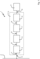
- the system 1 comprises a simplified data bus 2 (in the present embodiment an MVB), an adapter unit 3 and an evaluation unit 4.
- the adapter unit 3 comprises a coupling unit 5, a signal processing unit 6, a decoding unit 7 and an interface module 8.
- the adapter unit 3 has also has a bus input 9 and an output interface 10, which is formed by USB in the present exemplary embodiment.
- the bus input 9 is connected to the data bus 2 , as a result of which a bus signal 11 transmitted via the data bus 2 can reach the bus input 9 and thus the adapter unit 3 .
- a bus signal 11 input into the bus input 9 is input into the coupling unit 5 in which a bus signal 12 coupled over is generated from the bus signal 11 by means of a coupling capacitance (not shown here).
- the overcoupled bus signal 12 is input into the signal processing unit 6 and a processed bus signal 13 is generated there by processing the overcoupled bus signal 12 and is input into the decoding unit 7 .
- the decoding unit 7 decodes bus data encoded in the bus signal 11 and outputs the decoded bus data 14 obtained in this way to the interface module 8 .
- the interface module 8 prepares the decoded bus data 14 for output to the evaluation unit 4 via the output interface 10 .
- bus data encoded in bus signals can be output to an evaluation unit 4 without the evaluation unit 4 or the adapter unit 3 having to have an effect on the data bus 2 .
- an interface change can be made and the output interface 10 can be formed by USB (or another interface).
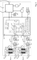
- FIG. 2 shows a more detailed representation of an embodiment of an adapter unit 3.
- the adapter unit 3 has two bus connections, which is shown in 2 marked with "Bus A” and "Bus B".
- the two buses A and B are designed as mutual redundancy.
- Each of the bus inputs 9' and 9" has two connections which enable it to be looped into the bus.
- the connection 9'.1 or 9".1 can be connected to a preceding bus user (not shown) and the connection 9'.2 or 9".2 can be connected to a following bus user (also not shown).
- Each of the connections 9'.1, 9'.2, 9".1 and 9".2 has two poles, which is indicated by two lines extending from the sketched connection. If the bus medium is formed by a twisted pair of lines, for example, one line of the bus medium can be connected to one pole and the other line of the bus medium can be connected to the other pole.
- the bus inputs 9' and 9" are each connected to a coupling unit 5' or 5", each of these coupling units 5' and 5" having a primary-side conductor structure 15' or 15" and a secondary-side conductor structure 16' or 16".
- the primary-side conductor structures 15' and 15" each have a first primary-side conductor section 17' or 17" and a second primary-side conductor section 18' or 18" and the secondary-side conductor structures 16' or 16" have a first secondary-side conductor section 19′ or 19′′ and a second conductor section 20′ or 20′′ on the secondary side.
- These conductor sections 17, 18, 19, 20 are each shown as thickened, parallel straight sections, are part of the respective conductor structure 15, 16 and form pairs a coupling capacitance, namely the first primary-side conductor section 17' or 17" with the first secondary-side conductor section 18' or 18" and the second primary-side conductor section 19' or 19" with the second secondary-side conductor section 20' or 20".
- the conductor sections 17, 18, 19, 20 can be formed by conductor tracks on a circuit board, with the conductor tracks being able to be arranged on four different levels of the circuit board.
- the overcoupled (and differentiated) bus signals 12' and 12" are input from the coupling unit 5' or 5" as differential signals into a signal processing unit 6' or 6".
- the signal processing unit 6' or 6" each includes an amplifier 21 'or 21" with variable, controlled bias and an analog-to-digital converter 22' or 22".
- the amplifier 21' or 21'' respectively amplifies the differential bus signals 12' and 12''.
- the output of the analog/digital converter 22' or 22'' is fed back to the amplifier 21' or 21'', as a result of which the bias of the amplified signal is adjusted depending on a recognized bit.
- the overcoupled bus signal 12′ or 12′′ processed in this way is input as a processed bus signal 13′ or 13′′ into an FPGA—Field Programmable Gate Array—23, in which, among other things, individual units of the adapter unit 3 are implemented.
- the processed bus signal 13' or 13" is input into a decoding unit 7' or 7".
- a function block 24' or 24'' of the decoding unit 7' or 7'' Manchester decoding, frame recognition and error handling at the bit level (in particular error recognition and possible error correction) are carried out.
- a further function block 25' or 25" of the decoding unit 7' or 7" the data frames detected in the bus signal are processed and in this way decoded bus data 14' or 14" are generated and output.
- error detection by means of CRC - Cyclic Redudancy Checking - and/or timeouts and/or filtering for errors, specific message types, senders, addressees or other criteria can be carried out.
- function block 26 the timing of the data transmissions via the two redundant data buses (Bus A, Bus B ) are made.
- the decoded bus data 14' or 14" are entered into a memory 27' or 27", which is designed as a ring memory and holds decoded bus data 14' or 14" ready for later transmission via the interface module 8 to the evaluation unit 4.
- a selection unit 28 is connected to the two memories 27' and 27" and selects the data bus (bus A, bus B) via which a received data frame of better quality was received for the decoded bus data 14' or 14" to be output , contained fewer errors, for example. If bus A and bus B are fully redundant data buses and identical bus signals are transmitted over both data buses, the selection unit 28 selects - ideally - only one set of decoded bus data from two identical copies.
- the data output by the selection unit 28 can nevertheless be regarded as "decoded bus data 14" within the meaning of the present disclosure.
- This decoded bus data 14 is transferred on the one hand to the interface module 8 for output at the output interface 10 and on the other hand to a central control logic 29 which controls functional units implemented in the FPGA 23 .
- the FPGA 23 also includes a central status logic 30, which stores status information within the FPGA 23 and optionally outputs it to a display that is not shown, for example a plurality of LEDs—light-emitting diodes.
- the FPGA 23 also includes RAM 31 - Random Access Memory - for various information, such as filter information.
- a simulation unit 32 which has a memory 33 , reproduction logic 34 , an encoder 35 (for example a Manchester encoder) and a coupling element 36 .
- Test sequences which form a basis for generating a test bus signal, are stored in memory 33, which can be in the form of RAM, for example.
- the playback logic 34 loads the required data from the memory 33 and generates bus data and an interference signal therefrom.
- the bus data are entered into the coder 35 and a bus signal is generated therefrom, which is combined with the interference signal by the coupling element 36 to form the test bus signal.
- This test bus signal is converted via a level converter 37 in such a way that the test bus signal can be further processed internally in the adapter unit as a bus signal.
- This test bus signal can, for example, be routed internally to the decoding unit 7', 7" or applied externally to the bus inputs 9' and 9" via a test adapter.
- a central clock generator 38 for outputting a system clock
- an EEPROM - Electronically Eraseable Read Only Memory - 39 for code for the FPGA 23
- an EEPROM 40 for information for the output interface 10, for example for USB meta information .
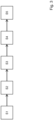
- FIG. 10 shows a flowchart with steps of an embodiment of a method according to the present disclosure.
- a bus signal 11 is first received from the data bus 2 by means of the coupling unit 5 in step S1.
- the coupling unit 5 generates an overcoupled bus signal 12 from the received bus signal 11.
- the signal processing unit 6 generates a processed bus signal 13 from the overcoupled bus signal 12.
- decoded bus data 14 are generated by the decoding unit 7 from the conditioned bus signal 13 .
- the decoded bus data 14 is output to the evaluation unit 4 via the interface module 8 .
Landscapes
- Engineering & Computer Science (AREA)
- Computer Networks & Wireless Communication (AREA)
- Signal Processing (AREA)
- Dc Digital Transmission (AREA)
- Cable Transmission Systems, Equalization Of Radio And Reduction Of Echo (AREA)
Applications Claiming Priority (1)
| Application Number | Priority Date | Filing Date | Title |
|---|---|---|---|
| DE102021128638.7A DE102021128638A1 (de) | 2021-11-03 | 2021-11-03 | Adaptereinheit und Verfahren zum Ankoppeln einer Auswerteeinheit an einen Datenbus sowie System und Fahrzeug mit entsprechender Adaptereinheit |
Publications (2)
| Publication Number | Publication Date |
|---|---|
| EP4178166A2 true EP4178166A2 (fr) | 2023-05-10 |
| EP4178166A3 EP4178166A3 (fr) | 2023-07-19 |
Family
ID=84044996
Family Applications (1)
| Application Number | Title | Priority Date | Filing Date |
|---|---|---|---|
| EP22204237.6A Withdrawn EP4178166A3 (fr) | 2021-11-03 | 2022-10-27 | Unité d'adaptateur et procédé de couplage d'une unité d'évaluation à un bus de données ainsi que système et véhicule dotés d'une unité d'adaptateur correspondante |
Country Status (2)
| Country | Link |
|---|---|
| EP (1) | EP4178166A3 (fr) |
| DE (1) | DE102021128638A1 (fr) |
Families Citing this family (1)
| Publication number | Priority date | Publication date | Assignee | Title |
|---|---|---|---|---|
| DE102023132997A1 (de) | 2023-11-27 | 2025-05-28 | Audi Aktiengesellschaft | Verfahren und Vorrichtung zur Überprüfung einer Gültigkeit einer nutzungsbegrenzten Funktion eines Kraftfahrzeugs sowie Kraftfahrzeug |
Citations (1)
| Publication number | Priority date | Publication date | Assignee | Title |
|---|---|---|---|---|
| US20090279645A1 (en) | 2005-10-06 | 2009-11-12 | Jean-Yves Berenger | Device for Reading Information on a Digital Bus Without a Wire Connection to the Network |
Family Cites Families (4)
| Publication number | Priority date | Publication date | Assignee | Title |
|---|---|---|---|---|
| DE102005051117A1 (de) | 2005-10-24 | 2007-04-26 | Hydrometer Gmbh | Kommunikations-Schnittstelle für Messgeräte |
| IL234130A (en) * | 2014-08-14 | 2017-11-30 | Orpak Systems Ltd | Device for reading vehicle data |
| JP6974194B2 (ja) * | 2018-01-25 | 2021-12-01 | 日置電機株式会社 | バス側コネクタ、装置側コネクタおよび読取システム |
| DE102018205202A1 (de) | 2018-04-06 | 2019-10-10 | Robert Bosch Gmbh | Vorrichtung zum Auskoppeln eines Signals und Verfahren zum Auskoppeln eines Signals |
-
2021
- 2021-11-03 DE DE102021128638.7A patent/DE102021128638A1/de active Pending
-
2022
- 2022-10-27 EP EP22204237.6A patent/EP4178166A3/fr not_active Withdrawn
Patent Citations (1)
| Publication number | Priority date | Publication date | Assignee | Title |
|---|---|---|---|---|
| US20090279645A1 (en) | 2005-10-06 | 2009-11-12 | Jean-Yves Berenger | Device for Reading Information on a Digital Bus Without a Wire Connection to the Network |
Also Published As
| Publication number | Publication date |
|---|---|
| DE102021128638A1 (de) | 2023-05-04 |
| EP4178166A3 (fr) | 2023-07-19 |
Similar Documents
| Publication | Publication Date | Title |
|---|---|---|
| DE19733748C2 (de) | Datenübertragungsvorrichtung | |
| EP3977682B1 (fr) | Dispositif de test de détection d'erreur pour une station d'abonné d'un système de bus série et procédé de test de mécanismes de détection d'erreur lors d'une communication dans un système de bus série | |
| EP2000866B1 (fr) | Dispositif de surveillance destiné à la reconnaissance d'un adressage incorrect d'un esclave dans un système de bus de terrain | |
| WO1998005139A1 (fr) | Procede de synchronisation de donnees, et interfaces de transmission et de reception | |
| DE112009001289T5 (de) | Kommunikationsvorrichtung, Kommunikationssystem, Kabelbaum und Kommunikationsverfahren | |
| EP2823602B1 (fr) | Dispositif de communication par bus | |
| DE102010040772A1 (de) | Dekodiereinheit und Kodiereinheit für den differentiellen Manchester-Code | |
| EP3977683B1 (fr) | Dispositif pour une station d'abonné d'un système de bus série et procédé de communication dans un système de bus série | |
| DE102011100212A1 (de) | Sende-Empfangsvorrichtung und Verfahren zum Senden und Empfangen von Daten | |
| DE102018202615A1 (de) | Teilnehmerstation für ein Bussystem und Verfahren zur Erhöhung der Datenrate eines Bussystems | |
| WO2020120555A1 (fr) | Station d'abonnés pour un système de bus série et procédé de communication dans un système de bus série | |
| EP4178166A2 (fr) | Unité d'adaptateur et procédé de couplage d'une unité d'évaluation à un bus de données ainsi que système et véhicule dotés d'une unité d'adaptateur correspondante | |
| DE102019200907A1 (de) | Teilnehmerstation für ein Bussystem und Verfahren zur Datenübertragung in einem Bussystem | |
| DE102010028485B4 (de) | Verfahren und Vorrichtung zur Absicherung von über eine Schnittstelle zu übertragenden Datenpaketen | |
| DE3888412T2 (de) | Übertragungsfilter. | |
| DE102022102195A1 (de) | Dsi3-bus mit verbesserter robustheit | |
| DE102005059012A1 (de) | ASI-Sytem zum Anschluß mehrerer Sensoren und/oder Aktuatoren an eine Steuerung | |
| EP1221220A2 (fr) | Procede et dispositif pour la communication bidirectionnelle entre au moins deux interlocuteurs | |
| EP1459488B1 (fr) | Procede et dispositif de transmission bidirectionnelle de donnees a l'alternat | |
| DE10101196A1 (de) | Interfaceschaltung und Verfahren für Digitalsignale | |
| DE102014219603B4 (de) | Stromschnittstelle zur Datenkommunikation in einem Kraftfahrzeug | |
| EP3841688B1 (fr) | Convertisseur de média et procédé de fonctionnement d'un convertisseur de média | |
| DE102013004737A1 (de) | Netzwerk und Verfahren zum Betrieb eines Netzwerks | |
| DE102022214195A1 (de) | Verfahren und Recheneinheit zur Erkennung eines unerlaubten physischen Zugriffs auf ein Bussystem | |
| DE102023001048A1 (de) | Verfahren zum Betreiben eines Verbundes von elektronischen Recheneinrichtungen in einem Kraftfahrzeug, Computerprogrammprodukt, computerlesbares Speichermedium, Verbund von elektronischen Recheneinrichtungen sowie Kraftfahrzeug |
Legal Events
| Date | Code | Title | Description |
|---|---|---|---|
| PUAI | Public reference made under article 153(3) epc to a published international application that has entered the european phase |
Free format text: ORIGINAL CODE: 0009012 |
|
| STAA | Information on the status of an ep patent application or granted ep patent |
Free format text: STATUS: THE APPLICATION HAS BEEN PUBLISHED |
|
| AK | Designated contracting states |
Kind code of ref document: A2 Designated state(s): AL AT BE BG CH CY CZ DE DK EE ES FI FR GB GR HR HU IE IS IT LI LT LU LV MC ME MK MT NL NO PL PT RO RS SE SI SK SM TR |
|
| PUAL | Search report despatched |
Free format text: ORIGINAL CODE: 0009013 |
|
| AK | Designated contracting states |
Kind code of ref document: A3 Designated state(s): AL AT BE BG CH CY CZ DE DK EE ES FI FR GB GR HR HU IE IS IT LI LT LU LV MC ME MK MT NL NO PL PT RO RS SE SI SK SM TR |
|
| RIC1 | Information provided on ipc code assigned before grant |
Ipc: B60R 16/023 20060101ALI20230609BHEP Ipc: H04L 12/40 20060101AFI20230609BHEP |
|
| STAA | Information on the status of an ep patent application or granted ep patent |
Free format text: STATUS: THE APPLICATION IS DEEMED TO BE WITHDRAWN |
|
| 18D | Application deemed to be withdrawn |
Effective date: 20240120 |