EP4184336A1 - Nicht-postierte schreibtransaktionen für einen rechnerbus - Google Patents
Nicht-postierte schreibtransaktionen für einen rechnerbus Download PDFInfo
- Publication number
- EP4184336A1 EP4184336A1 EP22202176.8A EP22202176A EP4184336A1 EP 4184336 A1 EP4184336 A1 EP 4184336A1 EP 22202176 A EP22202176 A EP 22202176A EP 4184336 A1 EP4184336 A1 EP 4184336A1
- Authority
- EP
- European Patent Office
- Prior art keywords
- work
- memory
- descriptors
- group
- accelerator
- Prior art date
- Legal status (The legal status is an assumption and is not a legal conclusion. Google has not performed a legal analysis and makes no representation as to the accuracy of the status listed.)
- Granted
Links
Images







Classifications
-
- G—PHYSICS
- G06—COMPUTING OR CALCULATING; COUNTING
- G06F—ELECTRIC DIGITAL DATA PROCESSING
- G06F13/00—Interconnection of, or transfer of information or other signals between, memories, input/output devices or central processing units
- G06F13/14—Handling requests for interconnection or transfer
- G06F13/16—Handling requests for interconnection or transfer for access to memory bus
- G06F13/1668—Details of memory controller
-
- G—PHYSICS
- G06—COMPUTING OR CALCULATING; COUNTING
- G06F—ELECTRIC DIGITAL DATA PROCESSING
- G06F13/00—Interconnection of, or transfer of information or other signals between, memories, input/output devices or central processing units
- G06F13/38—Information transfer, e.g. on bus
- G06F13/42—Bus transfer protocol, e.g. handshake; Synchronisation
- G06F13/4204—Bus transfer protocol, e.g. handshake; Synchronisation on a parallel bus
- G06F13/4221—Bus transfer protocol, e.g. handshake; Synchronisation on a parallel bus being an input/output bus, e.g. ISA bus, EISA bus, PCI bus, SCSI bus
-
- G—PHYSICS
- G06—COMPUTING OR CALCULATING; COUNTING
- G06F—ELECTRIC DIGITAL DATA PROCESSING
- G06F12/00—Accessing, addressing or allocating within memory systems or architectures
- G06F12/02—Addressing or allocation; Relocation
- G06F12/08—Addressing or allocation; Relocation in hierarchically structured memory systems, e.g. virtual memory systems
- G06F12/0802—Addressing of a memory level in which the access to the desired data or data block requires associative addressing means, e.g. caches
- G06F12/0893—Caches characterised by their organisation or structure
- G06F12/0895—Caches characterised by their organisation or structure of parts of caches, e.g. directory or tag array
-
- G—PHYSICS
- G06—COMPUTING OR CALCULATING; COUNTING
- G06F—ELECTRIC DIGITAL DATA PROCESSING
- G06F13/00—Interconnection of, or transfer of information or other signals between, memories, input/output devices or central processing units
- G06F13/14—Handling requests for interconnection or transfer
- G06F13/16—Handling requests for interconnection or transfer for access to memory bus
- G06F13/1605—Handling requests for interconnection or transfer for access to memory bus based on arbitration
- G06F13/161—Handling requests for interconnection or transfer for access to memory bus based on arbitration with latency improvement
-
- G—PHYSICS
- G06—COMPUTING OR CALCULATING; COUNTING
- G06F—ELECTRIC DIGITAL DATA PROCESSING
- G06F13/00—Interconnection of, or transfer of information or other signals between, memories, input/output devices or central processing units
- G06F13/14—Handling requests for interconnection or transfer
- G06F13/16—Handling requests for interconnection or transfer for access to memory bus
- G06F13/1605—Handling requests for interconnection or transfer for access to memory bus based on arbitration
- G06F13/1642—Handling requests for interconnection or transfer for access to memory bus based on arbitration with request queuing
-
- G—PHYSICS
- G06—COMPUTING OR CALCULATING; COUNTING
- G06F—ELECTRIC DIGITAL DATA PROCESSING
- G06F13/00—Interconnection of, or transfer of information or other signals between, memories, input/output devices or central processing units
- G06F13/14—Handling requests for interconnection or transfer
- G06F13/16—Handling requests for interconnection or transfer for access to memory bus
- G06F13/1605—Handling requests for interconnection or transfer for access to memory bus based on arbitration
- G06F13/1652—Handling requests for interconnection or transfer for access to memory bus based on arbitration in a multiprocessor architecture
-
- G—PHYSICS
- G06—COMPUTING OR CALCULATING; COUNTING
- G06F—ELECTRIC DIGITAL DATA PROCESSING
- G06F13/00—Interconnection of, or transfer of information or other signals between, memories, input/output devices or central processing units
- G06F13/14—Handling requests for interconnection or transfer
- G06F13/16—Handling requests for interconnection or transfer for access to memory bus
- G06F13/1668—Details of memory controller
- G06F13/1673—Details of memory controller using buffers
-
- G—PHYSICS
- G06—COMPUTING OR CALCULATING; COUNTING
- G06F—ELECTRIC DIGITAL DATA PROCESSING
- G06F13/00—Interconnection of, or transfer of information or other signals between, memories, input/output devices or central processing units
- G06F13/38—Information transfer, e.g. on bus
- G06F13/40—Bus structure
- G06F13/4004—Coupling between buses
- G06F13/4027—Coupling between buses using bus bridges
- G06F13/404—Coupling between buses using bus bridges with address mapping
-
- G—PHYSICS
- G06—COMPUTING OR CALCULATING; COUNTING
- G06F—ELECTRIC DIGITAL DATA PROCESSING
- G06F13/00—Interconnection of, or transfer of information or other signals between, memories, input/output devices or central processing units
- G06F13/38—Information transfer, e.g. on bus
- G06F13/42—Bus transfer protocol, e.g. handshake; Synchronisation
- G06F13/4204—Bus transfer protocol, e.g. handshake; Synchronisation on a parallel bus
- G06F13/4234—Bus transfer protocol, e.g. handshake; Synchronisation on a parallel bus being a memory bus
-
- G—PHYSICS
- G06—COMPUTING OR CALCULATING; COUNTING
- G06F—ELECTRIC DIGITAL DATA PROCESSING
- G06F13/00—Interconnection of, or transfer of information or other signals between, memories, input/output devices or central processing units
- G06F13/38—Information transfer, e.g. on bus
- G06F13/42—Bus transfer protocol, e.g. handshake; Synchronisation
- G06F13/4282—Bus transfer protocol, e.g. handshake; Synchronisation on a serial bus, e.g. I2C bus, SPI bus
-
- G—PHYSICS
- G06—COMPUTING OR CALCULATING; COUNTING
- G06F—ELECTRIC DIGITAL DATA PROCESSING
- G06F9/00—Arrangements for program control, e.g. control units
- G06F9/06—Arrangements for program control, e.g. control units using stored programs, i.e. using an internal store of processing equipment to receive or retain programs
- G06F9/30—Arrangements for executing machine instructions, e.g. instruction decode
- G06F9/30003—Arrangements for executing specific machine instructions
- G06F9/30076—Arrangements for executing specific machine instructions to perform miscellaneous control operations, e.g. NOP
-
- G—PHYSICS
- G06—COMPUTING OR CALCULATING; COUNTING
- G06F—ELECTRIC DIGITAL DATA PROCESSING
- G06F2213/00—Indexing scheme relating to interconnection of, or transfer of information or other signals between, memories, input/output devices or central processing units
- G06F2213/0026—PCI express
-
- H—ELECTRICITY
- H04—ELECTRIC COMMUNICATION TECHNIQUE
- H04L—TRANSMISSION OF DIGITAL INFORMATION, e.g. TELEGRAPHIC COMMUNICATION
- H04L47/00—Traffic control in data switching networks
- H04L47/10—Flow control; Congestion control
- H04L47/30—Flow control; Congestion control in combination with information about buffer occupancy at either end or at transit nodes
-
- H—ELECTRICITY
- H04—ELECTRIC COMMUNICATION TECHNIQUE
- H04L—TRANSMISSION OF DIGITAL INFORMATION, e.g. TELEGRAPHIC COMMUNICATION
- H04L49/00—Packet switching elements
- H04L49/30—Peripheral units, e.g. input or output ports
-
- H—ELECTRICITY
- H04—ELECTRIC COMMUNICATION TECHNIQUE
- H04L—TRANSMISSION OF DIGITAL INFORMATION, e.g. TELEGRAPHIC COMMUNICATION
- H04L49/00—Packet switching elements
- H04L49/90—Buffering arrangements
- H04L49/9047—Buffering arrangements including multiple buffers, e.g. buffer pools
-
- Y—GENERAL TAGGING OF NEW TECHNOLOGICAL DEVELOPMENTS; GENERAL TAGGING OF CROSS-SECTIONAL TECHNOLOGIES SPANNING OVER SEVERAL SECTIONS OF THE IPC; TECHNICAL SUBJECTS COVERED BY FORMER USPC CROSS-REFERENCE ART COLLECTIONS [XRACs] AND DIGESTS
- Y02—TECHNOLOGIES OR APPLICATIONS FOR MITIGATION OR ADAPTATION AGAINST CLIMATE CHANGE
- Y02D—CLIMATE CHANGE MITIGATION TECHNOLOGIES IN INFORMATION AND COMMUNICATION TECHNOLOGIES [ICT], I.E. INFORMATION AND COMMUNICATION TECHNOLOGIES AIMING AT THE REDUCTION OF THEIR OWN ENERGY USE
- Y02D10/00—Energy efficient computing, e.g. low power processors, power management or thermal management
Definitions
- CPUs Central Processing Units
- Specialized computing tasks such as graphics and image processing, are handled by graphics processors, image processors, digital signal processors, and fixed-function accelerators.
- graphics processors image processors
- digital signal processors digital signal processors
- fixed-function accelerators In today's heterogeneous machines, each type of processor is programmed in a different manner. The era of big data processing demands higher performance at lower energy as compared with today's general-purpose processors. Accelerators (either custom fixed function units or tailored programmable units, for example) are helping meet these demands.
- embodiments may be described with reference to energy conservation and energy efficiency in specific integrated circuits, such as in computing platforms or microprocessors, other embodiments are applicable to other types of integrated circuits and logic devices. Similar techniques and teachings of embodiments described herein may be applied to other types of circuits or semiconductor devices that may also benefit from better energy efficiency and energy conservation.
- the disclosed embodiments are not limited to desktop computer systems or Ultrabooks TM . And may be also used in other devices, such as handheld devices, tablets, other thin notebooks, systems on a chip (SOC) devices, and embedded applications.
- handheld devices include cellular phones, Internet protocol devices, digital cameras, personal digital assistants (PDAs), and handheld PCs.
- Embedded applications typically include a microcontroller, a digital signal processor (DSP), a system on a chip, network computers (NetPC), set-top boxes, network hubs, wide area network (WAN) switches, or any other system that can perform the functions and operations taught below.
- DSP digital signal processor
- NetPC network computers
- Set-top boxes network hubs
- WAN wide area network
- the apparatus', methods, and systems described herein are not limited to physical computing devices, but may also relate to software optimizations for energy conservation and efficiency.
- the embodiments of methods, apparatus', and systems described herein are vital to a 'green technology' future balanced with performance considerations.
- interconnect architectures to couple and communicate between the components is also increasing in complexity to ensure bandwidth requirements are met for optimal component operation.
- different market segments demand different aspects of interconnect architectures to suit the market's needs. For example, servers require higher performance, while the mobile ecosystem is sometimes able to sacrifice overall performance for power savings. Yet, it is a singular purpose of most fabrics to provide highest possible performance with maximum power saving. Below, a number of interconnects are discussed, which would potentially benefit from aspects of the disclosure described herein.
- Processor 100 includes any processor or processing device, such as a microprocessor, an embedded processor, a digital signal processor (DSP), a network processor, a handheld processor, an application processor, a co-processor, a system on a chip (SOC), or other device to execute code.
- processor 100 in one embodiment, includes at least two cores-core 101 and 102, which may include asymmetric cores or symmetric cores (the illustrated embodiment). However, processor 100 may include any number of processing elements that may be symmetric or asymmetric.
- a core often refers to logic located on an integrated circuit capable of maintaining an independent architectural state, wherein each independently maintained architectural state is associated with at least some dedicated execution resources.
- a hardware thread typically refers to any logic located on an integrated circuit capable of maintaining an independent architectural state, wherein the independently maintained architectural states share access to execution resources.
- the line between the nomenclature of a hardware thread and core overlaps.
- a core and a hardware thread are viewed by an operating system as individual logical processors, where the operating system is able to individually schedule operations on each logical processor.
- Physical processor 100 includes two cores-core 101 and 102.
- core 101 and 102 are considered symmetric cores, i.e. cores with the same configurations, functional units, and/or logic.
- core 101 includes an out-of-order processor core
- core 102 includes an in-order processor core.
- cores 101 and 102 may be individually selected from any type of core, such as a native core, a software managed core, a core adapted to execute a native Instruction Set Architecture (ISA), a core adapted to execute a translated Instruction Set Architecture (ISA), a co-designed core, or other known core.
- ISA Native Instruction Set Architecture
- ISA translated Instruction Set Architecture
- co-designed core or other known core.
- some form of translation such as a binary translation
- some form of translation such as a binary translation
- each of the architecture state registers may be referred to as processing elements, thread slots, or thread units, as described above.
- architecture state registers 101a are replicated in architecture state registers 101b, so individual architecture states/contexts are capable of being stored for logical processor 101a and logical processor 101b.
- other smaller resources such as instruction pointers and renaming logic in allocator and renamer block 130 may also be replicated for threads 101a and 101b.
- Some resources such as re-order buffers in reorder/retirement unit 135, ILTB 120, load/store buffers, and queues may be shared through partitioning.
- Other resources such as general purpose internal registers, page-table base register(s), low-level data-cache and data-TLB 115, execution unit(s) 140, and portions of out-of-order unit 135 are potentially fully shared.
- Processor 100 often includes other resources, which may be fully shared, shared through partitioning, or dedicated by/to processing elements.
- FIG. 1 an embodiment of a purely exemplary processor with illustrative logical units/resources of a processor is illustrated. Note that a processor may include, or omit, any of these functional units, as well as include any other known functional units, logic, or firmware not depicted.
- core 101 includes a simplified, representative out-of-order (OOO) processor core. But an in-order processor may be utilized in different embodiments.
- the OOO core includes a branch target buffer 120 to predict branches to be executed/taken and an instruction-translation buffer (I-TLB) 120 to store address translation entries for instructions.
- I-TLB instruction-translation buffer
- Core 101 further includes decode module 125 coupled to fetch unit 120 to decode fetched elements.
- Fetch logic in one embodiment, includes individual sequencers associated with thread slots 101a, 101b, respectively.
- core 101 is associated with a first ISA, which defines/specifies instructions executable on processor 100.
- machine code instructions that are part of the first ISA include a portion of the instruction (referred to as an opcode), which references/specifies an instruction or operation to be performed.
- Decode logic 125 includes circuitry that recognizes these instructions from their opcodes and passes the decoded instructions on in the pipeline for processing as defined by the first ISA.
- decoders 125 include logic designed or adapted to recognize specific instructions, such as transactional instruction.
- the architecture or core 101 takes specific, predefined actions to perform tasks associated with the appropriate instruction. It is important to note that any of the tasks, blocks, operations, and methods described herein may be performed in response to a single or multiple instructions; some of which may be new or old instructions.
- decoders 126 in one embodiment, recognize the same ISA (or a subset thereof). Alternatively, in a heterogeneous core environment, decoders 126 recognize a second ISA (either a subset of the first ISA or a distinct ISA).
- allocator and renamer block 130 includes an allocator to reserve resources, such as register files to store instruction processing results.
- resources such as register files to store instruction processing results.
- threads 101a and 101b are potentially capable of out-of-order execution, where allocator and renamer block 130 also reserves other resources, such as reorder buffers to track instruction results.
- Unit 130 may also include a register renamer to rename program/instruction reference registers to other registers internal to processor 100.
- Reorder/retirement unit 135 includes components, such as the reorder buffers mentioned above, load buffers, and store buffers, to support out-of-order execution and later in-order retirement of instructions executed out-of-order.
- Scheduler and execution unit(s) block 140 includes a scheduler unit to schedule instructions/operation on execution units. For example, a floating point instruction is scheduled on a port of an execution unit that has an available floating point execution unit. Register files associated with the execution units are also included to store information instruction processing results. Exemplary execution units include a floating point execution unit, an integer execution unit, a jump execution unit, a load execution unit, a store execution unit, and other known execution units.
- Lower level data cache and data translation buffer (D-TLB) 150 are coupled to execution unit(s) 140.
- the data cache is to store recently used/operated on elements, such as data operands, which are potentially held in memory coherency states.
- the D-TLB is to store recent virtual/linear to physical address translations.
- a processor may include a page table structure to break physical memory into a plurality of virtual pages.
- cores 101 and 102 share access to higher-level or further-out cache, such as a second level cache associated with on-chip interface 110.
- higher-level or further-out refers to cache levels increasing or getting further way from the execution unit(s).
- higher-level cache is a last-level data cache—last cache in the memory hierarchy on processor 100—such as a second or third level data cache.
- higher level cache is not so limited, as it may be associated with or include an instruction cache.
- a trace cache a type of instruction cache—instead may be coupled after decoder 125 to store recently decoded traces.
- an instruction potentially refers to a macro-instruction (i.e. a general instruction recognized by the decoders), which may decode into a number of micro-instructions (micro-operations).
- processor 100 also includes on-chip interface module 110.
- on-chip interface 11 is to communicate with devices external to processor 100, such as system memory 175, a chipset (often including a memory controller hub to connect to memory 175 and an I/O controller hub to connect peripheral devices), a memory controller hub, a northbridge, or other integrated circuit.
- bus 105 may include any known interconnect, such as multi-drop bus, a point-to-point interconnect, a serial interconnect, a parallel bus, a coherent (e.g. cache coherent) bus, a layered protocol architecture, a differential bus, and a GTL bus.
- Memory 175 may be dedicated to processor 100 or shared with other devices in a system. Common examples of types of memory 175 include DRAM, SRAM, non-volatile memory (NV memory), and other known storage devices. Note that device 180 may include a graphic accelerator, processor or card coupled to a memory controller hub, data storage coupled to an I/O controller hub, a wireless transceiver, a flash device, an audio controller, a network controller, or other known device.
- a memory controller hub is on the same package and/or die with processor 100.
- a portion of the core (an on-core portion) 110 includes one or more controller(s) for interfacing with other devices such as memory 175 or a graphics device 180.
- the configuration including an interconnect and controllers for interfacing with such devices is often referred to as an on-core (or un-core configuration).
- on-chip interface 110 includes a ring interconnect for on-chip communication and a high-speed serial point-to-point link 105 for off-chip communication.
- a front-end i.e. generally where syntactic processing, semantic processing, and some transformation/optimization may take place
- a back-end i.e. generally where analysis, transformations, optimizations, and code generation takes place.
- Some compilers refer to a middle, which illustrates the blurring of delineation between a front-end and back end of a compiler.
- reference to insertion, association, generation, or other operation of a compiler may take place in any of the aforementioned phases or passes, as well as any other known phases or passes of a compiler.
- a compiler potentially inserts operations, calls, functions, etc.
- compiler code or dynamic optimization code may insert such operations/calls, as well as optimize the code for execution during runtime.
- binary code (already compiled code) may be dynamically optimized during runtime.
- the program code may include the dynamic optimization code, the binary code, or a combination thereof.
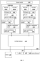
- the Device Control Register is a 64-bit BAR that contains the physical base address of device control registers. These registers provide information about device capabilities, controls to configure and enable the device, and device status.
- the size of the BARO region is dependent on the size of the Interrupt Message Storage 208. The size is 32KB plus the number of Interrupt Message Storage entries 208 times 16, rounded up to the next power of 2. For example, if the device supports 1024 Interrupt Message Storage entries 208, the Interrupt Message Storage is 16KB, and the size of BAR0 is 64KB.
- BAR2 is a 64-bit BAR that contains the physical base address of the Privileged and Non-Privileged Portals. Each portal is 64-bytes in size and is located on a separate 4KB page. This allows the portals to be independently mapped into different address spaces using CPU page tables.
- the portals are used to submit descriptors to the device.
- the Privileged Portals are used by kernel-mode software, and the Non-Privileged Portals are used by user-mode software.
- the number of Non-Privileged Portals is the same as the number of work queues supported.
- the number of Privileged Portals is Number-of-Work Queues (WQs) ⁇ (MSI-X-table-size -1).
- the address of the portal used to submit a descriptor allows the device to determine which WQ to place the descriptor in, whether the portal is privileged or non-privileged, and which MSI-X table entry may be used for the completion interrupt. For example, if the device supports 8 WQs, the WQ for a given descriptor is (Portal-address >> 12) & 0x7. If Portal-address >> 15 is 0, the portal is non-privileged; otherwise it is privileged and the MSI-X 206 table index used for the completion interrupt is Portal-address >> 15. Bits 5:0 must be 0. Bits 11:6 are ignored; thus any 64-byte-aligned address on the page can be used with the same effect.
- the number of portals in the BAR2 region is the number of WQs supported by the device times the MSI-X 206 table size.
- BAR4 is a 64-bit BAR that contains the physical base address of the Guest Portals. Each Guest Portal is 64-bytes in size and is located in a separate 4KB page. This allows the portals to be independently mapped into different address spaces using CPU extended page tables (EPT). If the Interrupt Message Storage Support field in GENCAP is 0, this BAR is not implemented.
- EPT CPU extended page tables
- MSI-X is the only PCIe interrupt capability that DSA provides and DSA does not implement legacy PCI interrupts or MSI. Details of this register structure are in the PCI Express specification.
- three PCI Express capabilities control address translation. Only certain combinations of values for these capabilities may be supported, as shown in Table 1. The values are checked at the time the Enable bit in General Control Register (GENCTRL) is set to 1. Table 1. Supported combinations of capabilities and associated values. PASID ATS PRS Operation 1 1 1 Virtual or physical addresses may be used, depending on IOMMU configuration. Addresses are translated using the PASID in the descriptor. This is the recommended mode. This mode must be used to allow user-mode access to the device or to allow sharing among multiple guests in a virtualized system. 0 1 0 Only physical addresses may be used. Addresses are translated using the BDF of the device and may be GPA or HPA, depending on IOMMU configuration.
- the device may halt and an error is reported in the Software Error Register.
- software configures the PASID capability to control whether the device uses PASID to perform address translation. If PASID is disabled, only physical addresses may be used. If PASID is enabled, virtual or physical addresses may be used, depending on IOMMU configuration. If PASID is enabled, both address translation services (ATS) and page request services (PRS) should be enabled.
- ATS address translation services
- PRS page request services
- software configures the ATS capability to control whether the device should translate addresses before performing memory accesses. If address translation is enabled in the IOMMU 2810, ATS must be enabled in the device to obtain acceptable system performance. If address translation is not enabled in the IOMMU 2810, ATS must be disabled. If ATS is disabled, only physical addresses may be used and all memory accesses are performed using Untranslated Accesses. ATS must be enabled if PASID is enabled.
- Some implementations utilize a virtual memory space that is seamlessly shared between one or more processor cores, accelerator devices, and/or other types of processing devices (e.g., I/O devices).
- one implementation utilizes a shared virtual memory (SVM) architecture in which the same virtual memory space is shared between cores, accelerator devices, and/or other processing devices.
- SVM shared virtual memory
- some implementations include heterogeneous forms of physical system memory which are addressed using a common virtual memory space. The heterogeneous forms of physical system memory may use different physical interfaces for connecting with the DSA architectures.
- an accelerator device may be directly coupled to local accelerator memory such as a high bandwidth memory (HBM) and each core may be directly coupled to a host physical memory such as a dynamic random access memory (DRAM).
- the shared virtual memory (SVM) is mapped to the combined physical memory of the HBM and DRAM so that the accelerator, processor cores, and/or other processing devices can access the HBM and DRAM using a consistent set of virtual memory addresses.
- One implementation improves the performance of accelerators with directly attached memory such as stacked DRAM or HBM, and simplifies application development for applications which make use of accelerators with directly attached memory.
- This implementation allows accelerator attached memory to be mapped as part of system memory, and accessed using Shared Virtual Memory (SVM) technology (such as that used in current IOMMU implementations), but without suffering the typical performance drawbacks associated with full system cache coherence.
- SVM Shared Virtual Memory
- the ability to access accelerator attached memory as part of system memory without onerous cache coherence overhead provides a beneficial operating environment for accelerator offload.
- the ability to access memory as part of the system address map allows host software to setup operands, and access computation results, without the overhead of traditional I/O DMA data copies. Such traditional copies involve driver calls, interrupts and memory mapped I/O (MMIO) accesses that are all inefficient relative to simple memory accesses.
- MMIO memory mapped I/O
- the ability to access accelerator attached memory without cache coherence overheads can be critical to the execution time of an offloaded computation. In cases with substantial streaming write memory traffic, for example, cache coherence overhead can cut the effective write bandwidth seen by an accelerator in half.
- the efficiency of operand setup, the efficiency of results access and the efficiency of accelerator computation all play a role in determining how well accelerator offload will work. If the cost of offloading work (e.g., setting up operands; getting results) is too high, offloading may not pay off at all, or may limit the accelerator to only very large jobs. The efficiency with which the accelerator executes a computation can have the same effect.
- One implementation applies different memory access and coherence techniques depending on the entity initiating the memory access (e.g., the accelerator, a core, etc.) and the memory being accessed (e.g., host memory or accelerator memory). These techniques are referred to generally as a "Coherence Bias" mechanism which provides for accelerator attached memory two sets of cache coherence flows, one optimized for efficient accelerator access to its attached memory, and a second optimized for host access to accelerator attached memory and shared accelerator/host access to accelerator attached memory. Further, it includes two techniques for switching between these flows, one driven by application software, and another driven by autonomous hardware hints. In both sets of coherence flows, hardware maintains full cache coherence.
- FIG. 3 is a schematic diagram of an example computer system 300 that includes an accelerator and one or more computer processor chips coupled to the processor over a multi-protocol link.
- one implementation applies to computer systems which include an accelerator 302 and one or more computer processor chips with processor cores and I/O circuitry 304, where the accelerator 302 is coupled to the processor over a multi-protocol link 314.
- the multi-protocol link 314 is a dynamically multiplexed link supporting a plurality of different protocols including, but not limited to those detailed above. It should be noted, however, that the underlying principles of the invention are not limited to any particular set of protocols.
- the accelerator 302 and Core I/O 304 may be integrated on the same semiconductor chip or different semiconductor chips, depending on the implementation.
- an accelerator memory bus 316 couples the accelerator 302 to an accelerator memory 306 and a separate host memory bus 318 couples the core I/O 304 to a host memory 308.
- the accelerator memory 306 may comprise a High Bandwidth Memory (HBM) or a stacked DRAM (some examples of which are described herein) and the host memory 308 may comprise a DRAM such as a Double-Data Rate synchronous dynamic random access memory (e.g., DDR3 SDRAM, DDR4 SDRAM, etc.).
- HBM High Bandwidth Memory
- DRAM Double-Data Rate synchronous dynamic random access memory
- both the accelerator 302 and "host” software running on the processing cores within the processor chips 304 access the accelerator memory 306 using two distinct sets of protocol flows, referred to as “Host Bias” flows and “Device Bias” flows. As described below, one implementation supports multiple options for modulating and/or choosing the protocol flows for specific memory accesses.
- the Coherence Bias flows are implemented, in part, on two protocol layers on the multi-protocol link 314 between the accelerator 302 and one of the processor chips 304: a CAC protocol layer and a MA protocol layer.
- the Coherence Bias flows are enabled by: (a) using existing opcodes in the CAC protocol in new ways, (b) the addition of new opcodes to an existing MA standard and (c) the addition of support for the MA protocol to a multi-protocol link 302 (prior links include only CAC and PCDI).
- the multi-protocol link is not limited to supporting just CAC and MA; in one implementation, it is simply required to support at least those protocols.
- the "Host Bias" flows illustrated in FIG. 3 are a set of flows that funnel all requests to accelerator memory 306 through the standard coherence controller 312 in the processor chip 304 to which the accelerator 302 is attached, including requests from the accelerator itself. This causes the accelerator 302 to take a circuitous route to access its own memory, but allows accesses from both the accelerator 302 and processor core I/O 304 to be maintained as coherent using the processor's standard coherence controllers 312.
- the flows use CAC opcodes to issues requests over the multi-protocol link to the processor's coherence controllers 312, in the same or similar manner to the way processor cores 312 issue requests to the coherence controllers 312.
- the processor chip's coherence controllers 312 may issue UPI and CAC coherence messages (e.g., snoops) that result from requests from the accelerator 302 to all peer processor core chips (e.g., 304) and internal processor agents on the accelerator's behalf, just as they would for requests from a processor core 304. In this manner, coherency is maintained between the data accessed by the accelerator 302 and processor cores I/O 304.
- UPI and CAC coherence messages e.g., snoops
- the coherence controllers 312 also conditionally issue memory access messages to the accelerator's memory controller 310 over the multi-protocol link 314. These messages are similar to the messages that the coherence controllers 312 send to the memory controllers that are local to their processor die, and include new opcodes that allow data to be returned directly to an agent internal to the accelerator 302, instead of forcing data to be returned to the processor's coherence controller 312 of the multi-protocol link 314, and then returned to the accelerator 302 as a CAC response over the multi-protocol link 314.
- All requests from processor cores 304 that target accelerator attached memory 306 are sent directly to the processors coherency controllers 312, just as they were they targeting normal host memory 308.
- the coherence controllers 312 may apply their standard cache coherence algorithms and send their standard cache coherence messages, just as they do for accesses from the accelerator 302, and just as they do for accesses to normal host memory 308.
- the coherence controllers 312 also conditionally send MA commands over the multi-protocol link 314 for this class of requests, though in this case, the MA flows return data across the multiprotocol link 314.
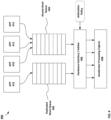
- FIG. 4 is a schematic diagram of an example work queue implementation 400 in accordance with embodiments of the present disclosure.
- Work Queues hold "descriptors" submitted by software, arbiters used to implement quality of service (QoS) and fairness policies, processing engines for processing the descriptors, an address translation and caching interface, and a memory read/write interface. Descriptors define the scope of work to be done.
- Dedicated work queues 402 store descriptors for a single application 416 while shared work queues 404 store descriptors submitted by multiple applications 410-414.
- a hardware interface/arbiter 406 dispatches descriptors from the work queues 402-404 to the accelerator processing engines 408 in accordance with a specified arbitration policy (e.g., based on the processing requirements of each application 410-416 and QoS/fairness policies).
- FIG. 4 illustrates the concept of a Shared Work Queue (SWQ), which allows multiple non-cooperating software agents (applications 410-414) to submit work through a shared work queue 404, utilizing the ENQCMD/S instructions described herein.
- SWQ Shared Work Queue
- SWQ Shared Work Queues
- VFs share a SWQ may be decided statically by the hardware design, or the mapping between a given VF's SWQ_REG to SWQ instance may be dynamically setup/torn-down through the Physical Function and its driver.
- Device designs sharing SWQ across VFs need to pay special attention to QoS and protection against denial of service attacks as described later in this section.
- care must be taken in the device design to identify which VF received an Enqueue request accepted to SWQ.
- the device When dispatching the work requests from the SWQ, the device should make sure upstream requests are properly tagged with the Requester-ID (Bus/Device/Function#) of the respective VF (in addition to the PASID that was conveyed in the Enqueue request payload).
- Requester-ID Bus/Device/Function#
- Enqueue non-posted write address Endpoint devices supporting SWQs are required to accept Enqueue non-posted writes to any addresses routed through their PF or VF memory BARs.
- the device may be required to not treat this as an error (e.g., Malformed TLP, etc.) and instead return completion with a completion status of Retry (MRS).
- MRS completion status of Retry
- SWQ queue depth and storage is device implementation specific. Device designs should ensure sufficient queue depth is supported for the SWQ to achieve maximum utilization of the device. Storage for the SWQ may be implemented on the device. Integrated devices on the SoC may utilize stolen main memory (non-OS visible private memory reserved for device use) as a spill buffer for the SWQ, allowing for larger SWQ queue-depths than possible with on-device storage. For such designs, the use of a spill buffer is transparent to software, with device hardware deciding when to spill (versus drop the Enqueue request and send a Retry completion status), fetch from the spill buffer for command execution, and maintain any command-specific ordering requirements.
- main memory non-OS visible private memory reserved for device use
- spill buffer usage is equivalent to a discrete device using local device-attached DRAM for SWQ storage.
- Device designs with a spill buffer in stolen memory must take extreme care to make sure that such stolen memory is protected from any accesses other than spill buffer read and writes by the device for which it is allocated for.
- Non-blocking SWQ behavior For performance reasons, device implementations should respond quickly to Enqueue non-posted write requests with Success or Retry completion status, and not block Enqueue completions for SWQ capacity to be freed-up to accept the request.
- the decision to accept or reject an Enqueue request to the SWQ could be based on capacity, QoS/occupancy or any other policies. Some example QoS considerations are described next.
- SWQ QoS considerations For an Enqueue non-posted write targeting a SWQ_REG address, the endpoint device may apply admission control to decide to accept the request to the respective SWQ (and send a successful completion status) or drop it (and send a Retry completion status).
- the admission control may be device and usage specific, and the specific policies supported/enforced by hardware may be exposed to software through the Physical Function (PF) driver interfaces.
- PF Physical Function
- QoS for SWQ refers only to acceptance of work requests (through enqueue requests) to the SWQ, and is orthogonal to any QoS applied by the device hardware on how QoS is applied to share the execution resources of the device when processing work requests submitted by different producers.
- PASID Provides the address space of the client that executed this instruction.
- PASID can be used for any of the type of clients (process, container, VM, etc.). It is possible for other implementation of this invention to use different identification schemes.
- ENQCMD instruction use the PASID associated with the current software thread (something the OS is expected to save/restore using XSAVES/XRSTORS instructions on thread context switches).
- ENQCMDS instruction allows the privileged software executing this instruction to specify the PASID as part of the source operand for ENQCMDS instruction.
- ENQCMDS Privilege (supervisor or user) of the client that executed this instruction. Execution of ENQCMD always indicates user permission.
- ENQCMDS allows supervisor-mode software executing it to specify either user privilege (if it is executing it on behalf of some ring-3 client), or supervisor privilege (to indicate the command is from kernel mode client) as part of the source operand for ENQCMDS instruction.
- Command Payload that is specific to the target device.
- the command payload is read from the source operand and conveyed as is by the instruction in the non-posted write payload.
- the device may use ENQCMD/S in different way. For example, some devices may treat it as a doorbell command where the payload specifies the actual work descriptor in memory to fetch from). Other devices may use the actual ENQ command to carry the device specific work descriptor, thus avoiding the latency/overhead for reading the work descriptors from main memory.
- the admission control method determines that the request cannot be accepted to the SWQ, the request is dropped and a completion is returned with a completion status of "Reject/Retry".
- the device When the work specified by the command is completed, the device generates appropriate synchronization or notification transactions to inform the client about work completions. These could be through memory writes, interrupt writes, or other methods.
- An ENQ non-posted write may be dropped by any agent (uncore, coherent fabric, I/O fabric, bridges, ...) between the CPU and the device. If any agent drops an ENQ request, such agent must return a completion response with retry status code. Software sees and treats it just like a retry response it received from the target SWQ at the device. This is possible because, ENQ ⁇ requests are self-contained and do not have any ordering constraints associated with them. System designs and fabrics may make use of this property to handle temporal congestion or back-pressure conditions in hardware/fabrics.
- FIG. 5 is a schematic diagram of an example data streaming accelerator (DSA) device comprising multiple work queues that receive descriptors submitted over an I/O fabric interface.
- FIG. 5 illustrates one implementation of a data streaming accelerator (DSA) device comprising multiple work queues 510-512 which receive descriptors submitted over an I/O fabric interface 504 (e.g., such as the multi-protocol link 314 described above).
- DSA uses the I/O fabric interface 504 for receiving downstream work requests from clients (such as processor cores, peer input/output (IO) agents (such as a network interface controller (NIC)), and/or software chained offload requests) and for upstream read, write, and address translation operations.
- clients such as processor cores, peer input/output (IO) agents (such as a network interface controller (NIC)
- NIC network interface controller
- some of the descriptors queued in the work queues 510-512 are batch descriptors 520 which contain/identify a batch of work descriptors.
- the arbiter 514 forwards batch descriptors to a batch processing unit 524 which processes batch descriptors by reading the array of descriptors 526 from memory, using addresses translated through translation cache 506 (or potentially other address translation services on the processor). Once the physical address has been identified data read/write circuit 508 reads the batch of descriptors from memory.
- the work queue configuration allows software to configure each WQ (via a WQ configuration register 502) either as a Shared Work Queue (SWQ) that receives descriptors using non-posted ENQCMD/S instructions or as a Dedicated Work Queue (DWQ) that receives descriptors using posted MOVDIR64B instructions.
- SWQ Shared Work Queue
- DWQ Dedicated Work Queue
- a DWQ may process work descriptors and batch descriptors submitted from a single application whereas a SWQ may be shared among multiple applications.
- the WQ configuration register 502 also allows software to control which WQs 510-512 feed into which accelerator engines 518 and the relative priorities of the WQs 510-512 feeding each engine.
- a descriptor may contain an operation and associated parameters (called a Work descriptor), or it can contain the address of an array of work descriptors (called a Batch descriptor).
- Software prepares the descriptor in memory and submits the descriptor to a Work Queue (WQ) 510-512 of the device.
- WQ Work Queue
- the descriptor is submitted to the device using a MOVDIR64B, ENQCMD, or ENQCMDS instruction depending on WQ's mode and client's privilege level.
- each work queue is accessible via multiple registers, each in a separate 4KB page in device MMIO space.
- One work submission register for each WQ is called “Non-privileged Portal” and is mapped into user space to be used by user-mode clients.
- Another work submission register is called “Privileged Portal” and is used by the kernel-mode driver. The rest are Guest Portals, and are used by kernel-mode clients in virtual machines.
- a DSA client uses the ENQCMD or ENQCMDS instructions to submit descriptors to the work queue.
- ENQCMD and ENQCMDS use a 64-byte non-posted write and wait for a response from the device before completing.
- the DSA returns a "success" (e.g., to the requesting client/ application) if there is space in the work queue, or a "retry” if the work queue is full.
- the ENQCMD and ENQCMDS instructions may return the status of the command submission in a zero flag (0 indicates Success, and 1 indicates Retry).
- the ENQCMD and ENQCMDS instructions may return the status of the command submission in a zero flag (0 indicates Success, and 1 indicates Retry).
- multiple clients can directly and simultaneously submit descriptors to the same work queue. Since the device provides this feedback, the clients can tell whether their descriptors were accepted.
- the ENQCMD or ENQCMDS instruction returns "success," the descriptor has been accepted by the device and queued for processing. If the instruction returns "retry,” software can either try re-submitting the descriptor to the SWQ, or if it was a user-mode client using the Non-Privileged Portal, it can request the kernel-mode driver to submit the descriptor on its behalf using the Privileged Portal. This helps avoid denial of service and provides forward progress guarantees. Alternatively, software may use other methods (e.g., using the CPU to perform the work) if the SWQ is full.
- Clients/applications are identified by the device using a 20-bit ID called process address space ID (PASID).
- the PASID is used by the device to look up addresses in the Device TLB 1722 and to send address translation or page requests to the IOMMU 1710 (e.g., over the multi-protocol link 2800).
- PASID process address space ID
- the PASID to be used with each descriptor is contained in the PASID field of the descriptor.
- ENQCMD copies the PASID of the current thread from a particular register (e.g., PASID MSR) into the descriptor while ENQCMDS allows supervisor mode software to copy the PASID into the descriptor.
- group 0 630 is comprised of two work queues 638 and 640; group 1 632 is comprised of work queue 642; work queue 2 634 is comprised of work queue 644; and group 3 636 is comprised of work queue 646.
- Engine 2 626 and engine 3 628 may be used, for example, for writing to a high bandwidth non-volatile memory such as phase-change memory.
- the bandwidth capability of these engines may be sized to match the expected write bandwidth of this type of memory.
- bits 2 and 3 of the Engine Configuration register should be set to 1, indicating that Virtual Channel 1 (VC1) should be used for traffic from these engines.
- non-volatile memory e.g., phase-change memory
- engines 2 and 3 may be unused.
- software it is possible for software to make use of them as additional low-latency paths, provided that operations submitted are tolerant of the limited bandwidth.
- Examples of multi-client accelerator / high-performance devices can include programmable GPUs, configurable offload devices, reconfigurable offload devices, fixed-function offload devices, high-performance host fabric controller devices, or high-performance I/O devices.
- DMWr Defined Memory Write Request
- AMWr Acknowledged Memory Write
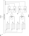
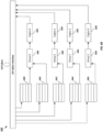
- FIGS. 7A-D are schematic diagrams illustrating an example acknowledged memory write (DMWr) request and response message flow in accordance with embodiments of the present disclosure.
- the I/O device such as the accelerator device
- the common command interface can be referred to as a shared work queue (SWQ).
- SWQ shared work queue
- the SWQ is shown as command queue 704.
- the SWQ can be a command queue 704 implemented on the accelerator device.
- the depth of the command queue 704 is implementation-specific and can be sized based on the number of outstanding commands required to feed the device to achieve its full throughput potential.
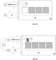
- accelerator command queue 704 is nearly full. 1) Entity A issues a command to the queue 704 via an DMWr Packet. 2) The accelerator can accept the command into the command queue. 3) The accelerator 702 can respond with a Successful Completion (SC). Note that such a device may also choose to decline packets before the queue is completely full for implementation-specific reasons (e.g., to implement TCP-like flow control mechanism).
- SC Successful Completion
- the command queue 704 is full. 4) Entity B issues command to the command queue 704 while the command queue 704 is full. 5) The accelerator 702 declines the request, and 6) the accelerator 702 sends a Completion with Request Retry Status (RRS). 7) If entity B attempts to reissue the command while the queue is still fill, the accelerator 702 can continue to send associated Completions with RRS in the status field.
- RRS Request Retry Status
- FIG. 8 is a process flow diagram 800 for performing scalable work submissions in accordance with embodiments of the present disclosure.
- an I/O device such as an accelerator
- RTS Request Retry Status
- SC Successful Completion
- a DMWr can be used to send data over PCIe.
- Deferrable Memory Writes require the Completer to return an acknowledgement to the Requester, and provides a mechanism for the recipient to defer the received data.
- the DMWr TLP facilitates use-cases that were previously not possible (or much more difficult to implement) on PCIe-based devices and links.
- DMWr provides a mechanism for Endpoints and hosts to choose to carry out or defer incoming DMWr Requests. This mechanism can be used by Endpoints and Hosts to simplify the design of flow control and fixed-length queue mechanisms.
- DMWr devices can have a single shared work queue and accept work items from multiple non-cooperating software agents in a non-blocking way.
- a DMWr can be defined as a memory write where the Requester attempts to write to a given location in Memory Space. The Completer can accept or decline this write by returning a completion with status of SC or memory request retry status (MRS), respectively (similar to the RRS above).
- MRS memory request retry status
- the Deferrable Memory Write is an Optional Non-Posted Request that enables a scalable high-performance mechanism to implement shared work queues and similar capabilities.
- DMWr Device can have a single shared work queue and accept work items from multiple non-cooperating software agents in a non-blocking way.
- DMWr Completers (a completer can be any entity that completes a non-posted write request transaction): Completers supporting DMWr Requests handle properly-formatted DMWr Requests as a Successful Completion (SC), Request Retry Status (MRS), Unsupported Request (UR), or Completer Abort (CA) for any location in its target Memory Space.
- SC Successful Completion
- MRS Request Retry Status
- UR Unsupported Request
- CA Completer Abort
- any Function in a Multi-Function Device supports DMWr Completer or DMWr routing capability, all Functions with Memory Space BARs in that device must decode properly formed DMWr Requests and handle any they do not support as an Unsupported Request (UR). Note that in such devices, Functions lacking DMWr Completer capability must not handle properly formed DMWr Requests as Malformed TLPs.
- a DMWr-aware Completer must handle a Poisoned DMWr Request as a Poisoned TLP Received error, and must also return a Completion with a Completion Status of Unsupported Request (UR). The value of the target location must remain unchanged.
- CA Completer Abort
- the Egress Port handles the Request as a DMWr Egress Blocked error and must also return a Completion with a Completion Status of UR. If the severity of the DMWr Egress Blocked error is non-fatal, then this case is handled as an Advisory Non-Fatal Error as described in the PCIe specification governing Completers sending a completion with UR/CA status.
- RC For an RC, support for peer-to-peer routing of DMWr Requests and Completions between Root Ports is optional and implementation dependent. If an RC supports DMWr routing capability between two or more Root Ports, the RC indicates that capability in each associated Root Port via the DMWr Routing Supported bit in the Device Capabilities 2 register
- An RC is not required to support DMWr routing between all pairs of Root Ports that have the DMWr Routing Supported bit Set. Software should not assume that DMWr routing is supported between all pairs of Root Ports that have the DMWr Routing Supported bit Set.
- the RC If an RC supports DMWr routing capability between two or more Root Ports, the RC indicates that capability in each associated Root Port via the DMWr Routing Supported bit in the Device Capabilities 2 register.
- a DMWr Request that is routed through a Root Port that does not support DMWr is handled as an Unsupported Request (UR).
- UR Unsupported Request
- DMWr can be used by devices and device drivers to implement control mechanisms.
- DMWr TLPs Being a Non-Posted Request, DMWr TLPs use a Completion TLP to finish the transaction. In addition, PCIe ordering rules dictate that Non-Posted TLPs cannot pass Posted TLPs, making Posted transactions preferable for improved performance. Because DMWr TLPs cannot pass Memory Read Request TLPs and DMWr TLPs can be deferred by the Completer, care is to be taken by Device and Device Driver manufacturers when attempting to read a memory location that is also the target of an outstanding DMWr Transaction.
- DMWr Transactions When DMWr Transactions are used to create a single shared work queue, care must be taken to ensure that no Requesters are denied access indefinitely to the queue due to congestion.
- Software entities that write to such a queue may choose to implement a flow control mechanism or rely on a particular programming model to ensure that all entities are able to make forward progress.
- This programming model may include a feedback mechanism or an indication to from the Function to software on the state of the queue, or a timer that delays DMWr Requests after a Completion with status MRS.
- Certain Memory Transactions can optionally have a PASID TLP Prefix containing the Process Address Space ID (PASID).
- PASID Process Address Space ID
- FIGS. 9A and 9B are visual representations of the AMWr packet.
- FIG. 9A is a schematic diagram of a 64-bit DMWr (or AMWr) packet definition 900 in accordance with embodiments of the present disclosure.
- FIG. 9B is a schematic diagram of a 32-bit DMWr (or AMWr) packet definition 920 in accordance with embodiments of the present disclosure.
- AtomicOp Completions and Read Completions I/O, Configuration, or Memory
- Completion Status [2:0] Field Value (b) Completion Status 000 Successful Completion (SC) 001 Unsupported Request (UR) 010 Configuration Request Retry Status (CRS) 100 Completer Abort (CA) 101 Memory Request Retry Status (MRS) all others Reserved
- Address-based routing rules can also facilitate the DMWr requests. Address routing is used with Memory and I/O Requests. Two address formats are specified: a 64-bit format used with a 4 DW header and a 32-bit format used with a 3 DW header. FIGS. 9A-B represent the 64 and 32 bit formats, respectively.
- Address Type (AT) field is encoded as shown in Table 10-1 Address Type (AT) Field Encodings.
- AT Address Type
- the AT field is Reserved unless explicitly stated otherwise. LN Reads and LN Writes have special requirements.
- Memory Read, Memory Write, Deferrable Memory Write, and AtomicOp Requests can use either format.
- I/O Read Requests and I/O Write Requests use the 32-bit format.
- Agents decode all address bits in the header - address aliasing is not allowed.
- the request handling rules can support DMWr. If the device supports being a target for I/O Write Requests, which are Non-Posted Requests, each associated Completion should be returned within the same time limit as for Posted Request acceptance. If the device supports being a target for Deferrable Memory Write Requests, each associated Completion is returned within the same time limit as for Posted Request acceptance.
- Flow control rules can also support DMWr.
- Each Virtual Channel has independent Flow Control.
- Flow Control distinguishes three types of TLPs:
- TLPs consume Flow Control credits as shown in Table 5 TLP Flow Control Credit Consumption. Table 5. TLP Flow Control Credit Consumption. TLP Credit Consumed Memory, I/O, Configuration Read Request 1 NPH unit Memory Write Request 1 PH + n PD units I/O, Configuration Write Request 1 NPH + 1 NPD Note: size of data written is never more than 1 (aligned) DW AtomicOp, Deferrable Memory Write Request 1 NPH + n NPD units Message Requests without data 1 PH unit Message Requests with data 1 PH + n NPD units Memory Read Completion 1 CpIH + n CpID units I/O, Configuration Read Completions 1 CpIH unit + 1 CpIH unit I/O, Configuration, Deferrable Memory Write Completions 1 CpIH unit AtomicOp Completion 1 CpIH unit + 1 CpID unit Note: size of data returned is never more than 4 (aligned) DWs
- Table 6 shows minimum advertisement for the NPD credit type. Table 6. Minimum Initial Flow Control Advertisements. Credit Type Minimum Advertisement No Scaling or Scale Factor 1 Scale Factor 4 Scale Factor 16 ... ... ... ... NPD Receiver that supports DMWr routing capability or DMWr Completer capability: 4 units - credit value of 004h Receiver that supports DMWr routing capability or DMWr Completer capability: 4 units - credit value of 004h Receiver that supports DMWr routing capability or DMWr Completer capability: 4 units-credit value of 004h Receiver that supports AtomicOp routing capability or any AtomicOp Completer capability: 2 units - credit value of 002h Receiver that supports AtomicOp routing capability or any AtomicOp Completer capability: 2 units - credit value of 002h Receiver that supports AtomicOp routing capability or any AtomicOp Completer capability: 2 units-credit value of 002h All other Receivers: 1 unit-credit value of 001h. All other Receivers: 1 unit-
- Table 7 shows a transaction layer error list.
- the transaction layer error list can be used by detecting agents, such as egress ports, to identify errors when handling DMWr packets.
- Table 7. Transaction Layer Error List. Error Name Error Type (Default Severity) Detecting Agent Action [4:0] (b) References ... ... ... ... AtomicOP Egress Blockedr ... ... ... DMWr Egress Blocked Uncorrectable (non-fatal) Egress Port: Section re: Deferred Memory Write Send ERR_COR to Root Complex. This is an Advisory Non-Fatal Error case described in Section 6.2.3.2.4.1 Completer Sending a Completion with UR/CA Status. Log the prefix/header of the DMWr Request that encountered the error. ... ... ... ... ...
- Table 8 provides bit mapping to a device capabilities 2 register: Table 8.
- Device Capabilities 2 Register Bit Location Register Description Attributes ... ... ... 27 DMWr Routing Supported -Applicable only to Switch Upstream Ports, Switch Downstream Ports, and Root Ports; must be 0b for other Function types. This bit must be set to 1b if the Port supports this optional capability.
- HWInit 28 DMWr Completer Supported -Applicable to Functions with Memory Space BARs as well as all Root Ports; This bit must be set to 1b if the function can serve as a DMWr Completer.
- Table 9 provides bit mapping to a device capabilities 4 register: Table 9.
- Device Capabilities 3 Register Bit Location Register Description Attributes 0 Deferrable Memory Write Requester Enable - Applicable only to Endpoints and Root Ports; must be hardwired to 0b for other Function types. The Function is allowed to initiate Deferrable Memory Writes only if this bit and the Bus Master Enable bit in the Command register are both Set. RW This bit is required to be RW if the Endpoint or Root Port is capable of initiating Deferrable Memory Write Requests, but otherwise is permitted to be hardwired to 0b. Default value of this bit is 0b.
- Table 10 represents definitions to uncorrectable error status register bit values.
- Table 10. Uncorrectable Error Status Register. Bit Location Register Description Attributes Default ... ... ... ... 1 DMWr Egress Blocked Status RW1CS 0b ... ... ... ...
- Table 11 represents definitions of uncorrectable error mask register bit values.
- Table 11. Uncorrectable Error Mask Register. Bit Location Register Description Attributes Default ... ... ... ... 1 DMWr Egress Blocked Mask (Optional) RWS 0b ... ... ... ... ...
- Table 12 represents definitions of uncorrectable error severity register bit values.
- Table 12. Uncorrectable Error Severity Register. Bit Location Register Description Attributes Default ... ... ... ... 1 DMWr Egress Blocked Severity (Optional) RWS 0b ... ... ... ... ...
- AMWr can be used for non-posted write requests for scability of work requests to completers.
- the following features can facilitate AMWr messaging on PCIe based interconnects:
- the Acknowledged Memory Write is a Non-Posted Request and enables easy scalability for high performance, low latency devices such as accelerators, implementing a shared work queue or an acknowledged doorbell write.
- the number of unique application clients that can submit work to such devices is typically dependent on the number of queues and doorbells supported by the device.
- accelerator-type (and other I/O) devices can have a single shared work queue and accept work items from multiple non-cooperating software agents in a non-blocking way. Devices could expose such shared work queues in an implementation-specific way.
- Root Complex supports AMWr routing capability between two or more Root Ports, the RC indicates that capability in each associated Root Port via the AMWr Routing Supported bit in the Device Capabilities 2 register
- Switch If a Switch supports AMWr routing for any of its Ports, it may do so for all of them.
- the Egress Port For a Switch or an RC, when AMWr Egress Blocking is enabled in an Egress Port, and an AMWr Request targets going out from that Egress Port, the Egress Port handles the Request as an Unsupported Request error and must also return a Completion with a Completion Status of UR.
- the Egress Port handles the Request as an AMWr Egress Blocked error and also returns a Completion with a Completion Status of UR. If the severity of the AMWr Egress Blocked error is non-fatal, this case must be handled as an Advisory Non-Fatal Error.
- An RC is not required to support AMWr routing between all pairs of Root Ports that have the AMWr Routing Supported bit Set.
- An AMWr Request that would require routing between unsupported pairs of Root Ports must be handled as an Unsupported Request (UR), and reported by the "sending" Port. If a RC supports AMWr routing capability between two or more Root Ports, it must indicate that capability in each associated Root Port via the AW Routing Supported bit in the Device Capabilities 2 register. Software must not assume that AMWr routing is supported between all pairs of Root Ports that have the AMWr Routing Supported bit Set.
- AMWr Completers (e.g., entities completing the AMWr requests) supporting AMWr Requests are required to handle properly formatted AMWr Requests as a Successful Completion (SC), Request Retry Status (RRS), Unsupported Request (UR), or Completer Abort (CA) for any location in its target Memory Space.
- SC Successful Completion
- RRS Request Retry Status
- UR Unsupported Request
- CA Completer Abort
- the Completer of an AMWr Request encounters an uncorrectable error accessing the target location or carrying out the Acknowledged Write, the Completer must handle it as a Completer Abort (CA).
- CA Completer Abort
- AMWr-aware Completers are required to handle any properly formed AMWr Requests with types or operand sizes they do not support as an Unsupported Request (UR).
- UR Unsupported Request
- any Function in a Multi-Function Device supports AMWr Completer or AMWr routing capability, all Functions with Memory Space BARs in that device can decode properly formed AMWr Requests and handle any supported functions as an Unsupported Request (UR). Note that in such devices, Functions lacking AMWr Completer capability are forbidden to handle properly formed AMWr Requests as Malformed TLPs.
- the AMWr-aware Completer is required either to carry out the Request or handle it as Completer Abort (CA) for any location in its target Memory Space.
- CA Completer Abort
- Completers are permitted to support AMWr Requests on a subset of their target Memory Space as needed by their programming model (see Section 2.3.1 Request Handling Rules).
- Memory Space structures defined or inherited by PCI Express e.g., the MSI-X Table structure) are not required to be supported as AMWr targets unless explicitly stated in the description of the structure.
- AMWr can be used by devices and device drivers to implement control mechanisms.
- AMWr TLPs Being a Non-Posted Request, AMWr TLPs uses a Completion TLP to finish the transaction.
- PCIe ordering rules state that Non-Posted TLPs cannot pass Posted TLPs, making Posted transactions preferable for improved performance.
- the packet definitions can be interpreted based, at least in part, on the following definitions, which can represent changes to the PCIe specification:
- Table 13 below is a representation of Table 2-3 of the PCIe specification.
- the Table 13 includes TLP definitions to support AMWr.
- Table 13. TLP Definitions to Support AMWr.
- TLP Type Fmt [2:0] (b) Type [4:0] (b) Description ... ... ... ... AMWr 010 011 11011 Acknowledged Memory Write Request ... ... ... ... Cpl 000 01010 Completion without Data - Used for I/O, Configuration, and Acknowledged Memory Write Completions with any Completion Status. Also used for AtomicOp Completions and Read Completions (I/O, Configuration, or Memory) with Completion Status other than Successful Completion.
- Completion Status [2:0] Field Value (b) Completion Status 000 Successful Completion (SC) 001 Unsupported Request (UR) 010 Request Retry Status (RRS) 100 Completer Abort (CA) all others Reserved
- Table 15 can provide a definition or register bits.
- Table 16 represents definitions of uncorrectable error status register bit values. Table 16. Uncorrectable Error Status Register. Bit Location Register Description Attributes Default ... ... ... ... 1 AMWr Egress Blocked Status (Optional) RW1CS 0b ... ... ... ... ...
- Table 17 represents definitions of uncorrectable error mask register bit values.
- Table 17. Uncorrectable Error Mask Register. Bit Location Register Description Attributes Default ... ... ... ... 1 AMWr Egress Blocked Mask (Optional) RWS 0b ... ... ... ... ...
- Table 18 represents definitions of uncorrectable error severity register bit values.
- Table 18. Uncorrectable Error Severity Register. Bit Location Register Description Attributes Default ... ... ... ... 1 AMWr Egress Blocked Severity (Optional) RWS 0b ... ... ... ... ...
- FIG. 10 illustrates an embodiment of a computing system including an interconnect architecture.
- System 1000 includes processor 1005 and system memory 1010 coupled to controller hub 1015.
- Processor 1005 includes any processing element, such as a microprocessor, a host processor, an embedded processor, a co-processor, or other processor.
- Processor 1005 is coupled to controller hub 1015 through front-side bus (FSB) 1006.
- FSB 1006 is a serial point-to-point interconnect as described below.
- link 1006 includes a serial, differential interconnect architecture that is compliant with different interconnect standard.
- System memory 1010 includes any memory device, such as random access memory (RAM), non-volatile (NV) memory, or other memory accessible by devices in system 1000.
- System memory 1010 is coupled to controller hub 1015 through memory interface 1016. Examples of a memory interface include a double-data rate (DDR) memory interface, a dual-channel DDR memory interface, and a dynamic RAM (DRAM) memory interface.
- DDR double-data rate
- DRAM dynamic RAM
- controller hub 1015 is a root hub, root complex, or root controller in a Peripheral Component Interconnect Express (PCIe or PCIE) interconnection hierarchy.
- controller hub 1015 include a chipset, a memory controller hub (MCH), a northbridge, an interconnect controller hub (ICH) a southbridge, and a root controller/hub.
- chipset refers to two physically separate controller hubs, i.e. a memory controller hub (MCH) coupled to an interconnect controller hub (ICH).
- MCH memory controller hub
- ICH interconnect controller hub
- current systems often include the MCH integrated with processor 1005, while controller 1015 is to communicate with I/O devices, in a similar manner as described below.
- peer-to-peer routing is optionally supported through root complex 1015.
- controller hub 1015 is coupled to switch/bridge 1020 through serial link 1019.
- Input/output modules 1017 and 1021 which may also be referred to as interfaces/ports 1017 and 1021, include/implement a layered protocol stack to provide communication between controller hub 1015 and switch 1020.
- multiple devices are capable of being coupled to switch 1020.
- Switch/bridge 1020 routes packets/messages from device 1025 upstream, i.e. up a hierarchy towards a root complex, to controller hub 1015 and downstream, i.e. down a hierarchy away from a root controller, from processor 1005 or system memory 1010 to device 1025.
- Switch 1020 in one embodiment, is referred to as a logical assembly of multiple virtual PCI-to-PCI bridge devices.
- Device 1025 includes any internal or external device or component to be coupled to an electronic system, such as an I/O device, a Network Interface Controller (NIC), an add-in card, an audio processor, a network processor, a hard-drive, a storage device, a CD/DVD ROM, a monitor, a printer, a mouse, a keyboard, a router, a portable storage device, a Firewire device, a Universal Serial Bus (USB) device, a scanner, and other input/output devices.
- NIC Network Interface Controller
- Graphics accelerator 1030 is also coupled to controller hub 1015 through serial link 1032.
- graphics accelerator 1030 is coupled to an MCH, which is coupled to an ICH.
- Switch 1020, and accordingly I/O device 1025, is then coupled to the ICH.
- I/O modules 1031 and 1018 are also to implement a layered protocol stack to communicate between graphics accelerator 1030 and controller hub 1015. Similar to the MCH discussion above, a graphics controller or the graphics accelerator 1030 itself may be integrated in processor 1005.
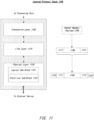
- FIG. 11 illustrates an embodiment of a interconnect architecture including a layered stack.
- Layered protocol stack 1100 includes any form of a layered communication stack, such as a Quick Path Interconnect (QPI) stack, a PCie stack, a next generation high performance computing interconnect stack, or other layered stack.
- QPI Quick Path Interconnect
- PCie stack a PCie stack
- next generation high performance computing interconnect stack or other layered stack.
- protocol stack 1100 is a PCIe protocol stack including transaction layer 1105, link layer 1110, and physical layer 1120.
- An interface such as interfaces 1017, 1018, 1021, 1022, 1026, and 1031 in Figure 1 , may be represented as communication protocol stack 1100. Representation as a communication protocol stack may also be referred to as a module or interface implementing/including a protocol stack.
- PCI Express uses packets to communicate information between components. Packets are formed in the Transaction Layer 1105 and Data Link Layer 1110 to carry the information from the transmitting component to the receiving component. As the transmitted packets flow through the other layers, they are extended with additional information necessary to handle packets at those layers. At the receiving side the reverse process occurs and packets get transformed from their Physical Layer 1120 representation to the Data Link Layer 1110 representation and finally (for Transaction Layer Packets) to the form that can be processed by the Transaction Layer 1105 of the receiving device.
- transaction layer 1105 is to provide an interface between a device's processing core and the interconnect architecture, such as data link layer 1110 and physical layer 1120.
- a primary responsibility of the transaction layer 1105 is the assembly and disassembly of packets (i.e., transaction layer packets, or TLPs).
- the translation layer 1105 typcially manages credit-base flow control for TLPs.
- PCIe implements split transactions, i.e. transactions with request and response separated by time, allowing a link to carry other traffic while the target device gathers data for the response.
- PCIe utilizes credit-based flow control.
- a device advertises an initial amount of credit for each of the receive buffers in Transaction Layer 1105.
- An external device at the opposite end of the link such as controller hub 115 in Figure 1 , counts the number of credits consumed by each TLP.
- a transaction may be transmitted if the transaction does not exceed a credit limit.
- An advantage of a credit scheme is that the latency of credit return does not affect performance, provided that the credit limit is not encountered.
- four transaction address spaces include a configuration address space, a memory address space, an input/output address space, and a message address space.
- Memory space transactions include one or more of read requests and write requests to transfer data to/from a memory-mapped location.
- memory space transactions are capable of using two different address formats, e.g., a short address format, such as a 32-bit address, or a long address format, such as 64-bit address.
- Configuration space transactions are used to access configuration space of the PCIe devices.
- Transactions to the configuration space include read requests and write requests.
- Message space transactions (or, simply messages) are defined to support in-band communication between PCIe agents.
- transaction layer 1105 assembles packet header/payload 1106. Format for current packet headers/payloads may be found in the PCIe specification at the PCIe specification website.
- FIG. 12 illustrates an embodiment of a request or packet to be generated or received within an interconnect architecture.
- An embodiment of a PCIe transaction descriptor is illustrated.
- transaction descriptor 1200 is a mechanism for carrying transaction information.
- transaction descriptor 1200 supports identification of transactions in a system.
- Other potential uses include tracking modifications of default transaction ordering and association of transaction with channels.
- Transaction descriptor 1200 includes global identifier field 1202, attributes field 1204 and channel identifier field 1206.
- global identifier field 1202 is depicted comprising local transaction identifier field 1208 and source identifier field 1210.
- global transaction identifier 1202 is unique for all outstanding requests.
- local transaction identifier field 1208 is a field generated by a requesting agent, and it is unique for all outstanding requests that require a completion for that requesting agent. Furthermore, in this example, source identifier 1210 uniquely identifies the requestor agent within a PCIe hierarchy. Accordingly, together with source ID 1210, local transaction identifier 1208 field provides global identification of a transaction within a hierarchy domain.
- Attributes field 1204 specifies characteristics and relationships of the transaction. In this regard, attributes field 1204 is potentially used to provide additional information that allows modification of the default handling of transactions.
- attributes field 1204 includes priority field 1212, reserved field 1214, ordering field 1216, and no-snoop field 1218.
- priority sub-field 1212 may be modified by an initiator to assign a priority to the transaction.
- Reserved attribute field 1214 is left reserved for future, or vendor-defined usage. Possible usage models using priority or security attributes may be implemented using the reserved attribute field.
- ordering attribute field 1216 is used to supply optional information conveying the type of ordering that may modify default ordering rules.
- an ordering attribute of "0" denotes default ordering rules are to apply, wherein an ordering attribute of "1" denotes relaxed ordering, wherein writes can pass writes in the same direction, and read completions can pass writes in the same direction.
- Snoop attribute field 1218 is utilized to determine if transactions are snooped. As shown, channel ID Field 1206 identifies a channel that a transaction is associated with.
- Link layer 1110 acts as an intermediate stage between transaction layer 1105 and the physical layer 1120.
- a responsibility of the data link layer 1110 is providing a reliable mechanism for exchanging Transaction Layer Packets (TLPs) between two components a link.
- TLPs Transaction Layer Packets
- One side of the Data Link Layer 1110 accepts TLPs assembled by the Transaction Layer 1105, applies packet sequence identifier 1111, i.e. an identification number or packet number, calculates and applies an error detection code, i.e. CRC 1112, and submits the modified TLPs to the Physical Layer 1120 for transmission across a physical to an external device.
- packet sequence identifier 1111 i.e. an identification number or packet number
- CRC 1112 error detection code
- physical layer 1120 includes logical sub block 1121 and electrical sub-block 1122 to physically transmit a packet to an external device.
- logical sub-block 1121 is responsible for the "digital" functions of Physical Layer 1121.
- the logical sub-block includes a transmit section to prepare outgoing information for transmission by physical sub-block 1122, and a receiver section to identify and prepare received information before passing it to the Link Layer 1110.
- Physical block 1122 includes a transmitter and a receiver.
- the transmitter is supplied by logical sub-block 1121 with symbols, which the transmitter serializes and transmits onto to an external device.
- the receiver is supplied with serialized symbols from an external device and transforms the received signals into a bit-stream.
- the bit-stream is de-serialized and supplied to logical sub-block 1121.
- an 8b/10b transmission code is employed, where ten-bit symbols are transmitted/received.
- special symbols are used to frame a packet with frames 1123.
- the receiver also provides a symbol clock recovered from the incoming serial stream.
- a layered protocol stack is not so limited. In fact, any layered protocol may be included/implemented.
- an port/interface that is represented as a layered protocol includes: (1) a first layer to assemble packets, i.e. a transaction layer; a second layer to sequence packets, i.e. a link layer; and a third layer to transmit the packets, i.e. a physical layer.
- CSI common standard interface
- FIG. 13 illustrates an embodiment of a transmitter and receiver pair for an interconnect architecture.
- An embodiment of a PCIe serial point to point fabric is illustrated.
- a serial point-to-point link is not so limited, as it includes any transmission path for transmitting serial data.
- a basic PCIe link includes two, low-voltage, differentially driven signal pairs: a transmit pair 1306/1311 and a receive pair 1312/1307.
- device 1305 includes transmission logic 1306 to transmit data to device 1310 and receiving logic 1307 to receive data from device 1310.
- two transmitting paths, i.e. paths 1316 and 1317, and two receiving paths, i.e. paths 1318 and 1319 are included in a PCIe link.
- a transmission path refers to any path for transmitting data, such as a transmission line, a copper line, an optical line, a wireless communication channel, an infrared communication link, or other communication path.
- a connection between two devices, such as device 1305 and device 1310, is referred to as a link, such as link 1315.
- a link may support one lane - each lane representing a set of differential signal pairs (one pair for transmission, one pair for reception).
- a link may aggregate multiple lanes denoted by xN, where N is any supported Link width, such as 1, 2, 4, 8, 12, 16, 32, 64, or wider.
- a differential pair refers to two transmission paths, such as lines 1316 and 1317, to transmit differential signals.
- lines 1316 and 1317 to transmit differential signals.
- line 1316 toggles from a low voltage level to a high voltage level, i.e. a rising edge
- line 1317 drives from a high logic level to a low logic level, i.e. a falling edge.
- Differential signals potentially demonstrate better electrical characteristics, such as better signal integrity, i.e. cross-coupling, voltage overshoot/undershoot, ringing, etc. This allows for better timing window, which enables faster transmission frequencies.
- FIG. 14 illustrates another embodiment of a block diagram for a computing system including a processor.
- a block diagram of an exemplary computer system formed with a processor that includes execution units to execute an instruction, where one or more of the interconnects implement one or more features in accordance with one embodiment of the present invention is illustrated.
- System 1400 includes a component, such as a processor 1402 to employ execution units including logic to perform algorithms for process data, in accordance with the present invention, such as in the embodiment described herein.
- System 1400 is representative of processing systems based on the PENTIUM III TM , PENTIUM 4 TM , Xeon TM , Itanium, XScale TM and/or StrongARM TM microprocessors available from Intel Corporation of Santa Clara, California, although other systems (including PCs having other microprocessors, engineering workstations, set-top boxes and the like) may also be used.
- sample system 1400 executes a version of the WINDOWS TM operating system available from Microsoft Corporation of Redmond, Washington, although other operating systems (UNIX and Linux for example), embedded software, and/or graphical user interfaces, may also be used.
- embodiments of the present invention are not limited to any specific combination of hardware circuitry and software.
- any of the aforementioned features or aspects of the invention may be utilized on one or more interconnect illustrated in FIG. 14 .
- an on-die interconnect which is not shown, for coupling internal units of processor 1402 implements one or more aspects of the invention described above.
- the invention is associated with a processor bus 1410 (e.g. Intel Quick Path Interconnect (QPI) or other known high performance computing interconnect), a high bandwidth memory path 1418 to memory 1420, a point-to-point link to graphics accelerator 1412 (e.g. a Peripheral Component Interconnect express (PCIe) compliant fabric), a controller hub interconnect 1422, an I/O or other interconnect (e.g.
- QPI Intel Quick Path Interconnect
- PCIe Peripheral Component Interconnect express
- FIG. 15 illustrates another embodiment of a block diagram for a computing system.
- SOC 1500 is included in user equipment (UE).
- UE refers to any device to be used by an end-user to communicate, such as a hand-held phone, smartphone, tablet, ultra-thin notebook, notebook with broadband adapter, or any other similar communication device.
- a UE connects to a base station or node, which potentially corresponds in nature to a mobile station (MS) in a GSM network.
- MS mobile station
- SOC 1500 includes 2 cores-1506 and 1507. Similar to the discussion above, cores 1506 and 1507 may conform to an Instruction Set Architecture, such as an Intel ® Architecture Core TM -based processor, an Advanced Micro Devices, Inc. (AMD) processor, a MIPS-based processor, an ARM-based processor design, or a customer thereof, as well as their licensees or adopters. Cores 1506 and 1507 are coupled to cache control 1508 that is associated with bus interface unit 1509 and L2 cache 1510 to communicate with other parts of system 1500. Interconnect 1510 includes an on-chip interconnect, such as an IOSF, AMBA, or other interconnect discussed above, which potentially implements one or more aspects of the described invention.
- an Intel ® Architecture Core TM -based processor such as an Intel ® Architecture Core TM -based processor, an Advanced Micro Devices, Inc. (AMD) processor, a MIPS-based processor, an ARM-based processor design, or a customer thereof, as well as their licensees or adopters.
- Interface 1510 provides communication channels to the other components, such as a Subscriber Identity Module (SIM) 1530 to interface with a SIM card, a boot rom 1535 to hold boot code for execution by cores 1506 and 1507 to initialize and boot SOC 1500, a SDRAM controller 1540 to interface with external memory (e.g. DRAM 1560), a flash controller 1545 to interface with non-volatile memory (e.g. Flash 1565), a peripheral control Q1650 (e.g. Serial Peripheral Interface) to interface with peripherals, video codecs 1520 and Video interface 1525 to display and receive input (e.g. touch enabled input), GPU 1515 to perform graphics related computations, etc. Any of these interfaces may incorporate aspects of the invention described herein.
- SIM Subscriber Identity Module
- boot rom 1535 to hold boot code for execution by cores 1506 and 1507 to initialize and boot SOC 1500
- SDRAM controller 1540 to interface with external memory (e.g. DRAM 1560)
- flash controller 1545 to interface with non
- a design may go through various stages, from creation to simulation to fabrication.
- Data representing a design may represent the design in a number of manners.
- the hardware may be represented using a hardware description language or another functional description language.
- a circuit level model with logic and/or transistor gates may be produced at some stages of the design process.
- most designs, at some stage reach a level of data representing the physical placement of various devices in the hardware model.
- the data representing the hardware model may be the data specifying the presence or absence of various features on different mask layers for masks used to produce the integrated circuit.
- the data may be stored in any form of a machine readable medium.
- a memory or a magnetic or optical storage such as a disc may be the machine readable medium to store information transmitted via optical or electrical wave modulated or otherwise generated to transmit such information.
- an electrical carrier wave indicating or carrying the code or design is transmitted, to the extent that copying, buffering, or re-transmission of the electrical signal is performed, a new copy is made.
- a communication provider or a network provider may store on a tangible, machine-readable medium, at least temporarily, an article, such as information encoded into a carrier wave, embodying techniques of embodiments of the present invention.
- a module as used herein refers to any combination of hardware, software, and/or firmware.
- a module includes hardware, such as a micro-controller, associated with a non-transitory medium to store code adapted to be executed by the micro-controller. Therefore, reference to a module, in one embodiment, refers to the hardware, which is specifically configured to recognize and/or execute the code to be held on a non-transitory medium.
- use of a module refers to the non-transitory medium including the code, which is specifically adapted to be executed by the microcontroller to perform predetermined operations.
- the term module in this example may refer to the combination of the microcontroller and the non-transitory medium.
- a first and a second module may share hardware, software, firmware, or a combination thereof, while potentially retaining some independent hardware, software, or firmware.
- use of the term logic includes hardware, such as transistors, registers, or other hardware, such as programmable logic devices.
- phrase 'to' or 'configured to,' in one embodiment refers to arranging, putting together, manufacturing, offering to sell, importing and/or designing an apparatus, hardware, logic, or element to perform a designated or determined task.
- an apparatus or element thereof that is not operating is still 'configured to' perform a designated task if it is designed, coupled, and/or interconnected to perform said designated task.
- a logic gate may provide a 0 or a 1 during operation. But a logic gate 'configured to' provide an enable signal to a clock does not include every potential logic gate that may provide a 1 or 0.
- the logic gate is one coupled in some manner that during operation the 1 or 0 output is to enable the clock.
- use of the term 'configured to' does not require operation, but instead focus on the latent state of an apparatus, hardware, and/or element, where in the latent state the apparatus, hardware, and/or element is designed to perform a particular task when the apparatus, hardware, and/or element is operating.
- use of the phrases 'capable of/to,' and or 'operable to,' in one embodiment refers to some apparatus, logic, hardware, and/or element designed in such a way to enable use of the apparatus, logic, hardware, and/or element in a specified manner.
- use of to, capable to, or operable to, in one embodiment refers to the latent state of an apparatus, logic, hardware, and/or element, where the apparatus, logic, hardware, and/or element is not operating but is designed in such a manner to enable use of an apparatus in a specified manner.
- a value includes any known representation of a number, a state, a logical state, or a binary logical state. Often, the use of logic levels, logic values, or logical values is also referred to as 1's and 0's, which simply represents binary logic states. For example, a 1 refers to a high logic level and 0 refers to a low logic level.
- a storage cell such as a transistor or flash cell, may be capable of holding a single logical value or multiple logical values.
- the decimal number ten may also be represented as a binary value of 1010 and a hexadecimal letter A. Therefore, a value includes any representation of information capable of being held in a computer system.
- states may be represented by values or portions of values.
- a first value such as a logical one
- a second value such as a logical zero
- reset and set in one embodiment, refer to a default and an updated value or state, respectively.
- a default value potentially includes a high logical value, i.e. reset
- an updated value potentially includes a low logical value, i.e. set.
- any combination of values may be utilized to represent any number of states.
- a machine-readable medium may include any mechanism for storing or transmitting information in a form readable by a machine (e.g., a computer), but is not limited to, floppy diskettes, optical disks, Compact Disc, Read-Only Memory (CD-ROMs), and magneto-optical disks, Read-Only Memory (ROMs), Random Access Memory (RAM), Erasable Programmable Read-Only Memory (EPROM), Electrically Erasable Programmable Read-Only Memory (EEPROM), magnetic or optical cards, flash memory, or a tangible, machine-readable storage used in the transmission of information over the Internet via electrical, optical, acoustical or other forms of propagated signals (e.g., carrier waves, infrared signals, digital signals, etc.). Accordingly, the computer-
- the systems, methods, and apparatuses can include one or a combination of the following examples:
Landscapes
- Engineering & Computer Science (AREA)
- Theoretical Computer Science (AREA)
- General Engineering & Computer Science (AREA)
- Physics & Mathematics (AREA)
- General Physics & Mathematics (AREA)
- Software Systems (AREA)
- Computer Hardware Design (AREA)
- Memory System Of A Hierarchy Structure (AREA)
- Retry When Errors Occur (AREA)
- Bus Control (AREA)
- Storage Device Security (AREA)
Priority Applications (1)
| Application Number | Priority Date | Filing Date | Title |
|---|---|---|---|
| EP24221978.0A EP4542961A3 (de) | 2019-04-19 | 2020-02-04 | Nicht-postierte schreibtransaktionen für einen rechnerbus |
Applications Claiming Priority (3)
| Application Number | Priority Date | Filing Date | Title |
|---|---|---|---|
| US201962836288P | 2019-04-19 | 2019-04-19 | |
| US16/566,865 US10970238B2 (en) | 2019-04-19 | 2019-09-10 | Non-posted write transactions for a computer bus |
| EP20155352.6A EP3726392B1 (de) | 2019-04-19 | 2020-02-04 | Nicht gebuchte schreibtransaktionen für einen computer-bus |
Related Parent Applications (2)
| Application Number | Title | Priority Date | Filing Date |
|---|---|---|---|
| EP20155352.6A Division EP3726392B1 (de) | 2019-04-19 | 2020-02-04 | Nicht gebuchte schreibtransaktionen für einen computer-bus |
| EP20155352.6A Division-Into EP3726392B1 (de) | 2019-04-19 | 2020-02-04 | Nicht gebuchte schreibtransaktionen für einen computer-bus |
Related Child Applications (1)
| Application Number | Title | Priority Date | Filing Date |
|---|---|---|---|
| EP24221978.0A Division EP4542961A3 (de) | 2019-04-19 | 2020-02-04 | Nicht-postierte schreibtransaktionen für einen rechnerbus |
Publications (3)
| Publication Number | Publication Date |
|---|---|
| EP4184336A1 true EP4184336A1 (de) | 2023-05-24 |
| EP4184336C0 EP4184336C0 (de) | 2024-12-25 |
| EP4184336B1 EP4184336B1 (de) | 2024-12-25 |
Family
ID=69007585
Family Applications (4)
| Application Number | Title | Priority Date | Filing Date |
|---|---|---|---|
| EP24221978.0A Pending EP4542961A3 (de) | 2019-04-19 | 2020-02-04 | Nicht-postierte schreibtransaktionen für einen rechnerbus |
| EP21152875.7A Active EP3828715B1 (de) | 2019-04-19 | 2020-02-04 | Nicht gebuchte schreibtransaktionen für einen computer-bus |
| EP20155352.6A Active EP3726392B1 (de) | 2019-04-19 | 2020-02-04 | Nicht gebuchte schreibtransaktionen für einen computer-bus |
| EP22202176.8A Active EP4184336B1 (de) | 2019-04-19 | 2020-02-04 | Nicht-postierte schreibtransaktionen für einen rechnerbus |
Family Applications Before (3)
| Application Number | Title | Priority Date | Filing Date |
|---|---|---|---|
| EP24221978.0A Pending EP4542961A3 (de) | 2019-04-19 | 2020-02-04 | Nicht-postierte schreibtransaktionen für einen rechnerbus |
| EP21152875.7A Active EP3828715B1 (de) | 2019-04-19 | 2020-02-04 | Nicht gebuchte schreibtransaktionen für einen computer-bus |
| EP20155352.6A Active EP3726392B1 (de) | 2019-04-19 | 2020-02-04 | Nicht gebuchte schreibtransaktionen für einen computer-bus |
Country Status (3)
| Country | Link |
|---|---|
| US (4) | US10970238B2 (de) |
| EP (4) | EP4542961A3 (de) |
| CN (3) | CN115481071A (de) |
Families Citing this family (40)
| Publication number | Priority date | Publication date | Assignee | Title |
|---|---|---|---|---|
| WO2018152688A1 (en) * | 2017-02-22 | 2018-08-30 | Intel Corporation | Virtualization of process address space identifiers for scalable virtualization of input/output devices |
| JP2020042879A (ja) * | 2018-09-12 | 2020-03-19 | キオクシア株式会社 | 磁気記憶装置 |
| CN114073054A (zh) | 2019-05-23 | 2022-02-18 | 慧与发展有限责任合伙企业 | 促进采用基于逐流信用的流控制的数据驱动智能网络的系统和方法 |
| KR102851375B1 (ko) | 2019-12-09 | 2025-08-26 | 삼성전자주식회사 | 스토리지 장치와 재구성 가능 로직 칩을 포함하는 스토리지 장치 세트 및 이를 포함하는 스토리지 시스템 |
| KR102787374B1 (ko) * | 2019-12-20 | 2025-03-27 | 삼성전자주식회사 | 가속기, 가속기의 동작 방법 및 가속기를 포함한 디바이스 |
| US11188471B2 (en) | 2020-04-03 | 2021-11-30 | Alibaba Group Holding Limited | Cache coherency for host-device systems |
| US12197276B2 (en) | 2020-04-29 | 2025-01-14 | Red Hat, Inc. | Memory page fault handling for network interface devices in a virtualized environment |
| US11907744B2 (en) * | 2020-06-25 | 2024-02-20 | Intel Corporation | System, apparatus and method for enabling fine-grain quality of service or rate control for work submissions |
| US11461099B2 (en) | 2020-06-25 | 2022-10-04 | Intel Corporation | System, apparatus and method for fine-grain address space selection in a processor |
| WO2022041876A1 (zh) * | 2020-08-28 | 2022-03-03 | 华为技术有限公司 | 数据传输的方法和系统 |
| US11500668B2 (en) * | 2020-10-15 | 2022-11-15 | Red Hat, Inc. | Page fault support for virtual machine network accelerators |
| US11762583B2 (en) * | 2020-10-22 | 2023-09-19 | EMC IP Holding Company, LLC | System and method for selectively throttling commands within a storage system |
| JP2022076620A (ja) * | 2020-11-10 | 2022-05-20 | キオクシア株式会社 | メモリシステムおよび制御方法 |
| US12216607B2 (en) * | 2020-11-16 | 2025-02-04 | Intel Corporation | Source ordering in device interconnects |
| US12141597B2 (en) | 2020-11-30 | 2024-11-12 | Red Hat, Inc. | Efficient out of order request completion |
| WO2022132184A1 (en) | 2020-12-20 | 2022-06-23 | Intel Corporation | System, method and apparatus for total storage encryption |
| CN112581585B (zh) * | 2020-12-24 | 2024-02-27 | 西安翔腾微电子科技有限公司 | 一种基于SysML视图的GPU命令处理模块的TLM装置及操作方法 |
| KR102568906B1 (ko) | 2021-04-13 | 2023-08-21 | 에스케이하이닉스 주식회사 | PCIe 디바이스 및 그 동작 방법 |
| KR102570943B1 (ko) * | 2021-04-13 | 2023-08-28 | 에스케이하이닉스 주식회사 | PCIe 디바이스 및 그 동작 방법 |
| KR102568909B1 (ko) | 2021-04-13 | 2023-08-21 | 에스케이하이닉스 주식회사 | PCIe 펑션 및 그 동작 방법 |
| US11928070B2 (en) | 2021-04-13 | 2024-03-12 | SK Hynix Inc. | PCIe device |
| US20220413909A1 (en) * | 2021-06-25 | 2022-12-29 | Intel Corporation | Techniques to enable quality of service control for an accelerator device |
| CN115686636A (zh) * | 2021-07-27 | 2023-02-03 | 英特尔公司 | 用于动态调整流水线深度以改善执行等待时间的方法和装置 |
| US12455701B2 (en) | 2021-07-27 | 2025-10-28 | Intel Corporation | Scalable access control checking for cross-address-space data movement |
| WO2023009641A1 (en) * | 2021-07-27 | 2023-02-02 | Intel Corporation | Data streaming accelerator |
| US12541416B2 (en) | 2021-09-23 | 2026-02-03 | Intel Corporation | Lane based normalized historical error counter view for faulty lane isolation and disambiguation of transient versus persistent errors |
| US20230100586A1 (en) * | 2021-09-24 | 2023-03-30 | Intel Corporation | Circuitry and methods for accelerating streaming data-transformation operations |
| WO2023065283A1 (en) * | 2021-10-22 | 2023-04-27 | Nokia Shanghai Bell Co., Ltd. | Ran enhancement taking into account cbs behaviour in tsc |
| KR20230082484A (ko) | 2021-12-01 | 2023-06-08 | 삼성전자주식회사 | 전자 장치의 동작 방법 |
| EP4191419B1 (de) | 2021-12-01 | 2024-09-11 | Samsung Electronics Co., Ltd. | Betriebsverfahren einer elektronischen vorrichtung |
| US12487762B2 (en) | 2022-05-10 | 2025-12-02 | Intel Corporation | Flexible provisioning of coherent memory address decoders in hardware |
| US20250103519A1 (en) * | 2022-06-14 | 2025-03-27 | Intel Corporation | Regulating command submission to a shared peripheral device |
| CN115309453B (zh) * | 2022-07-14 | 2026-05-05 | 复旦大学 | 一种支持乱序处理器数据预取的缓存访问系统 |
| US20240054011A1 (en) * | 2022-08-12 | 2024-02-15 | Intel Corporation | Data streaming accelerator |
| US20240152466A1 (en) * | 2022-11-04 | 2024-05-09 | Samsung Electronics Co., Ltd. | Systems and methods for computational acceleration |
| US20240248869A1 (en) * | 2023-01-19 | 2024-07-25 | Samsung Electronics Co., Ltd. | Method and apparatus with peripheral component interconnect express (pcie) data transmission |
| US12204941B2 (en) | 2023-05-26 | 2025-01-21 | Microsoft Technology Licensing, Llc | Preserving quality of service for client applications having workloads for execution by a compute core or a hardware accelerator |
| CN117608849A (zh) * | 2023-12-01 | 2024-02-27 | 浪潮(北京)电子信息产业有限公司 | 一种加速设备及计算加速系统 |
| CN120234170A (zh) * | 2023-12-29 | 2025-07-01 | 杭州阿里云飞天信息技术有限公司 | 一种故障处理方法、设备及存储介质 |
| US20250315399A1 (en) * | 2024-04-09 | 2025-10-09 | Sony Interactive Entertainment Inc. | Scalable messaging (networking like) endpoint for a pcie fabric based on pcie address routing |
Citations (3)
| Publication number | Priority date | Publication date | Assignee | Title |
|---|---|---|---|---|
| US20080107020A1 (en) * | 2006-11-03 | 2008-05-08 | Man Trinh | Highly-scalable hardware-based traffic management within a network processor integrated circuit |
| US20130152099A1 (en) * | 2011-12-13 | 2013-06-13 | International Business Machines Corporation | Dynamically configurable hardware queues for dispatching jobs to a plurality of hardware acceleration engines |
| US8738860B1 (en) * | 2010-10-25 | 2014-05-27 | Tilera Corporation | Computing in parallel processing environments |
Family Cites Families (24)
| Publication number | Priority date | Publication date | Assignee | Title |
|---|---|---|---|---|
| US7184399B2 (en) * | 2001-12-28 | 2007-02-27 | Intel Corporation | Method for handling completion packets with a non-successful completion status |
| US7099318B2 (en) * | 2001-12-28 | 2006-08-29 | Intel Corporation | Communicating message request transaction types between agents in a computer system using multiple message groups |
| US7340548B2 (en) * | 2003-12-17 | 2008-03-04 | Microsoft Corporation | On-chip bus |
| US7191255B2 (en) * | 2004-10-27 | 2007-03-13 | Intel Corporation | Transaction layer link down handling for PCI express |
| GB0613923D0 (en) * | 2006-07-13 | 2006-08-23 | Ibm | A method, apparatus and software for managing processing for a plurality of processors |
| US7949794B2 (en) * | 2006-11-02 | 2011-05-24 | Intel Corporation | PCI express enhancements and extensions |
| KR100810270B1 (ko) | 2006-11-07 | 2008-03-07 | 삼성전자주식회사 | 다중 입출력 통신 시스템 |
| GB2472620B (en) * | 2009-08-12 | 2016-05-18 | Cloudtran Inc | Distributed transaction processing |
| US8799550B2 (en) * | 2010-07-16 | 2014-08-05 | Advanced Micro Devices, Inc. | System and method for increased efficiency PCI express transaction |
| US9348741B1 (en) * | 2011-12-19 | 2016-05-24 | Western Digital Technologies, Inc. | Systems and methods for handling write data access requests in data storage devices |
| US9003220B2 (en) * | 2012-09-07 | 2015-04-07 | National Instruments Corporation | Switch for clock synchronization over a switched fabric |
| US9600431B2 (en) | 2012-10-22 | 2017-03-21 | Intel Corporation | High performance interconnect physical layer |
| US9749448B2 (en) * | 2014-11-25 | 2017-08-29 | Intel Corporation | Header parity error handling |
| CN105980978B (zh) * | 2014-12-13 | 2019-02-19 | 上海兆芯集成电路有限公司 | 用于检测暂停的逻辑分析器 |
| US10901940B2 (en) * | 2016-04-02 | 2021-01-26 | Intel Corporation | Processors, methods, systems, and instructions to atomically store to memory data wider than a natively supported data width |
| US9753876B1 (en) | 2016-09-22 | 2017-09-05 | International Business Machines Corporation | Processing of inbound back-to-back completions in a communication system |
| CN116755778A (zh) | 2016-12-31 | 2023-09-15 | 英特尔公司 | 用于异构计算的系统、方法和装置 |
| US10437616B2 (en) | 2016-12-31 | 2019-10-08 | Intel Corporation | Method, apparatus, system for optimized work submission to an accelerator work queue |
| US10592322B1 (en) * | 2017-06-27 | 2020-03-17 | Amazon Technologies, Inc. | Adaptive timeout mechanism |
| US10552367B2 (en) * | 2017-07-26 | 2020-02-04 | Mellanox Technologies, Ltd. | Network data transactions using posted and non-posted operations |
| US20190068466A1 (en) * | 2017-08-30 | 2019-02-28 | Intel Corporation | Technologies for auto-discovery of fault domains |
| WO2019178264A1 (en) * | 2018-03-14 | 2019-09-19 | Fungible, Inc. | Flexible processing of network packets |
| US10636577B2 (en) * | 2018-05-25 | 2020-04-28 | Qualcomm Incorporated | Safe handling of link errors in a peripheral component interconnect express (PCIE) device |
| US11593281B2 (en) * | 2019-05-08 | 2023-02-28 | Hewlett Packard Enterprise Development Lp | Device supporting ordered and unordered transaction classes |
-
2019
- 2019-09-10 US US16/566,865 patent/US10970238B2/en active Active
-
2020
- 2020-02-04 EP EP24221978.0A patent/EP4542961A3/de active Pending
- 2020-02-04 EP EP21152875.7A patent/EP3828715B1/de active Active
- 2020-02-04 EP EP20155352.6A patent/EP3726392B1/de active Active
- 2020-02-04 EP EP22202176.8A patent/EP4184336B1/de active Active
- 2020-03-18 CN CN202211327255.XA patent/CN115481071A/zh active Pending
- 2020-03-18 CN CN202110189872.7A patent/CN112882963B/zh active Active
- 2020-03-18 CN CN202010193031.9A patent/CN111831603A/zh active Pending
-
2021
- 2021-02-26 US US17/187,271 patent/US11513979B2/en active Active
-
2022
- 2022-09-28 US US17/955,353 patent/US12332813B2/en active Active
-
2025
- 2025-06-13 US US19/237,275 patent/US20250315391A1/en active Pending
Patent Citations (3)
| Publication number | Priority date | Publication date | Assignee | Title |
|---|---|---|---|---|
| US20080107020A1 (en) * | 2006-11-03 | 2008-05-08 | Man Trinh | Highly-scalable hardware-based traffic management within a network processor integrated circuit |
| US8738860B1 (en) * | 2010-10-25 | 2014-05-27 | Tilera Corporation | Computing in parallel processing environments |
| US20130152099A1 (en) * | 2011-12-13 | 2013-06-13 | International Business Machines Corporation | Dynamically configurable hardware queues for dispatching jobs to a plurality of hardware acceleration engines |
Non-Patent Citations (1)
| Title |
|---|
| ANONYMOUS: "Intel Data Streaming Accelerator Preliminary Architecture Specification", 1 November 2019 (2019-11-01), XP055692158, Retrieved from the Internet <URL:https://software.intel.com/sites/default/files/341204-intel-data-streaming-accelerator-spec.pdf> [retrieved on 20200506] * |
Also Published As
| Publication number | Publication date |
|---|---|
| US20250315391A1 (en) | 2025-10-09 |
| US20210209037A1 (en) | 2021-07-08 |
| EP3828715A3 (de) | 2021-07-28 |
| EP3828715B1 (de) | 2023-04-26 |
| US10970238B2 (en) | 2021-04-06 |
| US12332813B2 (en) | 2025-06-17 |
| US20200004703A1 (en) | 2020-01-02 |
| US11513979B2 (en) | 2022-11-29 |
| EP3828715A2 (de) | 2021-06-02 |
| EP3726392A1 (de) | 2020-10-21 |
| EP3726392B1 (de) | 2023-10-11 |
| CN111831603A (zh) | 2020-10-27 |
| EP4184336C0 (de) | 2024-12-25 |
| EP4184336B1 (de) | 2024-12-25 |
| EP4542961A3 (de) | 2025-07-09 |
| CN115481071A (zh) | 2022-12-16 |
| CN112882963A (zh) | 2021-06-01 |
| EP4542961A2 (de) | 2025-04-23 |
| US20230035420A1 (en) | 2023-02-02 |
| CN112882963B (zh) | 2025-05-13 |
Similar Documents
| Publication | Publication Date | Title |
|---|---|---|
| US12332813B2 (en) | Non-posted write transactions for a computer bus | |
| US11657015B2 (en) | Multiple uplink port devices | |
| US10437616B2 (en) | Method, apparatus, system for optimized work submission to an accelerator work queue | |
| US10191877B2 (en) | Architecture for software defined interconnect switch | |
| US11238203B2 (en) | Systems and methods for accessing storage-as-memory | |
| US20210303482A1 (en) | Sharing memory and i/o services between nodes | |
| CN108701023B (zh) | 用于带内重定时器寄存器访问的装置和系统 | |
| US9952987B2 (en) | Posted interrupt architecture | |
| US10139889B2 (en) | Method, apparatus, and system for improving resume times for root ports and root port integrated endpoints | |
| EP3629187A1 (de) | Aufzählung und verwaltung von multi-uplink-vorrichtungen | |
| US20160299860A1 (en) | Integrated component interconnect | |
| US12386772B2 (en) | Technologies for increasing link efficiency | |
| US20230013023A1 (en) | ARCHITECTURAL INTERFACES FOR GUEST SOFTWARE TO SUBMIT COMMANDS TO AN ADDRESS TRANSLATION CACHE IN XPUs | |
| EP4123466B1 (de) | Technologien zur erhöhung der effizienz einer verbindung |
Legal Events
| Date | Code | Title | Description |
|---|---|---|---|
| PUAI | Public reference made under article 153(3) epc to a published international application that has entered the european phase |
Free format text: ORIGINAL CODE: 0009012 |
|
| STAA | Information on the status of an ep patent application or granted ep patent |
Free format text: STATUS: THE APPLICATION HAS BEEN PUBLISHED |
|
| AC | Divisional application: reference to earlier application |
Ref document number: 3726392 Country of ref document: EP Kind code of ref document: P |
|
| AK | Designated contracting states |
Kind code of ref document: A1 Designated state(s): AL AT BE BG CH CY CZ DE DK EE ES FI FR GB GR HR HU IE IS IT LI LT LU LV MC MK MT NL NO PL PT RO RS SE SI SK SM TR |
|
| STAA | Information on the status of an ep patent application or granted ep patent |
Free format text: STATUS: REQUEST FOR EXAMINATION WAS MADE |
|
| 17P | Request for examination filed |
Effective date: 20231027 |
|
| RBV | Designated contracting states (corrected) |
Designated state(s): AL AT BE BG CH CY CZ DE DK EE ES FI FR GB GR HR HU IE IS IT LI LT LU LV MC MK MT NL NO PL PT RO RS SE SI SK SM TR |
|
| GRAP | Despatch of communication of intention to grant a patent |
Free format text: ORIGINAL CODE: EPIDOSNIGR1 |
|
| STAA | Information on the status of an ep patent application or granted ep patent |
Free format text: STATUS: GRANT OF PATENT IS INTENDED |
|
| RIC1 | Information provided on ipc code assigned before grant |
Ipc: H04L 49/00 20220101ALI20240702BHEP Ipc: G06F 9/30 20180101ALI20240702BHEP Ipc: H04L 49/1546 20220101ALI20240702BHEP Ipc: H04L 49/9047 20220101ALI20240702BHEP Ipc: H04L 47/6275 20220101ALI20240702BHEP Ipc: H04L 47/30 20220101ALI20240702BHEP Ipc: H04L 47/24 20220101ALI20240702BHEP Ipc: G06F 9/50 20060101ALI20240702BHEP Ipc: G06F 9/38 20180101ALI20240702BHEP Ipc: G06F 13/42 20060101ALI20240702BHEP Ipc: G06F 13/16 20060101AFI20240702BHEP |
|
| RIN1 | Information on inventor provided before grant (corrected) |
Inventor name: VAN DOREN, STEPHEN R. Inventor name: MAROLIA, PRATIK M. Inventor name: AGARWAL, ISHWAR Inventor name: VAKHARWALA, RUPIN H. Inventor name: STALLEY, SEAN O. Inventor name: HARRIMAN, DAVID J. Inventor name: SANKARAN, RAJESH M. |
|
| INTG | Intention to grant announced |
Effective date: 20240730 |
|
| GRAS | Grant fee paid |
Free format text: ORIGINAL CODE: EPIDOSNIGR3 |
|
| GRAA | (expected) grant |
Free format text: ORIGINAL CODE: 0009210 |
|
| STAA | Information on the status of an ep patent application or granted ep patent |
Free format text: STATUS: THE PATENT HAS BEEN GRANTED |
|
| AC | Divisional application: reference to earlier application |
Ref document number: 3726392 Country of ref document: EP Kind code of ref document: P |
|
| AK | Designated contracting states |
Kind code of ref document: B1 Designated state(s): AL AT BE BG CH CY CZ DE DK EE ES FI FR GB GR HR HU IE IS IT LI LT LU LV MC MK MT NL NO PL PT RO RS SE SI SK SM TR |
|
| REG | Reference to a national code |
Ref country code: GB Ref legal event code: FG4D |
|
| REG | Reference to a national code |
Ref country code: CH Ref legal event code: EP |
|
| REG | Reference to a national code |
Ref country code: DE Ref legal event code: R096 Ref document number: 602020043891 Country of ref document: DE |
|
| REG | Reference to a national code |
Ref country code: IE Ref legal event code: FG4D |
|
| U01 | Request for unitary effect filed |
Effective date: 20241225 |
|
| U07 | Unitary effect registered |
Designated state(s): AT BE BG DE DK EE FI FR IT LT LU LV MT NL PT RO SE SI Effective date: 20250108 |
|
| U20 | Renewal fee for the european patent with unitary effect paid |
Year of fee payment: 6 Effective date: 20250122 |
|
| PG25 | Lapsed in a contracting state [announced via postgrant information from national office to epo] |
Ref country code: NO Free format text: LAPSE BECAUSE OF FAILURE TO SUBMIT A TRANSLATION OF THE DESCRIPTION OR TO PAY THE FEE WITHIN THE PRESCRIBED TIME-LIMIT Effective date: 20250325 |
|
| PG25 | Lapsed in a contracting state [announced via postgrant information from national office to epo] |
Ref country code: GR Free format text: LAPSE BECAUSE OF FAILURE TO SUBMIT A TRANSLATION OF THE DESCRIPTION OR TO PAY THE FEE WITHIN THE PRESCRIBED TIME-LIMIT Effective date: 20250326 |
|
| PG25 | Lapsed in a contracting state [announced via postgrant information from national office to epo] |
Ref country code: RS Free format text: LAPSE BECAUSE OF FAILURE TO SUBMIT A TRANSLATION OF THE DESCRIPTION OR TO PAY THE FEE WITHIN THE PRESCRIBED TIME-LIMIT Effective date: 20250325 |
|
| PG25 | Lapsed in a contracting state [announced via postgrant information from national office to epo] |
Ref country code: SM Free format text: LAPSE BECAUSE OF FAILURE TO SUBMIT A TRANSLATION OF THE DESCRIPTION OR TO PAY THE FEE WITHIN THE PRESCRIBED TIME-LIMIT Effective date: 20241225 |
|
| PG25 | Lapsed in a contracting state [announced via postgrant information from national office to epo] |
Ref country code: PL Free format text: LAPSE BECAUSE OF FAILURE TO SUBMIT A TRANSLATION OF THE DESCRIPTION OR TO PAY THE FEE WITHIN THE PRESCRIBED TIME-LIMIT Effective date: 20241225 |
|
| PG25 | Lapsed in a contracting state [announced via postgrant information from national office to epo] |
Ref country code: ES Free format text: LAPSE BECAUSE OF FAILURE TO SUBMIT A TRANSLATION OF THE DESCRIPTION OR TO PAY THE FEE WITHIN THE PRESCRIBED TIME-LIMIT Effective date: 20241225 |
|
| PG25 | Lapsed in a contracting state [announced via postgrant information from national office to epo] |
Ref country code: IS Free format text: LAPSE BECAUSE OF FAILURE TO SUBMIT A TRANSLATION OF THE DESCRIPTION OR TO PAY THE FEE WITHIN THE PRESCRIBED TIME-LIMIT Effective date: 20250425 |
|
| PG25 | Lapsed in a contracting state [announced via postgrant information from national office to epo] |
Ref country code: SK Free format text: LAPSE BECAUSE OF FAILURE TO SUBMIT A TRANSLATION OF THE DESCRIPTION OR TO PAY THE FEE WITHIN THE PRESCRIBED TIME-LIMIT Effective date: 20241225 |
|
| PG25 | Lapsed in a contracting state [announced via postgrant information from national office to epo] |
Ref country code: CZ Free format text: LAPSE BECAUSE OF FAILURE TO SUBMIT A TRANSLATION OF THE DESCRIPTION OR TO PAY THE FEE WITHIN THE PRESCRIBED TIME-LIMIT Effective date: 20241225 |
|
| PG25 | Lapsed in a contracting state [announced via postgrant information from national office to epo] |
Ref country code: MC Free format text: LAPSE BECAUSE OF FAILURE TO SUBMIT A TRANSLATION OF THE DESCRIPTION OR TO PAY THE FEE WITHIN THE PRESCRIBED TIME-LIMIT Effective date: 20241225 |
|
| REG | Reference to a national code |
Ref country code: CH Ref legal event code: PL |
|
| PG25 | Lapsed in a contracting state [announced via postgrant information from national office to epo] |
Ref country code: CH Free format text: LAPSE BECAUSE OF NON-PAYMENT OF DUE FEES Effective date: 20250228 |
|
| PLBE | No opposition filed within time limit |
Free format text: ORIGINAL CODE: 0009261 |
|
| STAA | Information on the status of an ep patent application or granted ep patent |
Free format text: STATUS: NO OPPOSITION FILED WITHIN TIME LIMIT |
|
| 26N | No opposition filed |
Effective date: 20250926 |
|
| PG25 | Lapsed in a contracting state [announced via postgrant information from national office to epo] |
Ref country code: IE Free format text: LAPSE BECAUSE OF NON-PAYMENT OF DUE FEES Effective date: 20250204 |
|
| U20 | Renewal fee for the european patent with unitary effect paid |
Year of fee payment: 7 Effective date: 20260119 |
|
| PGFP | Annual fee paid to national office [announced via postgrant information from national office to epo] |
Ref country code: GB Payment date: 20260128 Year of fee payment: 7 |
|
| PG25 | Lapsed in a contracting state [announced via postgrant information from national office to epo] |
Ref country code: HR Free format text: LAPSE BECAUSE OF FAILURE TO SUBMIT A TRANSLATION OF THE DESCRIPTION OR TO PAY THE FEE WITHIN THE PRESCRIBED TIME-LIMIT Effective date: 20241225 |