EP4187585A2 - Module de puissance avec circuit d'attaque de grille intégré et composants fonctionnels dans un seul boîtier de module de puissance - Google Patents
Module de puissance avec circuit d'attaque de grille intégré et composants fonctionnels dans un seul boîtier de module de puissance Download PDFInfo
- Publication number
- EP4187585A2 EP4187585A2 EP22205806.7A EP22205806A EP4187585A2 EP 4187585 A2 EP4187585 A2 EP 4187585A2 EP 22205806 A EP22205806 A EP 22205806A EP 4187585 A2 EP4187585 A2 EP 4187585A2
- Authority
- EP
- European Patent Office
- Prior art keywords
- conductive substrate
- circuit board
- gate driver
- power
- power module
- Prior art date
- Legal status (The legal status is an assumption and is not a legal conclusion. Google has not performed a legal analysis and makes no representation as to the accuracy of the status listed.)
- Pending
Links
Images




Classifications
-
- H—ELECTRICITY
- H10—SEMICONDUCTOR DEVICES; ELECTRIC SOLID-STATE DEVICES NOT OTHERWISE PROVIDED FOR
- H10W—GENERIC PACKAGES, INTERCONNECTIONS, CONNECTORS OR OTHER CONSTRUCTIONAL DETAILS OF DEVICES COVERED BY CLASS H10
- H10W42/00—Arrangements for protection of devices
- H10W42/80—Arrangements for protection of devices protecting against overcurrent or overload, e.g. fuses or shunts
-
- H—ELECTRICITY
- H05—ELECTRIC TECHNIQUES NOT OTHERWISE PROVIDED FOR
- H05K—PRINTED CIRCUITS; CASINGS OR CONSTRUCTIONAL DETAILS OF ELECTRIC APPARATUS; MANUFACTURE OF ASSEMBLAGES OF ELECTRICAL COMPONENTS
- H05K7/00—Constructional details common to different types of electric apparatus
- H05K7/14—Mounting supporting structure in casing or on frame or rack
- H05K7/1422—Printed circuit boards receptacles, e.g. stacked structures, electronic circuit modules or box like frames
- H05K7/1427—Housings
- H05K7/1432—Housings specially adapted for power drive units or power converters
-
- H—ELECTRICITY
- H02—GENERATION; CONVERSION OR DISTRIBUTION OF ELECTRIC POWER
- H02H—EMERGENCY PROTECTIVE CIRCUIT ARRANGEMENTS
- H02H3/00—Emergency protective circuit arrangements for automatic disconnection directly responsive to an undesired change from normal electric working condition with or without subsequent reconnection ; integrated protection
- H02H3/08—Emergency protective circuit arrangements for automatic disconnection directly responsive to an undesired change from normal electric working condition with or without subsequent reconnection ; integrated protection responsive to excess current
-
- H—ELECTRICITY
- H02—GENERATION; CONVERSION OR DISTRIBUTION OF ELECTRIC POWER
- H02H—EMERGENCY PROTECTIVE CIRCUIT ARRANGEMENTS
- H02H5/00—Emergency protective circuit arrangements for automatic disconnection directly responsive to an undesired change from normal non-electric working conditions with or without subsequent reconnection
- H02H5/04—Emergency protective circuit arrangements for automatic disconnection directly responsive to an undesired change from normal non-electric working conditions with or without subsequent reconnection responsive to abnormal temperature
-
- H—ELECTRICITY
- H02—GENERATION; CONVERSION OR DISTRIBUTION OF ELECTRIC POWER
- H02H—EMERGENCY PROTECTIVE CIRCUIT ARRANGEMENTS
- H02H7/00—Emergency protective circuit arrangements specially adapted for specific types of electric machines or apparatus or for sectionalised protection of cable or line systems, and effecting automatic switching in the event of an undesired change from normal working conditions
- H02H7/10—Emergency protective circuit arrangements specially adapted for specific types of electric machines or apparatus or for sectionalised protection of cable or line systems, and effecting automatic switching in the event of an undesired change from normal working conditions for converters; for rectifiers
- H02H7/12—Emergency protective circuit arrangements specially adapted for specific types of electric machines or apparatus or for sectionalised protection of cable or line systems, and effecting automatic switching in the event of an undesired change from normal working conditions for converters; for rectifiers for static converters or rectifiers
-
- H—ELECTRICITY
- H02—GENERATION; CONVERSION OR DISTRIBUTION OF ELECTRIC POWER
- H02M—APPARATUS FOR CONVERSION BETWEEN AC AND AC, BETWEEN AC AND DC, OR BETWEEN DC AND DC, AND FOR USE WITH MAINS OR SIMILAR POWER SUPPLY SYSTEMS; CONVERSION OF DC OR AC INPUT POWER INTO SURGE OUTPUT POWER; CONTROL OR REGULATION THEREOF
- H02M1/00—Details of apparatus for conversion
- H02M1/0003—Details of control, feedback or regulation circuits
- H02M1/0006—Arrangements for supplying an adequate voltage to the control circuit of converters
-
- H—ELECTRICITY
- H02—GENERATION; CONVERSION OR DISTRIBUTION OF ELECTRIC POWER
- H02M—APPARATUS FOR CONVERSION BETWEEN AC AND AC, BETWEEN AC AND DC, OR BETWEEN DC AND DC, AND FOR USE WITH MAINS OR SIMILAR POWER SUPPLY SYSTEMS; CONVERSION OF DC OR AC INPUT POWER INTO SURGE OUTPUT POWER; CONTROL OR REGULATION THEREOF
- H02M1/00—Details of apparatus for conversion
- H02M1/08—Circuits specially adapted for the generation of control voltages for semiconductor devices incorporated in static converters
-
- H—ELECTRICITY
- H02—GENERATION; CONVERSION OR DISTRIBUTION OF ELECTRIC POWER
- H02M—APPARATUS FOR CONVERSION BETWEEN AC AND AC, BETWEEN AC AND DC, OR BETWEEN DC AND DC, AND FOR USE WITH MAINS OR SIMILAR POWER SUPPLY SYSTEMS; CONVERSION OF DC OR AC INPUT POWER INTO SURGE OUTPUT POWER; CONTROL OR REGULATION THEREOF
- H02M1/00—Details of apparatus for conversion
- H02M1/10—Arrangements incorporating converting means for enabling loads to be operated at will from different kinds of power supplies, e.g. from AC or DC
-
- H—ELECTRICITY
- H02—GENERATION; CONVERSION OR DISTRIBUTION OF ELECTRIC POWER
- H02M—APPARATUS FOR CONVERSION BETWEEN AC AND AC, BETWEEN AC AND DC, OR BETWEEN DC AND DC, AND FOR USE WITH MAINS OR SIMILAR POWER SUPPLY SYSTEMS; CONVERSION OF DC OR AC INPUT POWER INTO SURGE OUTPUT POWER; CONTROL OR REGULATION THEREOF
- H02M1/00—Details of apparatus for conversion
- H02M1/32—Means for protecting converters other than automatic disconnection
-
- H—ELECTRICITY
- H02—GENERATION; CONVERSION OR DISTRIBUTION OF ELECTRIC POWER
- H02M—APPARATUS FOR CONVERSION BETWEEN AC AND AC, BETWEEN AC AND DC, OR BETWEEN DC AND DC, AND FOR USE WITH MAINS OR SIMILAR POWER SUPPLY SYSTEMS; CONVERSION OF DC OR AC INPUT POWER INTO SURGE OUTPUT POWER; CONTROL OR REGULATION THEREOF
- H02M1/00—Details of apparatus for conversion
- H02M1/32—Means for protecting converters other than automatic disconnection
- H02M1/327—Means for protecting converters other than automatic disconnection against abnormal temperatures
-
- H—ELECTRICITY
- H03—ELECTRONIC CIRCUITRY
- H03K—PULSE TECHNIQUE
- H03K17/00—Electronic switching or gating, i.e. not by contact-making and –breaking
- H03K17/51—Electronic switching or gating, i.e. not by contact-making and –breaking characterised by the components used
- H03K17/56—Electronic switching or gating, i.e. not by contact-making and –breaking characterised by the components used by the use, as active elements, of semiconductor devices
- H03K17/567—Circuits characterised by the use of more than one type of semiconductor device, e.g. BIMOS, composite devices such as IGBT
-
- H—ELECTRICITY
- H05—ELECTRIC TECHNIQUES NOT OTHERWISE PROVIDED FOR
- H05K—PRINTED CIRCUITS; CASINGS OR CONSTRUCTIONAL DETAILS OF ELECTRIC APPARATUS; MANUFACTURE OF ASSEMBLAGES OF ELECTRICAL COMPONENTS
- H05K5/00—Casings, cabinets or drawers for electric apparatus
- H05K5/0026—Casings, cabinets or drawers for electric apparatus provided with connectors and printed circuit boards [PCB], e.g. automotive electronic control units
-
- H—ELECTRICITY
- H10—SEMICONDUCTOR DEVICES; ELECTRIC SOLID-STATE DEVICES NOT OTHERWISE PROVIDED FOR
- H10W—GENERIC PACKAGES, INTERCONNECTIONS, CONNECTORS OR OTHER CONSTRUCTIONAL DETAILS OF DEVICES COVERED BY CLASS H10
- H10W42/00—Arrangements for protection of devices
-
- H—ELECTRICITY
- H10—SEMICONDUCTOR DEVICES; ELECTRIC SOLID-STATE DEVICES NOT OTHERWISE PROVIDED FOR
- H10W—GENERIC PACKAGES, INTERCONNECTIONS, CONNECTORS OR OTHER CONSTRUCTIONAL DETAILS OF DEVICES COVERED BY CLASS H10
- H10W70/00—Package substrates; Interposers; Redistribution layers [RDL]
- H10W70/60—Insulating or insulated package substrates; Interposers; Redistribution layers
- H10W70/62—Insulating or insulated package substrates; Interposers; Redistribution layers characterised by their interconnections
- H10W70/65—Shapes or dispositions of interconnections
- H10W70/658—Shapes or dispositions of interconnections for devices provided for in groups H10D8/00 - H10D48/00
-
- H—ELECTRICITY
- H10—SEMICONDUCTOR DEVICES; ELECTRIC SOLID-STATE DEVICES NOT OTHERWISE PROVIDED FOR
- H10W—GENERIC PACKAGES, INTERCONNECTIONS, CONNECTORS OR OTHER CONSTRUCTIONAL DETAILS OF DEVICES COVERED BY CLASS H10
- H10W70/00—Package substrates; Interposers; Redistribution layers [RDL]
- H10W70/60—Insulating or insulated package substrates; Interposers; Redistribution layers
- H10W70/67—Insulating or insulated package substrates; Interposers; Redistribution layers characterised by their insulating layers or insulating parts
- H10W70/68—Shapes or dispositions thereof
- H10W70/6875—Shapes or dispositions thereof being on a metallic substrate, e.g. insulated metal substrates [IMS]
-
- H—ELECTRICITY
- H10—SEMICONDUCTOR DEVICES; ELECTRIC SOLID-STATE DEVICES NOT OTHERWISE PROVIDED FOR
- H10W—GENERIC PACKAGES, INTERCONNECTIONS, CONNECTORS OR OTHER CONSTRUCTIONAL DETAILS OF DEVICES COVERED BY CLASS H10
- H10W72/00—Interconnections or connectors in packages
- H10W72/50—Bond wires
-
- H—ELECTRICITY
- H10—SEMICONDUCTOR DEVICES; ELECTRIC SOLID-STATE DEVICES NOT OTHERWISE PROVIDED FOR
- H10W—GENERIC PACKAGES, INTERCONNECTIONS, CONNECTORS OR OTHER CONSTRUCTIONAL DETAILS OF DEVICES COVERED BY CLASS H10
- H10W74/00—Encapsulations, e.g. protective coatings
- H10W74/40—Encapsulations, e.g. protective coatings characterised by their materials
-
- H—ELECTRICITY
- H10—SEMICONDUCTOR DEVICES; ELECTRIC SOLID-STATE DEVICES NOT OTHERWISE PROVIDED FOR
- H10W—GENERIC PACKAGES, INTERCONNECTIONS, CONNECTORS OR OTHER CONSTRUCTIONAL DETAILS OF DEVICES COVERED BY CLASS H10
- H10W76/00—Containers; Fillings or auxiliary members therefor; Seals
- H10W76/10—Containers or parts thereof
- H10W76/12—Containers or parts thereof characterised by their shape
-
- H—ELECTRICITY
- H10—SEMICONDUCTOR DEVICES; ELECTRIC SOLID-STATE DEVICES NOT OTHERWISE PROVIDED FOR
- H10W—GENERIC PACKAGES, INTERCONNECTIONS, CONNECTORS OR OTHER CONSTRUCTIONAL DETAILS OF DEVICES COVERED BY CLASS H10
- H10W76/00—Containers; Fillings or auxiliary members therefor; Seals
- H10W76/10—Containers or parts thereof
- H10W76/12—Containers or parts thereof characterised by their shape
- H10W76/13—Containers comprising a conductive base serving as an interconnection
-
- H—ELECTRICITY
- H10—SEMICONDUCTOR DEVICES; ELECTRIC SOLID-STATE DEVICES NOT OTHERWISE PROVIDED FOR
- H10W—GENERIC PACKAGES, INTERCONNECTIONS, CONNECTORS OR OTHER CONSTRUCTIONAL DETAILS OF DEVICES COVERED BY CLASS H10
- H10W90/00—Package configurations
-
- H—ELECTRICITY
- H02—GENERATION; CONVERSION OR DISTRIBUTION OF ELECTRIC POWER
- H02M—APPARATUS FOR CONVERSION BETWEEN AC AND AC, BETWEEN AC AND DC, OR BETWEEN DC AND DC, AND FOR USE WITH MAINS OR SIMILAR POWER SUPPLY SYSTEMS; CONVERSION OF DC OR AC INPUT POWER INTO SURGE OUTPUT POWER; CONTROL OR REGULATION THEREOF
- H02M1/00—Details of apparatus for conversion
- H02M1/0003—Details of control, feedback or regulation circuits
- H02M1/0009—Devices or circuits for detecting current in a converter
-
- H—ELECTRICITY
- H02—GENERATION; CONVERSION OR DISTRIBUTION OF ELECTRIC POWER
- H02M—APPARATUS FOR CONVERSION BETWEEN AC AND AC, BETWEEN AC AND DC, OR BETWEEN DC AND DC, AND FOR USE WITH MAINS OR SIMILAR POWER SUPPLY SYSTEMS; CONVERSION OF DC OR AC INPUT POWER INTO SURGE OUTPUT POWER; CONTROL OR REGULATION THEREOF
- H02M7/00—Conversion of AC power input into DC power output; Conversion of DC power input into AC power output
- H02M7/003—Constructional details, e.g. physical layout, assembly, wiring or busbar connections
-
- H—ELECTRICITY
- H02—GENERATION; CONVERSION OR DISTRIBUTION OF ELECTRIC POWER
- H02M—APPARATUS FOR CONVERSION BETWEEN AC AND AC, BETWEEN AC AND DC, OR BETWEEN DC AND DC, AND FOR USE WITH MAINS OR SIMILAR POWER SUPPLY SYSTEMS; CONVERSION OF DC OR AC INPUT POWER INTO SURGE OUTPUT POWER; CONTROL OR REGULATION THEREOF
- H02M7/00—Conversion of AC power input into DC power output; Conversion of DC power input into AC power output
- H02M7/66—Conversion of AC power input into DC power output; Conversion of DC power input into AC power output with possibility of reversal
-
- H—ELECTRICITY
- H10—SEMICONDUCTOR DEVICES; ELECTRIC SOLID-STATE DEVICES NOT OTHERWISE PROVIDED FOR
- H10W—GENERIC PACKAGES, INTERCONNECTIONS, CONNECTORS OR OTHER CONSTRUCTIONAL DETAILS OF DEVICES COVERED BY CLASS H10
- H10W40/00—Arrangements for thermal protection or thermal control
- H10W40/20—Arrangements for cooling
- H10W40/25—Arrangements for cooling characterised by their materials
- H10W40/255—Arrangements for cooling characterised by their materials having a laminate or multilayered structure, e.g. direct bond copper [DBC] ceramic substrates
-
- H—ELECTRICITY
- H10—SEMICONDUCTOR DEVICES; ELECTRIC SOLID-STATE DEVICES NOT OTHERWISE PROVIDED FOR
- H10W—GENERIC PACKAGES, INTERCONNECTIONS, CONNECTORS OR OTHER CONSTRUCTIONAL DETAILS OF DEVICES COVERED BY CLASS H10
- H10W70/00—Package substrates; Interposers; Redistribution layers [RDL]
- H10W70/60—Insulating or insulated package substrates; Interposers; Redistribution layers
- H10W70/611—Insulating or insulated package substrates; Interposers; Redistribution layers for connecting multiple chips together
-
- H—ELECTRICITY
- H10—SEMICONDUCTOR DEVICES; ELECTRIC SOLID-STATE DEVICES NOT OTHERWISE PROVIDED FOR
- H10W—GENERIC PACKAGES, INTERCONNECTIONS, CONNECTORS OR OTHER CONSTRUCTIONAL DETAILS OF DEVICES COVERED BY CLASS H10
- H10W90/00—Package configurations
- H10W90/401—Package configurations characterised by multiple insulating or insulated package substrates, interposers or RDLs
-
- H—ELECTRICITY
- H10—SEMICONDUCTOR DEVICES; ELECTRIC SOLID-STATE DEVICES NOT OTHERWISE PROVIDED FOR
- H10W—GENERIC PACKAGES, INTERCONNECTIONS, CONNECTORS OR OTHER CONSTRUCTIONAL DETAILS OF DEVICES COVERED BY CLASS H10
- H10W90/00—Package configurations
- H10W90/701—Package configurations characterised by the relative positions of pads or connectors relative to package parts
Definitions
- the present disclosure relates to the field of power modules, power devices, and gate drivers.
- IPMs Present day intelligent power modules
- logic components such as one or more gate drivers
- various power devices inside a single housing
- IPMs including both logic components, such as one or more gate drivers, and various power devices inside a single housing
- Industrial power modules which are used in various industrial applications such as for frequency conversion, for power conversion equipment such as uninterruptable power supplies, industrial motor drives, embedded motor drives, AC-DC power supplies, etc. are typically driven by an external gate driver that is housed outside of housing of the power module.
- the gate driver and any additional logic components are typically placed outside of the power module due to the fact that power devices require improved insulation compared to present day IPMs.
- Such external placements require a lot of space, which could be saved if the logic components necessary to control the power module were integrated into the housing of the power module. Accordingly, it would be beneficial to enable IPMs for industrial applications, for example, to provide industrial IPMs.
- an apparatus comprising a power module housing.
- the power module housing includes a conductive substrate and a circuit board positioned overlying the conductive substrate.
- the power module housing includes an insulation material electrically insulating the conductive substrate from the circuit board.
- the power module housing includes a gate driver mounted to the circuit board.
- the power module housing includes at least one power device mounted to the conductive substrate and is controlled by the gate driver.
- the power module includes a monitoring component mounted at least to the conductive substrate and is operatively coupled to the gate driver and the power device.
- an apparatus comprising a power module housing.
- the power module housing includes a conductive substrate and a circuit board positioned adjacent to the conductive substrate.
- the power module housing includes an insulation material electrically insulating the conductive substrate from the circuit board.
- the power module housing includes a gate driver mounted to the circuit board.
- the power module housing includes a power device mounted to the conductive substrate and is controlled by the gate driver.
- the power module includes a monitoring component mounted at least to the conductive substrate and is operatively coupled to the gate driver and the power device.
- an apparatus comprising a power module housing.
- the power module housing includes a conductive substrate and a circuit board separate from the conductive substrate.
- the power module housing includes an insulation material electrically insulating the conductive substrate from the circuit board.
- the power module housing includes a gate driver mounted to the circuit board.
- the power module housing includes a power device mounted to the conductive substrate and is controlled by the gate driver.
- the power module includes a monitoring component mounted to the conductive substrate and is operatively coupled to the gate driver and the switch.
- a power module that integrates a gate driver and additional monitoring components into a single power module housing of the power module.
- power modules do not provide this level of integration within a single power module housing.
- a power module may merely include power semiconductors such as switches, insulated-gate bipolar transistors (IGBTs), metal-oxide-semiconductor field-effect transitions (MOSFETs), etc.
- a gate driver that controls these power semiconductors is located external to the power module housing.
- the gate driver may be mounted to a circuit board that is within an external housing that is separate and external to the power module housing. Additional monitoring components are also housed external to the power module housing of the power module.
- monitoring components may relate to overcurrent protection devices, temperature protection devices, current measurement devices, voltage measurement devices, and/or other protection features. Because the monitoring components are external to the power module housing, additional connection pins are required. These additional connection pins must be placed as close as possible to the power semiconductors due to magnetic coupling. The additional connection pins and the additional external housings for the gate driver and monitoring components increases cost, size, and complexity.
- a gate driver such as a galvanically isolated gate driver, power devices such as power switches or thyristors driven by the gate driver, and monitoring components are integrated together within the same power module housing.
- the gate driver may be mounted to a circuit board within the power module housing.
- the power devices, and monitoring components may be mounted to a conductive substrate (e.g., integrated into the conductive substrate at a chip level).
- the conductive substrate may comprise a direct copper bonded board (DCB board) or an integrated metal substrate (IMS) board.
- DCB board direct copper bonded board
- IMS integrated metal substrate
- the power module housing may comprise an insulation material, which may comprise a potting gel such as silicone gel, an insulative soft potting material, etc.
- the insulation material electrically insulates the conductive substrate from the circuit board in order to mitigate interference from inductances, couplings, cross talk, or other issues that can occur due to the relatively high operating voltage of the conductive substrate.
- the conductive substrate may operate at voltages between about 1.2kV and 5kV or any other voltage.
- the circuit board and components mounted to the circuit board may operate at a much lower voltage such as between about 3.3V and 5V.
- the circuit board and components mounted to the circuit board would be damaged by the high voltage of the conductive substrate. Such damage is mitigated by separating the conductive substrate and the circuit board, and by electrically insulating the conductive substrate and the circuit board using the insulation material.
- monitoring components may be integrated into the power module housing with the gate driver. These monitoring components may at least be integrated into the conductive substrate and may provide various functions such as overcurrent protection and/or over-temperature protection at a chip level, current measurement, voltage measurement, temperature measurement, and/or other functionality.
- the ability to integrate the monitoring components, power devices and the gate driver into a single power module housing of a power module reduces the overall size, complexity, and cost because such components are not housed external to the power module housing.
- the size of the power module housing may be kept relatively small because the insulation material allows for both the circuit board and the conductive substrate to be located within the power module housing within close proximity to one another without interference from inductances, couplings, cross talk, or other issues.
- the power module housing may measure between 30 mm x 30 mm to 100 mm x 100mm. Additionally, the use of the insulation material ensures that the high operating voltage of the conductive substrate and components on the conductive substrate do not damage the circuit board and components on the circuit board that operate at a much lower voltage.
- Fig. 1 illustrates a cross-sectional view of a power module housing 100.
- the power module housing 100 includes a conductive substrate 104.
- the conductive substrate 104 comprises a conductive material, such as copper.
- the conductive substrate 104 comprises a direct copper bonded (DCB) board or an insulated metal substrate (IMS) board.
- DCB direct copper bonded
- IMS insulated metal substrate
- the conductive substrate 104 may be located on one side of the power module housing 100, such as a bottom side of the power module housing 100. It may be appreciated that the conductive substrate 104 may be located anywhere inside the power module housing 100.
- the power module housing 100 includes a circuit board 112.
- the circuit board 112 is positioned separate from the conductive substrate 104 such that the circuit board 112 does not directly touch the conductive substrate 104.
- the circuit board 112 is located overlaying (e.g., above) but not touching the conductive substrate 104.
- the circuit board 112 and the conductive substrate 104 are both located within the power module housing 100 but are separated from one another because the circuit board 112 and the conductive substrate 104 operate at different voltages that could otherwise cause damage.
- the conductive substrate 104 may operate at a relatively high voltage such as between about 1.2kV and about 5kV or any other voltage that is higher than a voltage of the circuit board 112 that operates at voltages between about 3.3V and 5V or any other voltage.
- the higher voltage of the conductive substrate 104 can damage the circuit board 112, and thus the conductive substrate 104 is positioned separate from the circuit board 112.
- an insulation material 136 may be included within the power module housing 100.
- the insulation material 136 may partially fill an inside cavity of the power module housing 100.
- the insulation material 136 may completely fill the inside cavity of the power module housing 100.
- the insulation material 136 comprises a potting gel, such as a silicone material, a silicone gel material, an insulation potting material, or any other insulation material.
- the distance between the circuit board 112 and the conductive substrate 104 may be relatively short, such as 3 mm, due to the electric insulation provided by the insulation material 136.
- the temperature of the conductive substrate 104 may increase.
- the temperature increase of the conductive substrate 104 may lead to an increase of the temperature of the circuit board 112, which may cause the temperature of the circuit board 112 to reach or exceed a junction temperature of the components mounted on the circuit board 112.
- the distance between the circuit board 112 and the conductive substrate 104 may be wider to avoid thermal coupling.
- the distance necessary for electrical insulation between the circuit board 112 and the conductive substrate 104 may be 3 mm while the distance necessary for thermal insulation may be 5 mm. Consequently, the distance between the circuit board 112 and the conductive substrate 104 may be 5 mm.
- the distance between the circuit board 112 and the conductive substrate 104 is chosen to satisfy both electrical and thermal requirements.
- one or more devices may be mounted to the circuit board 112. These devices may operate within a voltage range supported by the circuit board 112 such as between about 3.3V to about 5V or some other voltage achieved using various voltage modification components.
- a gate driver 114 may be mounted to the circuit board 112.
- the gate driver 114 may comprise a galvanically isolated gate driver or other type of gate driver.
- the gate driver 114 may be controlled by an external controller 118 that is located external to (outside) the power module housing 100.
- the external controller 118 may connect to the gate driver 114 through a circuit board connector 116 that provides communication from the circuit board 112 to components located external to the power module housing 100 such as the external controller 118.
- the external controller 118 may be configured to generate pulse width modulation signals used to control the gate driver 114. These pulse width modulation signals may be transmitted from the external controller 118 through the circuit board connector 116 and the circuit board 112 to the gate driver 114.
- the gate driver 114 may be operatively coupled to and configured to control the gate of one or more power devices mounted to (e.g., integrated within at a chip level) the conductive substrate 104, such as a power device 110 and/or other power semiconductors not illustrated.
- the power device 110 may comprise a switch or a thyristor mounted to or integrated within the conductive substrate 104.
- the gate driver 114 may control a gate of the power device 110, for example, in order to open or close a switch or to change a mode of a thyristor.
- a conductive connector 130 connects the gate driver 114 to the power device 110, and the insulation material 136 is formed around the conductive connector 130 and otherwise electrically insulates the gate driver 114 from the power device 110.
- conductive connectors 120 - 134 may be used to provide connectivity between components within the power module housing 100 and connectivity outside the power module housing 100.
- conductive connector 132 and conductive connector 134 are connected to the conductive substrate 104 and extend through the power module housing 100 to outside the power module housing 100.
- External components may be connected to the conductive connector 132 and conductive connector 134 so that the external components can communicate (e.g., send and receive electrical signals) with components mounted to or integrated within the conductive substrate 104.
- Conductive connector 120 connects at least a part of a first monitoring component 106 to the circuit board 112.
- Conductive connector 126 connects at least a part of a second monitoring component 108 to the circuit board 112.
- Conductive connector 122, conductive connector 124, and conductive connector 128 connect the conductive substrate 104 to the circuit board 112 so that components mounted to the circuit board 112 can communicate (e.g., send and receive electrical signals) with the components mounted to or integrated within the conductive substrate 104.
- the insulation material 136 may be formed around the conductive connectors 120 - 134 and between the circuit board 112 and the conductive substrate 104.
- the conductive connectors 120 - 134 may comprise a conductive material, such as copper.
- the conductive connectors 120 - 134 comprise press-fit pins.
- a press-fit pin, such as the conductive connector 130 comprises press-fit section 131 and a contact hole 133.
- the press-fit section 131 includes at least one of the following CuFeP; CuZr; CuCrZr; CuMg; CuCrTiSi; CuCrAgFeTiSi; and CuNiSiMg.
- the contact hole 133 may be part of or connected to the conductive substrate 104.
- the press-fit section 131 is pressed into the contact hole 133 so that the press-fit section 131 is plastically deformed, and one end of the press-fit section 131 both mechanically and electrically contacts the conductive substrate 104 such as to form a connection with the power device 110.
- the other end of the press-fit section 131 is electrically connected to the circuit board 112 such as to form a connection with the gate driver 114.
- the gate driver 114 is operatively (electrically) connected to the power device 110 by the conductive connector 130 (the press fit pin).
- bond wires may be used to form electrical connections instead of the conductive connectors 120 - 134.
- the bond wires may connect to the conductive substrate 104 and then extend up and around the circuit board 112 in order to connect on top of the circuit board 112.
- a length of the circuit board 112 may be shorter than a length of the conductive substrate 104 so that the bond wires can go up and around the edges of the circuit board 112.
- one or more monitoring components may be mounted at least to (e.g., integrated within such as at a chip level) the conductive substrate 104, such as the first monitoring component 106, the second monitoring component 108, and/or other monitoring components not illustrated.
- a monitoring component may be operatively coupled to the gate driver 114, the power device 110, other power semiconductors integrated within the conductive substrate 104, other monitoring components integrated within the conductive substrate 104, the circuit board 112, or other components mounted to the circuit board 112.
- the monitoring components, the conductive substrate 104, the circuit board 112, and the gate driver 114 are all integrated and housed within the same single power module housing 100.
- the insulation material 136 is used to mitigate interference from inductances, couplings, cross talk, or other issues due to the relatively higher operating voltage of the conductive substrate 104 and components mounted to (integrated within) the conductive substrate 104 (e.g., 1.2kV and 5kV or any other voltage) compared to the relatively lower operating voltage (e.g., 3.3V to 5V) of the circuit board 112, the gate driver 114, and/or other components mounted to the circuit board 112. Electrical insulation provided by the insulation material 136 enables the ability to integrate current measurement functionality, voltage measurement functionality, temperature measurement functionality, an internal power supply, over-temperature protection, overcurrent protection, a rectifier, and/or other functionality of monitoring components into the power module housing 100.
- the power module housing comprises an internal power supply mounted to the conductive substrate 104 that provides power to one or more monitoring components, power devices, and/or other components mounted on (integrated within) the conductive substrate 104.
- the internal power supply provides power to the gate driver mounted on the circuit board 112 and in particular provides a voltage that the gate driver requires to control a gate of the power device 110, which may, for example, be 15 V in some embodiments.
- a monitoring component comprises a current measurement device used to measure current values associated with one more power devices, and/or other components mounted on (integrated within) the conductive substrate 104.
- the current measurement device may be used by a component mounted to the circuit board 112 in order to obtain current measurements within the conductive substrate 104.
- the current measurement device may comprise an integrated current mirror (a current sense).
- a monitoring component comprises a voltage measurement device used to measure voltage values associated with one more monitoring components, switches, power semiconductors, and/or other components mounted on (integrated within) the conductive substrate 104.
- the voltage measurement device may be used by a component mounted to the circuit board 112 in order to obtain voltage measurements within the conductive substrate 104.
- a monitoring component comprises a temperature measurement device (e.g., a temperature dependent diode or resistor on chip within the conductive substrate 104) used to measure temperature values associated with one more power devices, and/or other components mounted on (integrated within) the conductive substrate 104.
- a temperature measurement device e.g., a temperature dependent diode or resistor on chip within the conductive substrate 104 used to measure temperature values associated with one more power devices, and/or other components mounted on (integrated within) the conductive substrate 104.
- a monitoring component comprises an overcurrent protection device used to switch off one or more power devices, and/or other components mounted on (integrated within) the conductive substrate 104 based upon a current measurement exceeding a threshold value. In this way, the overcurrent protection device may provide current protection at a chip level.
- a monitoring component comprises a temperature protection device used to switch off one or more power devices, and/or other components mounted on (integrated within) the conductive substrate 104 based upon a temperature measurement exceeding a threshold value. In this way, the temperature protection device may provide over-temperature protection at a chip level.
- the temperature protection device, the overcurrent protection device, and/or other protective circuits may be suitable for IGBTs and/or MOSFETs, and may include integrated current mirror (a current sense) or integrated temperature measurement (e.g., a temperature dependent diode or resistor on chip or in the conductive substrate 104).
- integrated current mirror a current sense
- integrated temperature measurement e.g., a temperature dependent diode or resistor on chip or in the conductive substrate 104.
- the circuit board 112 and the conductive substrate 104 may be positioned within the power module housing 100 according to various configurations. In some embodiments, the circuit board 112 may be positioned adjacent the conductive substrate 104, as illustrated by Fig. 2 .
- the insulation material 136 is formed between the circuit board 112 and the conductive substrate 104 to provide electrical insulation between the circuit board 112 and the conductive substrate 104.
- one or more bond wires are used. For example, a first bond wire 202 may be connected between the conductive substrate 104 and the circuit board 112. A second bond wire 204 may be connected between the power device 110 and the circuit board 112.
- the bond wires may comprise a cooper material.
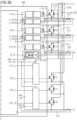
- Fig. 3 illustrates a system overview showing various components that may be integrated into the power module housing 100.
- Fig. 3 is split into two parts Fig. 3A and Fig. 3B .
- the power module housing 100 includes a control circuit 308, which may be mounted to the circuit board 112.
- control circuit 308 is a six-channel gate driver.
- the control circuit 308 may include six single channel gate drivers or three dual-channel gate drivers or any combination thereof.
- the at least one power device is part of a plurality of power devices 312 implementing a controlled three phase rectifier 302 that operates based upon control signals CTRL_R, CRTL_S, and CRTL_T.
- the monitoring components comprise voltage measurement devices 304, which may be configured to measure various voltages within the power module housing 100 such VTN, VSN, VRN, and VDC.
- the power module housing comprises an internal power supply 306 that may provide power to the control circuit 308 and to various components within the power module housing 100.
- the monitoring components comprise current measurement components 314, such as shunts to measure AC current.
- the monitoring components comprise an overcurrent detection device 316. These monitoring components may be mounted to (integrated within) the conductive substrate 104 and may be connected to the control circuit 308.
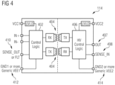
- Fig. 4 illustrates an example of the gate driver 114.
- the gate driver 114 may comprise control logic 402 on an input side of the gate driver 114.
- the gate driver 114 may comprise high voltage (HV) control logic 406 at an output side of the gate driver 114, which provides control signals to the power device 110 via the OUT pin 407.
- the gate driver 114 comprises transmission and receiver elements 404, which may be combined into a single transceiver setup. Transmission between the input side and the output side of the gate driver 114 through the transmission and receiver elements 404 can be capacitive or inductive through a coreless transformer.
- the gate driver 114 may comprise a sense out pin 410 or FLT, which depends on whether the gate driver 114 actually conveys a signal representing a sense parameter or determines that a fault condition is present.
- the gate driver 114 may comprise a sense input pin 408 that may be coupled to components mounted at least to (integrated within) the conductive substrate 104, such as monitoring components.
- the gate driver 114 may comprise a ground 412 on the input side and a ground 414 on the output side.
- a monitoring component may be configured to provide a signal indicative of a parameter of a power device (e.g., a measured current parameter, a measured temperature parameter, etc.) to the gate driver 114 through the sense input pin 408.
- the signal is processed by the control logic 402, which may perform an operation based upon the signal such as an operation to turn off the power device based upon the parameter of the power device (e.g., a measured current parameter exceeding a threshold, a measured temperature parameter exceeding a threshold, etc.).
- the monitoring component may provide the signal indicative of the parameter of the power device to the gate driver 114 through the sense input pin 408.
- the gate driver 114 may provide the signal to an external controller, such as through the sense output 410.
- Fig. 5A illustrates an example of the gate driver 114 connected to various monitoring components that are mounted to (integrated within) the conductive substrate 104, such as a first monitoring component 502, a second monitoring component 504, a third monitoring component 506, and/or a fourth monitoring component 508 that may provide safety features.
- the first monitoring component 502 utilizes current sense functionality (e.g., current sense resistance) to determine whether to shut down a gate current in response to a measured current exceeding a threshold. In this way, the first monitoring component 502 provides overcurrent protection.
- the third monitoring component 506 is similar to the first monitoring component 506 except that the third monitoring component 506 has further includes a diode 523 arranged inside the power device. A forward voltage of the diode 523 is temperature dependent, and is measured by the gate driver 114, thereby enabling temperature monitoring in addition to current monitoring.
- first monitoring component 502 and/or the third monitoring component 506 includes or may be coupled to a power device with a current sense output, which is coupled to a sense resistance R s 509.
- Monitoring components 502, 506 may further include a resistor R FLT 511 forming a voltage divider with sense resistance R s 509 and a capacitor C FLT 513. If capacitor C FLT 513 is provided, then the monitoring components 502, 506 may merely output a signal indicative of the load current to the gate driver once capacitor C FLT 513 has been charged, in some embodiments.
- components R s 509, R FLT 511, and C FLT 513 may be mounted on the circuit board 112 while some of conductive connectors 120 to 130 (electric connections) provide the connection between the current sense output of the power device mounted on the conductive substrate 104.
- the second monitoring component 504 provides overcurrent protection.
- the monitoring component 504 includes an SC Detect circuit 515, which is coupled to a power device with current sense capability as described with regard to monitoring component 502.
- SC Detect circuit 515 is coupled between a gate terminal and an emitter/source potential of the power device.
- SC Detect circuitry 515 may be configured to turn off the power device as discussed in the following with reference to Fig. 5B ..
- the monitoring component 504 may provide self protection functionality where the monitoring component 504 is configured to turn off the power device based upon a parameter of the power device (e.g., a measured current parameter exceeding a threshold, a measured temperature parameter exceeding a threshold, etc.).
- the SC Detect circuitry 515 may comprise SC detect functionality 554, a voltage supply 558 that supplies power to the SC detect functionality 554 based on a gate voltage of the power device and a switch 550. If the current at the current sense pin of the power device exceeds a threshold value, then the SC detect functionality 554 closes switch 550, thereby coupling the gate terminal of the power device to the emitter/source potential of the power device, which turns off the power device.
- the SC detect circuitry 515 may comprise a diode 556, which prevents a current flow via transistor 521 into the gate terminal or the OUT terminal of the gate driver.
- the SC detect circuitry 501 may further comprise resistance 552, capacitance 560, and a switch 550. Connections 503, 505 and 507 of SC detect circuitry 515 may connect to the corresponding connections of monitoring component 504.
- SC Detect circuit 515, transistor 521 and diode 519 may be mounted on the circuit board 112 with electric connections such as conductive connectors 120 to 130 providing the connections between the current sense output of the power device and SC detect circuit as well as between the anode of diode 519 and the gate terminal of the power device.
- the fourth monitoring component 508 provides temperature sensing (e.g., through a temperature dependent diode or resistor). As shown in Fig. 5A , the fourth monitoring component 508 includes a temperature dependent resistor 525, which may be mounted on the conductive substrate 104 to provide an accurate measurement of the temperature of the conductive substrate 104 or is placed inside a power device as a polysilicon resistor between a gate and source/emitter for providing a small leakage current therebetween, which can be measured by the gate driver 114 but does not impact performance of the power device.
- a temperature dependent resistor 525 may be mounted on the conductive substrate 104 to provide an accurate measurement of the temperature of the conductive substrate 104 or is placed inside a power device as a polysilicon resistor between a gate and source/emitter for providing a small leakage current therebetween, which can be measured by the gate driver 114 but does not impact performance of the power device.
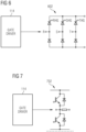
- Fig. 6 illustrates an example of the gate driver 114 connected to a plurality of power devices 602 that are mounted to (integrated within) the conductive substrate 104.
- the plurality of power devices 602 may comprise a rectifier comprised of 6 thyristors that may provide full inversion for 3 phases.
- Fig. 7 illustrates an example of the gate driver 114 connected to a plurality of power devices and a monitoring component that are mounted to (integrated within) the conductive substrate 104.
- Gate driver 114 may be coupled to two power devices forming a half-bridge.
- a shunt, for regulation and control of the output of the half-bridge e.g., the phase current or phase voltage
- the shunt may be formed on the conductive substrate 104.
- the shunt may be formed on the printed circuit board 112.
- An embodiment of the presently disclosed techniques comprises an apparatus.
- the apparatus comprises a power module housing including: a conductive substrate; a circuit board positioned overlying the conductive substrate; an insulation material electrically insulating the conductive substrate from the circuit board; a gate driver mounted to the circuit board; at least one power device mounted to the conductive substrate and controlled by the gate driver; and a monitoring component mounted to at least the conductive substrate and operatively coupled to the gate driver and the power device.
- the monitoring component is configured to turn off the at least one power device based on a parameter of the at least one power device.
- the monitoring component is configured to provide a signal indicative of a parameter of the at least one power device to the gate driver and wherein the gate driver is configured to turn off the at least one power device.
- the monitoring component is configured to provide a signal indicative of a parameter of the at least one power device to the gate driver and wherein the gate driver is configured to provide the signal to an external controller.
- the conductive substrate comprises one of a direct copper bonded (DCB) board and an insulated metal substrate (IMS) board.
- DCB direct copper bonded
- IMS insulated metal substrate
- the insulation material comprises a potting gel.
- the apparatus comprises a conductive connector electrically coupling the gate driver to at least one power device, wherein the insulation material is formed around the conductive connector and electrically insulates the gate driver from the power device.
- the apparatus comprises a conductive connector electrically coupling the conductive substrate to the circuit board, wherein the insulation material is formed around the conductive connector.
- the apparatus comprises a conductive connector electrically coupling the monitoring component to the circuit board, wherein the insulation material is formed around the conductive connector and electrically insulates the circuit board from the monitoring component.
- the apparatus comprises a circuit board connector coupled to the circuit board and providing connectivity outside the power module housing.
- the circuit board operates at a first voltage level and the conductive substrate operates at a second voltage level higher than the first voltage level.
- the monitoring component comprises an overcurrent protection device.
- the overcurrent protection device is formed by components on the conductive substrate, a conductive connector between the conductive substrate and the circuit board and components on the circuit board.
- the monitoring component comprises a temperature protection device.
- the apparatus comprises a plurality of power devices mounted on the conductive substrate, the plurality of power devices implementing one of a half bridge, a full bridge, a three-phase inverter, a rectifier, or a converter from AC to DC or AC or from DC to DC or AC.
- the monitoring component comprises a current measurement device or a voltage measurement device.
- the apparatus comprises an internal power supply mounted on the conductive substrate and providing power to at least the gate driver.
- An embodiment of the presently disclosed techniques comprises an apparatus.
- the apparatus comprises a power module housing including: a conductive substrate; a circuit board positioned adjacent the conductive substrate; an insulation material electrically insulating the conductive substrate from the circuit board; a gate driver mounted to the circuit board; a power device mounted to the conductive substrate and controlled by the gate driver; and a monitoring component mounted to at least the conductive substrate and operatively coupled to the gate driver and the power device.
- An embodiment of the presently disclosed techniques comprises an apparatus.
- the apparatus comprises a power module housing including: a conductive substrate; a circuit board positioned within the power module housing separate from the conductive substrate; an insulation material electrically insulating the conductive substrate from the circuit board; a gate driver mounted to the circuit board; a power device mounted to the conductive substrate and controlled by the gate driver; and a monitoring component mounted at least to the conductive substrate and operatively coupled the gate driver and the power device.
- the monitoring component comprise at least one of a current measurement device, a voltage measurement device, a temperature protection device, an overcurrent protection device, or a rectifier.
- any aspect or design described herein as an "example” is not necessarily to be construed as advantageous over other aspects or designs. Rather, use of the word “example” is intended to present one possible aspect and/or implementation that may pertain to the techniques presented herein. Such examples are not necessary for such techniques or intended to be limiting. Various embodiments of such techniques may include such an example, alone or in combination with other features, and/or may vary and/or omit the illustrated example.
- first,” “second,” or the like are not intended to imply a temporal aspect, a spatial aspect, an ordering, etc. Rather, such terms are merely used as identifiers, names, etc. for features, elements, items, etc.
- a first element and a second element generally correspond to element A and element B or two different or two identical elements or the same element.
Landscapes
- Engineering & Computer Science (AREA)
- Power Engineering (AREA)
- Microelectronics & Electronic Packaging (AREA)
- Power Conversion In General (AREA)
- Combinations Of Printed Boards (AREA)
- Emergency Protection Circuit Devices (AREA)
- Inverter Devices (AREA)
- Electronic Switches (AREA)
Applications Claiming Priority (1)
| Application Number | Priority Date | Filing Date | Title |
|---|---|---|---|
| US17/537,959 US12256514B2 (en) | 2021-11-30 | 2021-11-30 | Power module with integrated gate driver and functional components within a single power module housing |
Publications (2)
| Publication Number | Publication Date |
|---|---|
| EP4187585A2 true EP4187585A2 (fr) | 2023-05-31 |
| EP4187585A3 EP4187585A3 (fr) | 2023-08-30 |
Family
ID=84330276
Family Applications (1)
| Application Number | Title | Priority Date | Filing Date |
|---|---|---|---|
| EP22205806.7A Pending EP4187585A3 (fr) | 2021-11-30 | 2022-11-07 | Module de puissance avec circuit d'attaque de grille intégré et composants fonctionnels dans un seul boîtier de module de puissance |
Country Status (5)
| Country | Link |
|---|---|
| US (1) | US12256514B2 (fr) |
| EP (1) | EP4187585A3 (fr) |
| JP (1) | JP2023081347A (fr) |
| KR (1) | KR20230081673A (fr) |
| CN (1) | CN116207950A (fr) |
Cited By (1)
| Publication number | Priority date | Publication date | Assignee | Title |
|---|---|---|---|---|
| WO2026068573A1 (fr) * | 2024-09-25 | 2026-04-02 | Valeo Eautomotive Germany Gmbh | Module de puissance pour onduleur et circuit de collecte |
Families Citing this family (2)
| Publication number | Priority date | Publication date | Assignee | Title |
|---|---|---|---|---|
| USD1034492S1 (en) * | 2021-10-04 | 2024-07-09 | Transportation Ip Holdings, Llc | Housing for a full phase module gate drive |
| DE102023119155A1 (de) * | 2023-07-20 | 2025-01-23 | Dr. Ing. H.C. F. Porsche Aktiengesellschaft | Halbbrückenmodul, Halbbrückenmodulanordnung und Umrichter |
Family Cites Families (8)
| Publication number | Priority date | Publication date | Assignee | Title |
|---|---|---|---|---|
| US6490162B2 (en) * | 2000-08-24 | 2002-12-03 | International Rectifier Corporation | Heatsink retainer |
| US7911792B2 (en) * | 2008-03-11 | 2011-03-22 | Ford Global Technologies Llc | Direct dipping cooled power module and packaging |
| EP2538761B1 (fr) * | 2011-06-20 | 2014-01-29 | STMicroelectronics Srl | Module d'alimentation intelligente et procédé d'assemblage associé |
| TWI516028B (zh) | 2013-06-20 | 2016-01-01 | 財團法人工業技術研究院 | 高低壓隔離內埋功率模組 |
| ITUB20153344A1 (it) | 2015-09-02 | 2017-03-02 | St Microelectronics Srl | Modulo di potenza elettronico con migliorata dissipazione termica e relativo metodo di fabbricazione |
| US9972569B2 (en) * | 2016-04-12 | 2018-05-15 | General Electric Company | Robust low inductance power module package |
| EP3404774B1 (fr) | 2017-05-17 | 2021-10-06 | Infineon Technologies AG | Procédé de connexion électrique d'un module électronique et ensemble électronique |
| TWI752398B (zh) * | 2020-01-02 | 2022-01-11 | 財團法人工業技術研究院 | 功率模組 |
-
2021
- 2021-11-30 US US17/537,959 patent/US12256514B2/en active Active
-
2022
- 2022-11-07 EP EP22205806.7A patent/EP4187585A3/fr active Pending
- 2022-11-21 CN CN202211473111.5A patent/CN116207950A/zh active Pending
- 2022-11-29 KR KR1020220162826A patent/KR20230081673A/ko active Pending
- 2022-11-29 JP JP2022189835A patent/JP2023081347A/ja active Pending
Cited By (1)
| Publication number | Priority date | Publication date | Assignee | Title |
|---|---|---|---|---|
| WO2026068573A1 (fr) * | 2024-09-25 | 2026-04-02 | Valeo Eautomotive Germany Gmbh | Module de puissance pour onduleur et circuit de collecte |
Also Published As
| Publication number | Publication date |
|---|---|
| CN116207950A (zh) | 2023-06-02 |
| US20230170791A1 (en) | 2023-06-01 |
| JP2023081347A (ja) | 2023-06-09 |
| EP4187585A3 (fr) | 2023-08-30 |
| US12256514B2 (en) | 2025-03-18 |
| KR20230081673A (ko) | 2023-06-07 |
Similar Documents
| Publication | Publication Date | Title |
|---|---|---|
| US12256514B2 (en) | Power module with integrated gate driver and functional components within a single power module housing | |
| JP7230048B2 (ja) | 電子電源スイッチ駆動モジュール | |
| US7834575B2 (en) | Gate-driver IC with HV-isolation, especially hybrid electric vehicle motor drive concept | |
| CN101682291B (zh) | 电机控制装置 | |
| US10134718B2 (en) | Power semiconductor module | |
| US20120063187A1 (en) | Inverter device | |
| US11071225B2 (en) | Smart high-voltage relay | |
| CN104851879A (zh) | 具低电感配置内部负载和辅助连接装置的功率半导体模块 | |
| CN110999055B (zh) | 用于快速电流感测和晶体管时序控制的系统和方法 | |
| US20240014107A1 (en) | Semiconductor device | |
| EP3432460B1 (fr) | Convertisseur d'énergie | |
| JP2013222885A (ja) | インバータモジュール | |
| US20240188263A1 (en) | Power module for a converter with improved field shielding of signal pins | |
| US8669648B2 (en) | Power semiconductor module | |
| US11050358B2 (en) | Power module with built-in drive circuit | |
| KR102117719B1 (ko) | 전력 반도체 회로 | |
| CN107710580B (zh) | 用于转换器的快速开关的电路装置 | |
| CN100490293C (zh) | 电力变换装置 | |
| US9866102B2 (en) | Power conversion device | |
| EP3731605A1 (fr) | Agencement de circuit électrique pour convertisseur de puissance | |
| US7760480B2 (en) | Electronic assembly for switching electric power | |
| US20240312877A1 (en) | Semiconductor device | |
| JP2009273272A (ja) | インバータモジュール | |
| US20230307332A1 (en) | Power Semiconductor Module and Method for Producing a Power Semiconductor Module | |
| JP5991136B2 (ja) | 電力変換装置 |
Legal Events
| Date | Code | Title | Description |
|---|---|---|---|
| PUAI | Public reference made under article 153(3) epc to a published international application that has entered the european phase |
Free format text: ORIGINAL CODE: 0009012 |
|
| STAA | Information on the status of an ep patent application or granted ep patent |
Free format text: STATUS: THE APPLICATION HAS BEEN PUBLISHED |
|
| AK | Designated contracting states |
Kind code of ref document: A2 Designated state(s): AL AT BE BG CH CY CZ DE DK EE ES FI FR GB GR HR HU IE IS IT LI LT LU LV MC ME MK MT NL NO PL PT RO RS SE SI SK SM TR |
|
| PUAL | Search report despatched |
Free format text: ORIGINAL CODE: 0009013 |
|
| AK | Designated contracting states |
Kind code of ref document: A3 Designated state(s): AL AT BE BG CH CY CZ DE DK EE ES FI FR GB GR HR HU IE IS IT LI LT LU LV MC ME MK MT NL NO PL PT RO RS SE SI SK SM TR |
|
| RIC1 | Information provided on ipc code assigned before grant |
Ipc: H02M 7/00 20060101ALI20230725BHEP Ipc: H01L 23/538 20060101ALI20230725BHEP Ipc: H01L 25/16 20230101ALI20230725BHEP Ipc: H01L 25/07 20060101ALI20230725BHEP Ipc: H01L 23/04 20060101AFI20230725BHEP |
|
| STAA | Information on the status of an ep patent application or granted ep patent |
Free format text: STATUS: REQUEST FOR EXAMINATION WAS MADE |
|
| 17P | Request for examination filed |
Effective date: 20240131 |
|
| RBV | Designated contracting states (corrected) |
Designated state(s): AL AT BE BG CH CY CZ DE DK EE ES FI FR GB GR HR HU IE IS IT LI LT LU LV MC ME MK MT NL NO PL PT RO RS SE SI SK SM TR |