EP4187723A1 - Élément de contact électriquement conducteur pour un connecteur - Google Patents
Élément de contact électriquement conducteur pour un connecteur Download PDFInfo
- Publication number
- EP4187723A1 EP4187723A1 EP21306644.2A EP21306644A EP4187723A1 EP 4187723 A1 EP4187723 A1 EP 4187723A1 EP 21306644 A EP21306644 A EP 21306644A EP 4187723 A1 EP4187723 A1 EP 4187723A1
- Authority
- EP
- European Patent Office
- Prior art keywords
- electrically conductive
- contact element
- face
- conductive contact
- depression
- Prior art date
- Legal status (The legal status is an assumption and is not a legal conclusion. Google has not performed a legal analysis and makes no representation as to the accuracy of the status listed.)
- Pending
Links
Images


Classifications
-
- H—ELECTRICITY
- H01—ELECTRIC ELEMENTS
- H01R—ELECTRICALLY-CONDUCTIVE CONNECTIONS; STRUCTURAL ASSOCIATIONS OF A PLURALITY OF MUTUALLY-INSULATED ELECTRICAL CONNECTING ELEMENTS; COUPLING DEVICES; CURRENT COLLECTORS
- H01R13/00—Details of coupling devices of the kinds covered by groups H01R12/70 or H01R24/00 - H01R33/00
- H01R13/02—Contact members
- H01R13/03—Contact members characterised by the material, e.g. plating, or coating materials
-
- B—PERFORMING OPERATIONS; TRANSPORTING
- B32—LAYERED PRODUCTS
- B32B—LAYERED PRODUCTS, i.e. PRODUCTS BUILT-UP OF STRATA OF FLAT OR NON-FLAT, e.g. CELLULAR OR HONEYCOMB, FORM
- B32B15/00—Layered products comprising a layer of metal
- B32B15/20—Layered products comprising a layer of metal comprising aluminium or copper
-
- B—PERFORMING OPERATIONS; TRANSPORTING
- B32—LAYERED PRODUCTS
- B32B—LAYERED PRODUCTS, i.e. PRODUCTS BUILT-UP OF STRATA OF FLAT OR NON-FLAT, e.g. CELLULAR OR HONEYCOMB, FORM
- B32B3/00—Layered products comprising a layer with external or internal discontinuities or unevennesses, or a layer of non-planar shape; Layered products comprising a layer having particular features of form
- B32B3/26—Layered products comprising a layer with external or internal discontinuities or unevennesses, or a layer of non-planar shape; Layered products comprising a layer having particular features of form characterised by a particular shape of the outline of the cross-section of a continuous layer; characterised by a layer with cavities or internal voids ; characterised by an apertured layer
- B32B3/263—Layered products comprising a layer with external or internal discontinuities or unevennesses, or a layer of non-planar shape; Layered products comprising a layer having particular features of form characterised by a particular shape of the outline of the cross-section of a continuous layer; characterised by a layer with cavities or internal voids ; characterised by an apertured layer characterised by a layer having non-uniform thickness
-
- B—PERFORMING OPERATIONS; TRANSPORTING
- B32—LAYERED PRODUCTS
- B32B—LAYERED PRODUCTS, i.e. PRODUCTS BUILT-UP OF STRATA OF FLAT OR NON-FLAT, e.g. CELLULAR OR HONEYCOMB, FORM
- B32B3/00—Layered products comprising a layer with external or internal discontinuities or unevennesses, or a layer of non-planar shape; Layered products comprising a layer having particular features of form
- B32B3/26—Layered products comprising a layer with external or internal discontinuities or unevennesses, or a layer of non-planar shape; Layered products comprising a layer having particular features of form characterised by a particular shape of the outline of the cross-section of a continuous layer; characterised by a layer with cavities or internal voids ; characterised by an apertured layer
- B32B3/30—Layered products comprising a layer with external or internal discontinuities or unevennesses, or a layer of non-planar shape; Layered products comprising a layer having particular features of form characterised by a particular shape of the outline of the cross-section of a continuous layer; characterised by a layer with cavities or internal voids ; characterised by an apertured layer characterised by a layer formed with recesses or projections, e.g. hollows, grooves, protuberances, ribs
-
- B—PERFORMING OPERATIONS; TRANSPORTING
- B32—LAYERED PRODUCTS
- B32B—LAYERED PRODUCTS, i.e. PRODUCTS BUILT-UP OF STRATA OF FLAT OR NON-FLAT, e.g. CELLULAR OR HONEYCOMB, FORM
- B32B7/00—Layered products characterised by the relation between layers; Layered products characterised by the relative orientation of features between layers, or by the relative values of a measurable parameter between layers, i.e. products comprising layers having different physical, chemical or physicochemical properties; Layered products characterised by the interconnection of layers
- B32B7/04—Interconnection of layers
- B32B7/12—Interconnection of layers using interposed adhesives or interposed materials with bonding properties
-
- H—ELECTRICITY
- H01—ELECTRIC ELEMENTS
- H01R—ELECTRICALLY-CONDUCTIVE CONNECTIONS; STRUCTURAL ASSOCIATIONS OF A PLURALITY OF MUTUALLY-INSULATED ELECTRICAL CONNECTING ELEMENTS; COUPLING DEVICES; CURRENT COLLECTORS
- H01R13/00—Details of coupling devices of the kinds covered by groups H01R12/70 or H01R24/00 - H01R33/00
- H01R13/02—Contact members
- H01R13/15—Pins, blades or sockets having separate spring member for producing or increasing contact pressure
-
- H—ELECTRICITY
- H01—ELECTRIC ELEMENTS
- H01R—ELECTRICALLY-CONDUCTIVE CONNECTIONS; STRUCTURAL ASSOCIATIONS OF A PLURALITY OF MUTUALLY-INSULATED ELECTRICAL CONNECTING ELEMENTS; COUPLING DEVICES; CURRENT COLLECTORS
- H01R43/00—Apparatus or processes specially adapted for manufacturing, assembling, maintaining, or repairing of line connectors or current collectors or for joining electric conductors
- H01R43/16—Apparatus or processes specially adapted for manufacturing, assembling, maintaining, or repairing of line connectors or current collectors or for joining electric conductors for manufacturing contact members, e.g. by punching and by bending
-
- B—PERFORMING OPERATIONS; TRANSPORTING
- B32—LAYERED PRODUCTS
- B32B—LAYERED PRODUCTS, i.e. PRODUCTS BUILT-UP OF STRATA OF FLAT OR NON-FLAT, e.g. CELLULAR OR HONEYCOMB, FORM
- B32B2307/00—Properties of the layers or laminate
- B32B2307/20—Properties of the layers or laminate having particular electrical or magnetic properties, e.g. piezoelectric
- B32B2307/202—Conductive
-
- B—PERFORMING OPERATIONS; TRANSPORTING
- B32—LAYERED PRODUCTS
- B32B—LAYERED PRODUCTS, i.e. PRODUCTS BUILT-UP OF STRATA OF FLAT OR NON-FLAT, e.g. CELLULAR OR HONEYCOMB, FORM
- B32B2307/00—Properties of the layers or laminate
- B32B2307/70—Other properties
- B32B2307/732—Dimensional properties
- B32B2307/737—Dimensions, e.g. volume or area
-
- B—PERFORMING OPERATIONS; TRANSPORTING
- B32—LAYERED PRODUCTS
- B32B—LAYERED PRODUCTS, i.e. PRODUCTS BUILT-UP OF STRATA OF FLAT OR NON-FLAT, e.g. CELLULAR OR HONEYCOMB, FORM
- B32B2457/00—Electrical equipment
Definitions
- the present invention relates to an electrically conductive contact element for a connector which has a contact surface, and an electrical connector comprising such an electrically conductive contact element.
- the present invention further relates to a method of manufacturing the contact surface of an electrically conductive contact element for an electrical connector.
- Electrical connectors are generally used for signal or power transmission and to link electrical and electronic systems. Electrical connectors are provided with electrically conductive contact elements, which come into contact with a contact element of a mating electrical connector when the electrical connector is plugged to the mating electrical connector.
- the contact elements of the connector element are commonly formed as contact pins and those of the mating connector are commonly formed as contact springs. When the connector and mating connector are coupled, the contact springs exert elastic spring forces on the contact pins and thereby provide an electrical connection between the contact elements.
- the quality of the electrical connection may be affected by mechanical and/or chemical degradations occurring at the contact surfaces of the contact elements.
- the respective contact surface of the electrically conductive contact elements may be coated with a layer of tin, nickel or alloys thereof.
- the spatial dimensions in the caverns according to US 2019/0173214 A1 is in the range of 0,1-50 micrometers.
- the arrangement of the caverns according to US 2019/0173214 A1 under the contact surface is such that an outlet of the cavern is tight enough so that the lubricant filled into the caverns cannot be accessed without establishing an opening from the contact surfaces into the cavern.
- Manufacturing the microstructure US 2019/0173214 A1 requires the use of a laser, an electron beam or surface treatment like masking and etching.
- the object of the present invention is to provide an improved and cost effective contact element for a connector which can better withstand wear so as to reduce the contact resistance while reducing the mating force to ease the assembly and the maintenance of the connector, in particular without the need of using lubricant.
- the object of the present invention is achieved by means of an electrically conductive contact element for an electrical connector according to claim 1.
- the electrically conductive contact element has a contact surface configured to be brought into contact with a surface of a connecting part of a mating electrical connector adapted to be mated with the electrical connector.
- the electrically conductive contact element comprises: a body and a layer of an electrically conductive material provided on a first face of said body, wherein the contact surface is formed by a surface of said layer facing away from the body.
- the first face of the body comprises at least one depression forming a reservoir filled with the electrically conductive material.
- the electrically conductive contact element is provided with the electrically conductive material contained in the layer as well as with the electrically conductive material filled in the reservoir.
- the at least one depression under the contact surface, there is more electrically conductive material than in the rest of the electrically conductive contact element, wherein the first face of the body is covered by the layer of the electrically conductive material.
- an uneven wear of the contact surface is caused, such that presence of the electrically conductive material can last longer at the at least one depression. Consequently, the at least one depression provides a contact area that is preserved longer from mechanical wear and corrosion during the lifetime of the electrically conductive contact element.
- the resistance to the outdoor environment, like corrosive media and the electrical constriction resistance at the at least one depression is improved over the lifetime of the electrically conductive contact element with respect to the known contact element. It allows increasing the durability of an electrical connector comprising such electrically conductive contact element by preventing, or at least delaying, a malfunction of the connector related to the quality of the electrical contact. Moreover, as the presence of electrically conductive material allows reducing the required mating force thank to the mechanical properties of the electrically conductive material, the ease of assembly, plugging and handling of a related electrical connector can be enhanced.
- the electrically conductive contact element can be further improved according to various advantageous embodiments.
- the embodiments are disclosed in the dependent claims.
- the electrically conductive material filled in the reservoir can be configured to come in contact with a surface of a connecting part of the mating electrical connector.
- the reservoir has a direct output at the contact surface. It allows directly exposing the electrically conductive material to a mating contact surface.
- the body can be made of metal and the electrically conductive material can be a plating material made of tin, nickel, silver, gold, a tin-nickel alloy, an alloy of tin or a nickel-silver alloy.
- Electrically conductive materials are selected so as to enable an electrical connection between electrical connectors.
- the plating material can be selected based on its resistance to mechanical wear and/or corrosion, as well as its cost and availability.
- a minimum dimension of the at least one depression in a plan of the contact surface can be greater than 0,05mm, in particular can be comprised between 0,05mm and 0,06mm.
- the at least one depression does not form a microstructure in the first face of the body.
- manufacturing means require for forming a microstructure, like laser, electron beam or masking and etching.
- a maximal depth of the at least one depression can be greater than 0,03mm, in particular greater than 0,04mm, more in particular more than 0,05mm.
- the at least one depression does not form a microstructure in the first face of the body.
- manufacturing means require for forming a microstructure, like laser, electron beam or masking and etching.
- the maximal depth can be adapted so as to improve further and longer the resistance to wear, by increasing the size of the reservoir of electrically conductive material.
- the at least one depression can have a half-spherical shape or a groove shape, in particular a rounded groove shape.
- Half-spherical and round shapes allow avoiding the presence of sharp edges and optimizing the amount of electrically conductive material filled in the reservoir.
- a groove shape allows providing reservoir that may advantageously extend along a direction of a back and forth motion of the mating contact surfaces, for example a motion caused by vibrations.
- the electrically conductive contact element can further comprise an adhesion layer provided on the first face of the body and sandwiched between the first face and the layer of the electrically conductive material.
- the quality of the electrical contact over time can be further improved by the use of an adhesion layer.
- a thickness of the electrically conductive material in the at least one depression, can be greater than a thickness of the adhesion layer.
- the reservoir is filled with a sufficient amount of electrically conductive material to provide the technical effects of improving the resistance to wear and corrosion and reducing the electrical constriction resistance and the required mating force.
- the adhesion layer can be made of nickel, copper or tin.
- the electrically conductive contact element can comprise a plurality of depressions and a minimum spacing distance between the depressions can be comprised between 0,10mm and 0,15mm.
- the plurality of depressions provide a redundancy of improved contact areas, thereby enhancing the reliability and durability of the electrical contact between electrical connectors.
- the first face of the body can comprise at least one curved region curved in at least one direction and the at least one depression can be arranged at the at least one curved region.
- Curved region can provide a region that is more subjected to deformation than the other regions under elastic spring forces. By increasing the mechanical contact performance at the curved region, the electrical contact performance can be improved as well. Hence, it is particularly advantageous to arrange the at least one depression at the curved region.
- the first face of the body can comprise a plurality of depressions of different shapes and/or sizes.
- the design of the depressions can be advantageously adapted to the contact zone with a mating connector based on the force applied, the size of the contact zone etc.
- the electrically conductive contact element can be comprised in an electrical connector configured to be coupled with a mating electrical connector.
- an electrical connector configured to be coupled with a mating electrical connector, comprising an electrically conductive contact element.
- Said electrically conductive contact element comprising: a body having at least a first face, and a layer of an electrically conductive material provided on said first face of the body, the first face of the body comprising at least one depression forming a reservoir filled with the electrically conductive material, and a contact surface configured to be brought into contact with a surface of a connecting part of a mating electrical connector and formed by a surface of said layer of the electrically conductive material facing away from the body.
- the electrically conductive contact element is provided under the contact surface with the electrically conductive material contained in the layer as well as with the electrically conductive material filled in the reservoir.
- the contact surface made of the electrically conductive material is thicker than in the rest of the electrically conductive contact element.
- the resistance to the outdoor environment, like corrosive media and the electrical constriction resistance at the at least one depression is improved over the lifetime of the electrically conductive contact element of the electrical connector with respect to the known electrical connectors. It allows increasing the durability of the electrical connector by preventing, or at least delaying, a malfunction of the connector related to the quality of the electrical contact. Moreover, as the presence of electrically conductive material allows reducing the required mating force thank to the mechanical properties of the electrically conductive material, the ease of assembly, plugging and handling of the electrical connector can be enhanced.
- the object of the invention is also achieved by a method of manufacturing a contact surface of an electrically conductive contact element, comprising the steps of: a) forming at least one depression in a first face of a body of the electrically conductive contact element, in particular by metal punching, and then b) applying a layer of an electrically conductive material on the first face including filling the at least one depression with the electrically conductive material.
- the method of manufacturing allows providing a contact surface wherein at the at least one depression, under the contact surface, there is more electrically conductive material than in the rest of the electrically conductive contact element, wherein the first face of the body is covered by the layer of the electrically conductive material.
- an uneven wear of the contact surface is caused, such that presence of the electrically conductive material can last longer at the at least one depression. Consequently, the at least one depression provides a contact area that is preserved longer from mechanical wear and corrosion during the lifetime of the electrically conductive contact element. Accordingly, the resistance to the outdoor environment, like corrosive media and the electrical constriction resistance at the at least one depression is improved over the lifetime of the electrically conductive contact element with respect to the known contact element.
- the method of manufacturing can further comprise, before the step b), a step of applying an adhesion layer on the contact surface.
- the step of adding an adhesion layer allows further improving the quality of the electrical contact throughout the lifetime of the electrical connector.
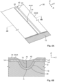
- Figure 1 and Figure 2 illustrate a partial cross-sectional view of a body of an electrically conductive contact element 10 according to a first embodiment of the present invention.
- a contact surface is represented, while in Figure 2 the contact surface is omitted in order to better highlight the structure of the body of the electrically conductive contact element 10.
- Figure 1 and Figure 2 are described together in the following.
- the electrically conductive contact element 10 for an electrical connector comprises a body 12, in particular a metallic body 12.
- the body 12 is delimited by a plurality of faces.
- at least one face 14 of the body 12, said face 14 extending in a plan (XY) in the example of Figures 1 and 2 is provided with a depression 16.
- the depression 16 extends from an opening 18 in the face 14 partially into the body 12 along a direction parallel to the axis Z.
- the depression 16 has a substantially half-spherical shape.
- the diameter L1 of the corresponding circular opening 18 can be greater than 0,05mm, in particular can be comprised between 0,05mm and 0,06mm.
- the maximal depth L2 of the depression 16 is greater than 0,01mm. Namely, the maximal depth L2 of the depression 16 can be greater than 0,03mm, in particular greater than 0,04mm, more in particular greater than 0,05mm.
- the depression 16 can have a groove shape, in particular a rounded groove shape.
- the opening 18 of the depression 16 can have a square shape, a rectangular shape, an oval shape, triangular shape, etc.
- the depression 16 forms a reservoir 20.
- Figure 2 illustrates an empty reservoir 20 in order to better highlight the structure of the depression 16.
- the depression 16 has one open-end 18.
- a layer 22 of an electrically conductive material M of thickness L3 is provided on the face 14 of the body 12.
- the electrically conductive material M is a plating material that can be made of tin, nickel, silver, gold, a tin-nickel alloy, an alloy of tin or nickel-silver alloy.
- the layer 22 of the electrically conductive material M is directly provided on the face 14.
- a surface 24 of the layer 22 facing away from the body 12 of the electrically conductive contact element 10 forms a contact surface 24.
- the contact surface 24 extends substantially in the plane (XY).
- the contact surface 24 is configured to be brought into contact with a surface of a connecting part of a mating electrical connector (not represented).
- the initial stage relates to a stage wherein the electrically conductive contact element 10 has not yet being brought in contact with an electrically conductive contact element of a mating connector.
- the contact surface 24 is substantially flat in the plane (XY).
- Figure 3 illustrates a partial cross-sectional view of a body of an electrically conductive contact element 30 according to a second embodiment of the present invention.
- an adhesion layer 32 is directly provided on the face 14 of the body 12 and sandwiched between the face 14 of the body 12 and the layer 22 of the electrically conductive material M.
- the adhesion layer 32 is provided with a substantially uniform thickness L4 on the face 14, including on the face 14 in the depression 16, as shown in Figure 3 .
- the layer 22 has a thickness L3', wherein L3' ⁇ L3.
- further layers may be sandwiched between the face 14 of the body 12 and the layer 22 of the electrically conductive material M.
- Figure 4A illustrates a top view of the electrically conductive contact element 30 according to the second embodiment of the present invention at a later stage than the initial stage, wherein mechanical and/or chemical wear has occurred.
- Figure 4B illustrates a cross-sectional view of the electrically conductive contact element 30 shown in Figure 4A.
- Figure 4A and Figure 4B are described together in the following.
- the mechanical and/chemical wear has caused a disruption 40 in the contact surface 24 leading to the exposure of the adhesion layer 32.
- the disruption 40 has the shape of a groove 42 extending along the axis X.
- Such linear groove shape may be caused by a back and forth motion of the mating contact surfaces for example.
- Other shapes (not represented) of disruption 40 in the contact surface 24 may occur, depending on the relative motions of the connector and the mating connector for instance.
- the presence of the depression 16 in the body 12 allows providing a reservoir 20 of electrically conductive material M such that at the wear stage of Figures 4A and 4B , a contact area 44 of electrically conductive material M still remains at the contact surface 24 despite the disruption 40.
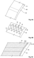
- Figure 5 illustrates an enlarged view of an electrically conductive contact element 50 according to a third embodiment of the present invention.
- the electrically conductive material M and the optional adhesive layer 52 is not represented in Figure 5 .
- the electrically conductive contact element 50 has a metallic body 52 comprising a frame 54 extending in a plane (XY) and defining an aperture 56.
- a metallic body 52 comprising a frame 54 extending in a plane (XY) and defining an aperture 56.
- Four contact pins 58 extends within the frame 54 across the aperture 56.
- the number of contact pins 58 is not limitative.
- Each contact pins 58 are bent with respect to the plan (XY) such as to be provided with two slightly curved regions R1 and R2. The number of curved regions is not limitative.
- the curved regions R1, R2 consist of the regions of the electrically conductive contact element 50 onto which greater elastic spring forces are exerted in comparison with the rest of the contact pins 58. Elastic spring forces is intended to be exerted on the curved regions R1, R2 by a connecting part of a mating connector applying a pressure on the curved regions R1, R2 in a mating state of the connectors.
- the curved regions R1, R2 are provided with a plurality of depressions 16 formed in the face 14 of the metallic body 52, as previously described in reference to Figures 1 and 2 .
- the location of the plurality of depressions 16 at the curved regions R1, R2 allows improving the wear resistance at the area most subject to mechanical stress, and therefore to wear.
- the plurality of depressions 16 provide a redundancy of improved contact areas, thereby enhancing the reliability and durability of the electrical contact between the electrical connectors.
- Figures 6A , 6B and 6C illustrate successive steps of a method of manufacturing a contact surface of the electrically conductive contact element 50 according to the third embodiment of the present invention.
- the face 14 of the metallic body 12 at the contact pin 58 is substantially uniform.
- each depression 16 has a substantially half-spherical shape.
- the depressions 16 can have a different shape than a substantially half-spherical shape.
- the plurality of depressions 16 can comprise a combination of depressions 16 of different shapes and/or sizes.
- a plating layer 22 of the electrically conductive material M of thickness L5 has been provided on the face 14 of the metallic body 12 thereby coating the face 14 and filling each depression 16 with the electrically conductive material M.
- the surface 24 of the plating layer 22 facing away from the body 52 forms the contact surface 24 of the electrically conductive contact element 50.
Landscapes
- Engineering & Computer Science (AREA)
- Manufacturing & Machinery (AREA)
- Manufacturing Of Electrical Connectors (AREA)
Priority Applications (6)
| Application Number | Priority Date | Filing Date | Title |
|---|---|---|---|
| EP21306644.2A EP4187723A1 (fr) | 2021-11-25 | 2021-11-25 | Élément de contact électriquement conducteur pour un connecteur |
| JP2022185380A JP7858510B2 (ja) | 2021-11-25 | 2022-11-21 | コネクタ用導電性コンタクト要素 |
| CN202211466205.XA CN116169500A (zh) | 2021-11-25 | 2022-11-22 | 用于连接器的导电接触元件 |
| US17/993,151 US12489236B2 (en) | 2021-11-25 | 2022-11-23 | Electrically conductive contact element for a connector |
| KR1020220158285A KR20230077681A (ko) | 2021-11-25 | 2022-11-23 | 커넥터를 위한 전기 전도성 접점 요소 |
| JP2024157922A JP2024167432A (ja) | 2021-11-25 | 2024-09-12 | コネクタ用導電性コンタクト要素 |
Applications Claiming Priority (1)
| Application Number | Priority Date | Filing Date | Title |
|---|---|---|---|
| EP21306644.2A EP4187723A1 (fr) | 2021-11-25 | 2021-11-25 | Élément de contact électriquement conducteur pour un connecteur |
Publications (1)
| Publication Number | Publication Date |
|---|---|
| EP4187723A1 true EP4187723A1 (fr) | 2023-05-31 |
Family
ID=78851028
Family Applications (1)
| Application Number | Title | Priority Date | Filing Date |
|---|---|---|---|
| EP21306644.2A Pending EP4187723A1 (fr) | 2021-11-25 | 2021-11-25 | Élément de contact électriquement conducteur pour un connecteur |
Country Status (5)
| Country | Link |
|---|---|
| US (1) | US12489236B2 (fr) |
| EP (1) | EP4187723A1 (fr) |
| JP (2) | JP7858510B2 (fr) |
| KR (1) | KR20230077681A (fr) |
| CN (1) | CN116169500A (fr) |
Families Citing this family (1)
| Publication number | Priority date | Publication date | Assignee | Title |
|---|---|---|---|---|
| KR20240176697A (ko) | 2023-06-16 | 2024-12-24 | 주식회사 엘지에너지솔루션 | 릴레이 제어 장치 및 방법 |
Citations (4)
| Publication number | Priority date | Publication date | Assignee | Title |
|---|---|---|---|---|
| US20080257581A1 (en) * | 2007-04-20 | 2008-10-23 | Kabushiki Kaisha Kobe Seiko Sho (Kobe Steel, Ltd) | Terminal for engaging type connector |
| US20130014979A1 (en) * | 2011-07-15 | 2013-01-17 | Tessera, Inc. | Connector Structures and Methods |
| US20190173214A1 (en) | 2016-08-08 | 2019-06-06 | Te Connectivity Germany Gmbh | Electrical Contact Element For An Electrical Connector Having Microstructured Caverns Under The Contact Surface |
| WO2020049988A1 (fr) * | 2018-09-06 | 2020-03-12 | 株式会社デンソー | Méthode de production de produit plaqué |
Family Cites Families (23)
| Publication number | Priority date | Publication date | Assignee | Title |
|---|---|---|---|---|
| EP1014494A1 (fr) * | 1998-12-16 | 2000-06-28 | Zurecon Ag | Méthode pour joindre conducteurs de courant métalliques et une connexion d'une barre omnibus fabriquée selon cette méthode |
| US7192495B1 (en) * | 2003-08-29 | 2007-03-20 | Micron Technology, Inc. | Intermediate anneal for metal deposition |
| EP1788585B1 (fr) * | 2004-09-10 | 2015-02-18 | Kabushiki Kaisha Kobe Seiko Sho (Kobe Steel, Ltd.) | Matériau conducteur pour pièce de connexion et procédé de fabrication du matériau conducteur |
| JP5128153B2 (ja) * | 2006-03-17 | 2013-01-23 | 古河電気工業株式会社 | 電気接点材料及びその製造方法 |
| EP1840917B1 (fr) * | 2006-03-27 | 2013-09-25 | Abb Ab | Contacteur électrique |
| JP5464792B2 (ja) * | 2007-04-20 | 2014-04-09 | 株式会社神戸製鋼所 | 嵌合型コネクタ用端子の製造方法 |
| JP5025387B2 (ja) * | 2007-08-24 | 2012-09-12 | 株式会社神戸製鋼所 | 接続部品用導電材料及びその製造方法 |
| US8956735B2 (en) * | 2010-03-26 | 2015-02-17 | Kabushiki Kaisha Kobe Seiko Sho | Copper alloy and electrically conductive material for connecting parts, and mating-type connecting part and method for producing the same |
| JP5260620B2 (ja) * | 2010-12-07 | 2013-08-14 | 株式会社神戸製鋼所 | Pcb端子及びその製造方法 |
| DE102011088793A1 (de) * | 2011-12-16 | 2013-06-20 | Tyco Electronics Amp Gmbh | Elektrischer Steckverbinder mit mikrostrukturiertem Kontaktelement |
| JP5829937B2 (ja) * | 2012-02-15 | 2015-12-09 | 矢崎総業株式会社 | 端子接続構造 |
| US20150236439A1 (en) * | 2012-08-31 | 2015-08-20 | Autonetworks Technologies, Ltd. | Plated terminal for connector, and terminal pair |
| US9543679B2 (en) * | 2012-10-05 | 2017-01-10 | Tyco Electronics Corporation | Electrical contact assembly |
| JP5975903B2 (ja) * | 2013-02-21 | 2016-08-23 | 株式会社神戸製鋼所 | 嵌合型コネクタ用端子 |
| DE102013203273B4 (de) * | 2013-02-27 | 2017-02-23 | S-Y Systems Technologies Europe Gmbh | Kontaktelement |
| JP2015109198A (ja) * | 2013-12-04 | 2015-06-11 | 株式会社オートネットワーク技術研究所 | コネクタ端子 |
| WO2015125682A1 (fr) * | 2014-02-18 | 2015-08-27 | 矢崎総業株式会社 | Borne de connexion |
| DE112015001904T5 (de) * | 2014-04-24 | 2016-12-29 | Yazaki Corporation | Kontaktverbindungsstruktur |
| JP6420567B2 (ja) * | 2014-05-19 | 2018-11-07 | 矢崎総業株式会社 | 端子および端子の製造方法 |
| DE102015209855A1 (de) * | 2015-05-28 | 2016-12-01 | Te Connectivity Germany Gmbh | Elektrisches Kontaktierungselement mit einer feinstrukturierten Kontaktierungsfläche |
| JP6677508B2 (ja) * | 2015-12-25 | 2020-04-08 | 矢崎総業株式会社 | メス端子 |
| WO2017150345A1 (fr) * | 2016-03-01 | 2017-09-08 | 矢崎総業株式会社 | Structure de contact de borne et procédé de fabrication de structure de contact de borne |
| JP7388221B2 (ja) * | 2020-02-10 | 2023-11-29 | 住友電装株式会社 | 雄端子金具および端子構造 |
-
2021
- 2021-11-25 EP EP21306644.2A patent/EP4187723A1/fr active Pending
-
2022
- 2022-11-21 JP JP2022185380A patent/JP7858510B2/ja active Active
- 2022-11-22 CN CN202211466205.XA patent/CN116169500A/zh active Pending
- 2022-11-23 US US17/993,151 patent/US12489236B2/en active Active
- 2022-11-23 KR KR1020220158285A patent/KR20230077681A/ko not_active Ceased
-
2024
- 2024-09-12 JP JP2024157922A patent/JP2024167432A/ja active Pending
Patent Citations (4)
| Publication number | Priority date | Publication date | Assignee | Title |
|---|---|---|---|---|
| US20080257581A1 (en) * | 2007-04-20 | 2008-10-23 | Kabushiki Kaisha Kobe Seiko Sho (Kobe Steel, Ltd) | Terminal for engaging type connector |
| US20130014979A1 (en) * | 2011-07-15 | 2013-01-17 | Tessera, Inc. | Connector Structures and Methods |
| US20190173214A1 (en) | 2016-08-08 | 2019-06-06 | Te Connectivity Germany Gmbh | Electrical Contact Element For An Electrical Connector Having Microstructured Caverns Under The Contact Surface |
| WO2020049988A1 (fr) * | 2018-09-06 | 2020-03-12 | 株式会社デンソー | Méthode de production de produit plaqué |
Also Published As
| Publication number | Publication date |
|---|---|
| JP7858510B2 (ja) | 2026-05-14 |
| JP2024167432A (ja) | 2024-12-03 |
| CN116169500A (zh) | 2023-05-26 |
| US20230163504A1 (en) | 2023-05-25 |
| US12489236B2 (en) | 2025-12-02 |
| KR20230077681A (ko) | 2023-06-01 |
| JP2023078092A (ja) | 2023-06-06 |
Similar Documents
| Publication | Publication Date | Title |
|---|---|---|
| JP7453280B2 (ja) | コネクタシステム | |
| KR101389172B1 (ko) | 암형 단자 피팅 및 그 제조 방법 | |
| CN105706308B (zh) | 电连接装置 | |
| KR20010015447A (ko) | 테스트용 소켓, 그 제조 방법, 테스트용 소켓을 이용한테스트 방법, 및 피 테스트 부재 | |
| EP2752945A2 (fr) | Borne de connexion de type appariée et procédé de fabrication pour celle-ci | |
| EP3089277B1 (fr) | Module électronique véhiculaire | |
| US11239593B2 (en) | Electrical contact element for an electrical connector having microstructured caverns under the contact surface | |
| KR20150123182A (ko) | 주석 단결정 형성을 방지하는 전기 접점 요소의 제조 방법 및 접점 요소 | |
| US20160344127A1 (en) | Electroconductive material with an undulating surface, an electrical terminal formed of said material, and a method of producing said material | |
| US20210336364A1 (en) | Electrical Terminal, Method for Manufacturing Elastic Terminal, Electrical Connector and Electronic Device | |
| US12489236B2 (en) | Electrically conductive contact element for a connector | |
| EP2978076B1 (fr) | Connecteur électrique et douille pour composant électrique | |
| JP6377599B2 (ja) | 端子対およびコネクタ | |
| US10424889B2 (en) | Stabilized gold wire brush for sliprings | |
| JP2016225173A (ja) | プレスフィット端子、電子装置、及びプレスフィット端子の圧入方法 | |
| WO2017126283A1 (fr) | Module électronique monté sur véhicule, connecteur de bord de carte, et connecteur | |
| JP2020145142A (ja) | 電子装置及びプレスフィット端子 | |
| WO2020049988A1 (fr) | Méthode de production de produit plaqué | |
| CN112332031B (zh) | 用于电接触的连接元件和用于制造连接元件的方法 | |
| US12394923B2 (en) | Electrical connection assembly having two welded conductors and a layer of cyanoacrylate glue between the conductors, and method for this | |
| JP7501422B2 (ja) | 電子装置 | |
| JP2015210863A (ja) | 接点接続構造 | |
| JP2018181735A (ja) | プレスフィット端子、電子装置、及びコネクタ | |
| JP2012007227A (ja) | 電子部品 | |
| JP2005116452A (ja) | 電子部品用めっき接点およびその製造方法 |
Legal Events
| Date | Code | Title | Description |
|---|---|---|---|
| PUAI | Public reference made under article 153(3) epc to a published international application that has entered the european phase |
Free format text: ORIGINAL CODE: 0009012 |
|
| STAA | Information on the status of an ep patent application or granted ep patent |
Free format text: STATUS: THE APPLICATION HAS BEEN PUBLISHED |
|
| AK | Designated contracting states |
Kind code of ref document: A1 Designated state(s): AL AT BE BG CH CY CZ DE DK EE ES FI FR GB GR HR HU IE IS IT LI LT LU LV MC MK MT NL NO PL PT RO RS SE SI SK SM TR |
|
| STAA | Information on the status of an ep patent application or granted ep patent |
Free format text: STATUS: REQUEST FOR EXAMINATION WAS MADE |
|
| 17P | Request for examination filed |
Effective date: 20231123 |
|
| RBV | Designated contracting states (corrected) |
Designated state(s): AL AT BE BG CH CY CZ DE DK EE ES FI FR GB GR HR HU IE IS IT LI LT LU LV MC MK MT NL NO PL PT RO RS SE SI SK SM TR |
|
| RAP1 | Party data changed (applicant data changed or rights of an application transferred) |
Owner name: TE CONNECTIVITY SOLUTIONS GMBH |
|
| STAA | Information on the status of an ep patent application or granted ep patent |
Free format text: STATUS: EXAMINATION IS IN PROGRESS |
|
| 17Q | First examination report despatched |
Effective date: 20250327 |