EP4187766A1 - System und verfahren zur erkennung von schaltvorrichtungsausfallzuständen in einem mehrstufigen stromwandler - Google Patents
System und verfahren zur erkennung von schaltvorrichtungsausfallzuständen in einem mehrstufigen stromwandler Download PDFInfo
- Publication number
- EP4187766A1 EP4187766A1 EP22205840.6A EP22205840A EP4187766A1 EP 4187766 A1 EP4187766 A1 EP 4187766A1 EP 22205840 A EP22205840 A EP 22205840A EP 4187766 A1 EP4187766 A1 EP 4187766A1
- Authority
- EP
- European Patent Office
- Prior art keywords
- igbt
- switching devices
- voltage
- gate drive
- drive signals
- Prior art date
- Legal status (The legal status is an assumption and is not a legal conclusion. Google has not performed a legal analysis and makes no representation as to the accuracy of the status listed.)
- Pending
Links
- 238000001514 detection method Methods 0.000 title claims abstract description 61
- 238000000034 method Methods 0.000 title claims abstract description 46
- 230000000903 blocking effect Effects 0.000 claims abstract description 76
- 230000007935 neutral effect Effects 0.000 claims abstract description 17
- 238000004364 calculation method Methods 0.000 claims description 10
- 238000012545 processing Methods 0.000 description 7
- 239000003990 capacitor Substances 0.000 description 6
- 238000006243 chemical reaction Methods 0.000 description 6
- 238000010586 diagram Methods 0.000 description 6
- 238000010248 power generation Methods 0.000 description 6
- 230000015556 catabolic process Effects 0.000 description 4
- 230000006378 damage Effects 0.000 description 3
- 230000001939 inductive effect Effects 0.000 description 3
- 230000035882 stress Effects 0.000 description 3
- 230000000295 complement effect Effects 0.000 description 2
- 230000009977 dual effect Effects 0.000 description 2
- 230000005611 electricity Effects 0.000 description 2
- 230000001970 hydrokinetic effect Effects 0.000 description 2
- 230000006698 induction Effects 0.000 description 2
- 238000005259 measurement Methods 0.000 description 2
- 238000012986 modification Methods 0.000 description 2
- 230000004048 modification Effects 0.000 description 2
- 238000013459 approach Methods 0.000 description 1
- 230000002457 bidirectional effect Effects 0.000 description 1
- JJWKPURADFRFRB-UHFFFAOYSA-N carbonyl sulfide Chemical compound O=C=S JJWKPURADFRFRB-UHFFFAOYSA-N 0.000 description 1
- 230000008571 general function Effects 0.000 description 1
- 238000004519 manufacturing process Methods 0.000 description 1
- 230000001681 protective effect Effects 0.000 description 1
- 239000004065 semiconductor Substances 0.000 description 1
- 230000008646 thermal stress Effects 0.000 description 1
Images




Classifications
-
- G—PHYSICS
- G01—MEASURING; TESTING
- G01R—MEASURING ELECTRIC VARIABLES; MEASURING MAGNETIC VARIABLES
- G01R31/00—Arrangements for testing electric properties; Arrangements for locating electric faults; Arrangements for electrical testing characterised by what is being tested not provided for elsewhere
- G01R31/327—Testing of circuit interrupters, switches or circuit-breakers
-
- H—ELECTRICITY
- H02—GENERATION; CONVERSION OR DISTRIBUTION OF ELECTRIC POWER
- H02M—APPARATUS FOR CONVERSION BETWEEN AC AND AC, BETWEEN AC AND DC, OR BETWEEN DC AND DC, AND FOR USE WITH MAINS OR SIMILAR POWER SUPPLY SYSTEMS; CONVERSION OF DC OR AC INPUT POWER INTO SURGE OUTPUT POWER; CONTROL OR REGULATION THEREOF
- H02M1/00—Details of apparatus for conversion
- H02M1/32—Means for protecting converters other than automatic disconnection
-
- G—PHYSICS
- G01—MEASURING; TESTING
- G01R—MEASURING ELECTRIC VARIABLES; MEASURING MAGNETIC VARIABLES
- G01R1/00—Details of instruments or arrangements of the types included in groups G01R5/00 - G01R13/00 and G01R31/00
- G01R1/30—Structural combination of electric measuring instruments with basic electronic circuits, e.g. with amplifier
-
- G—PHYSICS
- G01—MEASURING; TESTING
- G01R—MEASURING ELECTRIC VARIABLES; MEASURING MAGNETIC VARIABLES
- G01R31/00—Arrangements for testing electric properties; Arrangements for locating electric faults; Arrangements for electrical testing characterised by what is being tested not provided for elsewhere
- G01R31/08—Locating faults in cables, transmission lines, or networks
- G01R31/081—Locating faults in cables, transmission lines, or networks according to type of conductors
- G01R31/086—Locating faults in cables, transmission lines, or networks according to type of conductors in power transmission or distribution networks, i.e. with interconnected conductors
-
- G—PHYSICS
- G01—MEASURING; TESTING
- G01R—MEASURING ELECTRIC VARIABLES; MEASURING MAGNETIC VARIABLES
- G01R31/00—Arrangements for testing electric properties; Arrangements for locating electric faults; Arrangements for electrical testing characterised by what is being tested not provided for elsewhere
- G01R31/26—Testing of individual semiconductor devices
- G01R31/2607—Circuits therefor
- G01R31/2608—Circuits therefor for testing bipolar transistors
- G01R31/2617—Circuits therefor for testing bipolar transistors for measuring switching properties thereof
-
- H—ELECTRICITY
- H02—GENERATION; CONVERSION OR DISTRIBUTION OF ELECTRIC POWER
- H02M—APPARATUS FOR CONVERSION BETWEEN AC AND AC, BETWEEN AC AND DC, OR BETWEEN DC AND DC, AND FOR USE WITH MAINS OR SIMILAR POWER SUPPLY SYSTEMS; CONVERSION OF DC OR AC INPUT POWER INTO SURGE OUTPUT POWER; CONTROL OR REGULATION THEREOF
- H02M7/00—Conversion of AC power input into DC power output; Conversion of DC power input into AC power output
- H02M7/42—Conversion of DC power input into AC power output without possibility of reversal
- H02M7/44—Conversion of DC power input into AC power output without possibility of reversal by static converters
- H02M7/48—Conversion of DC power input into AC power output without possibility of reversal by static converters using discharge tubes with control electrode or semiconductor devices with control electrode
- H02M7/483—Converters with outputs that each can have more than two voltages levels
- H02M7/487—Neutral point clamped inverters
-
- H—ELECTRICITY
- H03—ELECTRONIC CIRCUITRY
- H03K—PULSE TECHNIQUE
- H03K17/00—Electronic switching or gating, i.e. not by contact-making and –breaking
- H03K17/51—Electronic switching or gating, i.e. not by contact-making and –breaking characterised by the components used
- H03K17/56—Electronic switching or gating, i.e. not by contact-making and –breaking characterised by the components used by the use, as active elements, of semiconductor devices
- H03K17/567—Circuits characterised by the use of more than one type of semiconductor device, e.g. BIMOS, composite devices such as IGBT
-
- H—ELECTRICITY
- H02—GENERATION; CONVERSION OR DISTRIBUTION OF ELECTRIC POWER
- H02M—APPARATUS FOR CONVERSION BETWEEN AC AND AC, BETWEEN AC AND DC, OR BETWEEN DC AND DC, AND FOR USE WITH MAINS OR SIMILAR POWER SUPPLY SYSTEMS; CONVERSION OF DC OR AC INPUT POWER INTO SURGE OUTPUT POWER; CONTROL OR REGULATION THEREOF
- H02M5/00—Conversion of AC power input into AC power output, e.g. for change of voltage, for change of frequency, for change of number of phases
- H02M5/40—Conversion of AC power input into AC power output, e.g. for change of voltage, for change of frequency, for change of number of phases with intermediate conversion into DC
- H02M5/42—Conversion of AC power input into AC power output, e.g. for change of voltage, for change of frequency, for change of number of phases with intermediate conversion into DC by static converters
- H02M5/44—Conversion of AC power input into AC power output, e.g. for change of voltage, for change of frequency, for change of number of phases with intermediate conversion into DC by static converters using discharge tubes or semiconductor devices to convert the intermediate DC into AC
- H02M5/453—Conversion of AC power input into AC power output, e.g. for change of voltage, for change of frequency, for change of number of phases with intermediate conversion into DC by static converters using discharge tubes or semiconductor devices to convert the intermediate DC into AC using devices of a triode or transistor type requiring continuous application of a control signal
- H02M5/458—Conversion of AC power input into AC power output, e.g. for change of voltage, for change of frequency, for change of number of phases with intermediate conversion into DC by static converters using discharge tubes or semiconductor devices to convert the intermediate DC into AC using devices of a triode or transistor type requiring continuous application of a control signal using semiconductor devices only
- H02M5/4585—Conversion of AC power input into AC power output, e.g. for change of voltage, for change of frequency, for change of number of phases with intermediate conversion into DC by static converters using discharge tubes or semiconductor devices to convert the intermediate DC into AC using devices of a triode or transistor type requiring continuous application of a control signal using semiconductor devices only having a rectifier with controlled elements
Definitions
- the present disclosure relates generally to electrical power systems, and more particularly to a system and method for detection of switching device failure conditions in a multi-level power converter in an electrical power system.
- Wind turbines have received increased attention as a renewable energy source. Wind turbines use the wind to generate electricity. The wind turns multiple blades connected to a rotor. The spin of the blades caused by the wind spins a shaft of the rotor, which connects to a generator that generates electricity.
- Certain wind turbines include a doubly-fed induction generator (DFIG) to convert wind energy into electrical power suitable for output to an electrical grid.
- DFIGs are typically connected to a converter that regulates the flow of electrical power between the DFIG and the grid. More particularly, the converter allows the wind turbine to output electrical power at the grid frequency regardless of the rotational speed of the wind turbine blades.
- a typical DFIG system includes a wind driven DFIG having a rotor and a stator.
- the stator of the DFIG is coupled to the electrical grid through a stator bus.
- a power converter is used to couple the rotor of the DFIG to the electrical grid.
- the power converter can be a two-stage power converter including both a rotor side converter and a line side converter.
- the rotor side converter can receive alternating current (AC) power from the rotor via a rotor bus and can convert the AC power to a DC power.
- the line side converter can then convert the DC power to AC power having a suitable output frequency, such as the grid frequency.
- the AC power is provided to the electrical grid via a line bus.
- An auxiliary power feed can be coupled to the line bus to provide power for components used in the wind turbine system, such as fans, pumps, motors, and other components of the wind turbine system.
- Multi-level converters are generally used in high power industrial applications such as variable speed drive (VSD) systems or in energy conversion applications such as a solar (or photovoltaic) power generation systems, wind turbine generators or marine and hydrokinetic power generation systems.
- VSD variable speed drive
- the general function of the multi-level converter is to synthesize a sinusoidal voltage by several levels of voltages, typically obtained from capacitor voltage sources.
- a three level converter includes two capacitor voltages in series with the center tap as the neutral.
- Each phase leg of the three-level converter has two pairs of switching devices in series.
- the switching device is bidirectional in current, often realized as anti-parallel connection of a unidirectional electronic switching device (e.g., IGBT, IGCT) and a diode (free-wheeling diode).
- the switching devices in a multi-level converter receive high electrical and thermal stress during short-circuit conditions or during turn-off switching of a clamped inductive load. For example, if there is large power loss within the switching device due to electrical stress or overcurrent, the switching device overheats and it may lead to thermal breakdown of the switching device. Similarly, when an inductive load or inductive current is switched off, the switching device may observe overvoltage resulting into voltage breakdown of the switching device. Once a switching device is broken down or destroyed due to overheat or overvoltage, without protective measures, a chain reaction may occur resulting into destruction of the entire multi-level converter bridge.
- One example of a measurement used for detecting switching device failure in IGBT converters is a desaturation circuit.
- methods using the desaturation circuit detect a failure condition only when the corresponding switching device is turned ON and do not provide any signal when the gate drive signal to the switching device is turned OFF.
- the desaturation circuit does not detect all possible short-circuit failure conditions.
- the present disclosure is directed to a computer-implemented method for operating a multi-level bridge power converter of an electrical power system connected to a power grid.
- the power converter includes a first converter and a second converter coupled via a DC link.
- the method includes arranging a plurality of switching devices having at least four inner switching devices and at least two outer switching devices in an active neutral point clamped topology.
- the method also includes determining whether any of the plurality of switching devices is experiencing a failure condition by implementing a failure detection algorithm.
- the failure detection algorithm includes generating a blocking state logic signal by comparing a switching device voltage and a threshold reference voltage for each of the plurality of switching devices, determining an expected voltage blocking state for each of the plurality of switching devices based on gate drive signals of the plurality of switching devices and an output current direction, and detecting whether a failure condition is present in any of the plurality of switching devices based on the blocking state logic signals and the expected voltage blocking states of the plurality of switching devices.
- the plurality of switching devices may be a plurality of insulated gate bipolar transistors (IGBTs).
- IGBTs insulated gate bipolar transistors
- the plurality of IGBTs may include a first IGBT, a second IGBT, a third IGBT, a fourth IGBT, a fifth IGBT, and a sixth IGBT, whereas the second IGBT, the third IGBT, the fifth IGBT, and the sixth IGBT are the four inner switching devices and the first IGBT and the fourth IGBT are the two outer switching devices.
- determining the expected voltage blocking state for each of the plurality of switching devices based on the gate drive signals of the plurality of switching devices and the output current direction further comprises determining the expected output voltage at output terminals of the multi-level bridge power converter.
- the expected output voltage is a zero voltage when the gate drive signals for the first IGBT, the third IGBT, and the fourth IGBT are low, the gate drive signal of the second IGBT is high, the output current direction is negative, and the gate drive signals for the fifth IGBT and the sixth IGBT are high or when the gate drive signals for the first IGBT, the second IGBT, and the fourth IGBT are low, the gate drive signal of the third IGBT is high, the output current direction is positive, and the gate drive signals for the fifth IGBT and the sixth IGBT are high or when the gate drive signals for the second IGBT or the third IGBT are high and the gate drive signals for both the first IGBT and the fourth IGBT are low.
- the expected output voltage is a positive voltage when the gate drive signals for the first IGBT, the third IGBT, and the fourth IGBT are low, the gate drive signal for the second IGBT is high the output current direction is negative, and the gate drive signals for the fifth IGBT or the sixth IGBT are low or when the gate drive signals for both the first IGBT and the second IGBT are high or when the output current direction is negative and the gate drive signals for the first IGBT, the second IGBT, the third IGBT, and the fourth IGBT are low.
- the expected output voltage is a negative voltage when the gate drive signals for the first IGBT, the second IGBT, and the fourth IGBT are low, the gate drive signal of the third IGBT is high, the output current direction is positive, and the gate drive signals for the fifth IGBT or the sixth IGBT are low or when the gate drive signals for both the third IGBT and the fourth IGBT are high or when the output current direction is positive and the gate drive signals for the first IGBT, the second IGBT, the third IGBT, and the fourth IGBT are low.
- the failure detection algorithm detects the failure condition in the first IGBT when the expected output voltage is not positive and the blocking state logic signal for the first IGBT is low.
- the failure detection algorithm detects the failure condition in the second IGBT when the expected output voltage is negative and the blocking state logic signal for the second IGBT is low.
- the failure detection algorithm detects the failure condition in the third IGBT when the expected output voltage is positive and the blocking state logic signal for the third IGBT is low.
- the failure detection algorithm detects the failure condition in the fourth IGBT when the expected output voltage is positive and the blocking state logic signal for the fourth IGBT is low.
- the failure detection algorithm detects the failure condition in the fifth IGBT when the expected output voltage is positive and the blocking state logic signal for the fifth IGBT is low.
- the failure detection algorithm detects the failure condition in the sixth IGBT when the expected output voltage is negative and the blocking state logic signal for the sixth IGBT is low.
- the present disclosure is directed to a multi-level bridge power converter.
- the multi-level bridge power converter a plurality of phase legs each including a plurality of switching devices.
- the plurality of switching devices includes at least four inner switching devices and at least two outer switching devices arranged in an active neutral point clamped topology.
- the multi-level bridge power converter further includes a switching device failure detection circuit.
- the switching device failure detection circuit includes a logic module for each of the plurality of switching devices to generate a blocking state logic signal by comparing a switching device voltage of each of the plurality of switching devices and a threshold reference voltage, a voltage calculation module to determine an expected voltage blocking state for each of the plurality of switching devices based on gate drive signals of the plurality of switching devices and an output current direction, and a failure detection algorithm to detect a failure condition in any of the plurality of switching devices based on the blocking state logic signals and the expected voltage blocking states of the plurality of switching devices. It should be understood that the multi-level bridge power converter may further include any of the additional steps and/or features described herein.
- NPC neutral point clamped
- FIG. 1 illustrates a perspective view of one embodiment of a wind turbine 10.
- the wind turbine 10 generally includes a tower 12 extending from a support surface 14, a nacelle 16 mounted on the tower 12, and a rotor 18 coupled to the nacelle 16.
- the rotor 18 includes a rotatable hub 20 and at least one rotor blade 22 coupled to and extending outwardly from the hub 10.
- the rotor 18 includes three rotor blades 22.
- the rotor 18 may include more or less than three rotor blades 22.
- Each rotor blade 22 may be spaced about the hub 20 to facilitate rotating the rotor 18 to enable kinetic energy to be transferred from the wind into usable mechanical energy, and subsequently, electrical energy.
- the rotor 18 may be rotatably coupled to an electric generator 24 ( FIG. 2 ) to permit electrical energy to be produced.
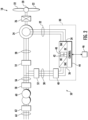
- FIG. 2 a schematic diagram of one embodiment of a DFIG wind turbine system 50 is illustrated in accordance with aspects of the present subject matter. It should be appreciated that the present subject matter will generally be described herein with reference to the system 50 shown in FIG. 2 . However, those of ordinary skill in the art, using the disclosures provided herein, should understand that aspects of the present disclosure may also be applicable in other power generation systems.
- the rotor 18 of the wind turbine 10 may, optionally, be coupled to a gear box 26, which is, in turn, coupled to the generator 24.
- the generator 24 is a doubly-fed induction generator (DFIG).
- the DFIG 24 may be coupled to a stator bus 28 and a power converter 30 via a rotor bus 32.
- the stator bus 28 may provide an output multiphase power (e.g., three-phase power) from a stator of the DFIG 24 and the rotor bus 32 may provide an output multiphase power (e.g., three-phase power) from a rotor of the DFIG 120.
- the power converter 30 includes a rotor side converter 34 and a line side converter 36.
- the DFIG 24 may be coupled via the rotor bus 32 to the rotor side converter 34.
- the rotor side converter 34 may be coupled to the line side converter 36 which may, in turn, be coupled to a line side bus 38.
- the power converter 30 may be a multi-level bridge power converter, such as a three-level bridge power converter, or higher.
- three-level converters are converters that have three direct current (DC) poles. In addition to positive and negative DC poles, such converters also have a neutral DC pole.
- the rotor side converter 34 and the line side converter 36 may be configured for normal operating mode in a three-phase, pulse width modulation (PWM) arrangement using insulated gate bipolar transistor (IGBT) switching devices.
- PWM pulse width modulation
- IGBT insulated gate bipolar transistor
- the rotor side converter 34 and the line side converter 36 may be coupled via a DC link 40 across which is a DC link capacitor 42.
- the power converter 30 may be coupled to a controller 44 in order to control the operation of the rotor side converter 34 and the line side converter 36.
- the controller 44 may, in several embodiments, be configured as an interface between the power converter 30 and a control system 46.
- the controller 44 may include any number of control devices.
- the controller 44 may include a processing device (e.g., microprocessor, microcontroller, etc.) executing computer-readable instructions stored in a computer-readable medium. The instructions when executed by the processing device may cause the processing device to perform operations, including providing control commands to the switching devices and/or the shorting devices of the power converter 30.
- various line contactors and circuit breakers including, for example, a grid breaker 62 may also be included for isolating the various components as necessary for normal operation of the DFIG 24 during connection to and disconnection from the electrical grid 64.
- a system circuit breaker 58 may couple the system bus 56 to a transformer 60, which may be coupled to the electrical grid 64 via the grid breaker 62.
- fuses may replace some or all of the circuit breakers.
- alternating current power generated at the DFIG 24 by rotating the rotor 18 is provided via a dual path to the electrical grid 64.
- the dual paths are defined by the stator bus 28 and the rotor bus 32.
- sinusoidal multi-phase (e.g., three-phase) alternating current (AC) power is provided to the power converter 30.
- the rotor side converter 34 converts the AC power provided from the rotor bus 32 into direct current (DC) power and provides the DC power to the DC link 40.
- switching devices e.g., IGBTs
- IGBTs used in the bridge circuits of the rotor side converter 34 may be modulated to convert the AC power provided from the rotor bus 32 into DC power suitable for the DC link 40.
- the line side converter 36 converts the DC power on the DC link 126 into AC output power suitable for the electrical grid 124.
- switching devices e.g., IGBTs
- IGBTs IGBTs
- the AC power from the power converter 30 can be combined with the power from the stator of DFIG 24 to provide multi-phase power (e.g., three-phase power) having a frequency maintained substantially at the frequency of the electrical grid 64 (e.g., 50 Hz or 60 Hz).
- circuit breakers and switches such as grid breaker 62, system breaker 58, stator sync switch 54, converter breaker 52, and line contactor 48 may be included in the system 50 to connect or disconnect corresponding buses, for example, when current flow is excessive and may damage components of the wind turbine 10 or for other operational considerations. Additional protection components may also be included in the DFIG wind turbine system 50, such as the crowbar circuit described below.
- the power converter 30 may receive control signals from, for instance, the control system 46 via the controller 44.
- the control signals may be based, among other things, on sensed conditions or operating characteristics of the DFIG wind turbine system 50.
- the control signals provide for control of the operation of the power converter 30.
- feedback in the form of a sensed speed of the DFIG 24 may be used to control the conversion of the output power from the rotor bus 32 to maintain a proper and balanced multi-phase (e.g., three-phase) power supply.
- Other feedback from other sensors may also be used by the controller 44 to control the power converter 30, including, for example, stator and rotor bus voltages and current feedbacks.
- switching control signals e.g., gate timing commands for IGBTs
- shorting control signals e.g., stator synchronizing control signals, and circuit breaker signals may be generated.
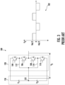
- FIG. 3 a schematic 100 of one leg 120 or one phase of a conventional neutral point clamped (NPC) or diode clamped three level converter and its output waveform 102 is illustrated.
- NPC neutral point clamped
- embodiments of the present disclosure enable a multi-level converter to convert DC power into an AC power with a switching device fault detection scheme.
- a switching device such as any of switching elements 104, 106, 108, or 110 of FIG. 3
- a clamping diode such as diodes 112 and 114 of FIG. 3
- the switching device failure detection scheme of the present disclosure provides a suitable logic circuit to detect failures in switching devices and so prevents secondary damage of multi-level converters which may be used in applications such as a solar (or photovoltaic) power generation systems, wind turbine generators or marine and hydrokinetic power generation systems.
- one leg 120 of the three-level converter includes four switching devices 104, 106, 108, 110 and two clamping diodes 112, 114.
- Input voltages V1 and V2 are controlled to each have a voltage equal to Vdc/2, where Vdc is the total DC link voltage.
- Voltage V3 is the phase A output voltage measured with respect to a center point 122 of DC link 124.
- Switching device 104 is complementary to switching device 108 so that, when switching device 104 is gated on, switching device 108 is gated off and vice versa.
- switching devices 106 and 110 are complementary.
- each leg of the NPC three-level converter has three switching stages.
- switching devices 104, 106 are turned on and switching devices 108, 110 are turned off.
- switching devices 106, 108 are turned on while switching devices 104, 110 are turned off.
- V3 is equal to zero.
- switching devices 104, 106 are turned off whereas switching devices 108, 110 are turned on. This results in V3 becoming -Vdc/2 as shown in waveform 102.
- the phase voltage V3 has three levels Vdc/2, -Vdc/2 and 0.
- the resulting line to line voltages have five levels namely Vdc, Vdc/2, 0, -Vdc/2 and -Vdc.
- the three-level converter of FIG. 3 may be increased to any level depending on the circuit topology and number of switching devices and diodes in the circuit. As the number of levels in the converter increases, the output waveform of the converter approaches a pure sine wave, resulting in lower harmonics in the output voltage. In general, the number of switching stages can be higher than three as switching devices may not be gated on if the corresponding free-wheeling diode is going to conduct current. This operation mode does not affect the number of levels of the output phase voltage.
- each leg 131 of the converter includes two outer switching devices (e.g., switching devices 134, 140) and four inner switching devices (e.g., switching devices 136, 138, 142, 144).
- outer switching devices e.g., switching devices 134, 140
- inner switching devices e.g., switching devices 136, 138, 142, 144
- the two outer switching devices e.g., switching devices 134, 140
- the four inner switching devices may also be referred to as a second IGBT, a third IGBT, a fifth IGBT, and a sixth IGBT.
- leg 131 is connected to a split DC link 150 with a top capacitor 152 and a bottom capacitor 154.
- FIG. 4 shows outer switching device 134 of leg 131 failing short (represented by referral numeral 132). The condition may occur as a result of occurrences such as, for example, thermal breakdown of outer switching device 134, the voltage breakdown of outer switching device 134, failures due to cosmic rays, and failures due to weak manufacturing of the switching device.
- the switching device failure detection circuit 160 includes logic modules or comparators 162, 164, 166, 168, 170, 172, each corresponding to a respective one of the switching devices 134, 136, 138, 140, 142, 144 ( FIG. 4 ).
- Switching device failure detection circuit 160 further includes a voltage calculation module 174, and a failure detection algorithm 176.
- each comparator 162, 164, 166, 168, 170, 172 compares two inputs, i) a switching device voltage i.e., a voltage across a switching device Vsw and ii) a threshold reference voltage Vth and provides an output voltage referred as blocking state logic signal Vc. Moreover, the following relationships exist between switching device voltage Vsw ( FIG. 5 ) and channel Ch ( FIG.
- Vsw 1 Ch 1 ⁇ Ch 2
- Vsw 2 Ch 6 ⁇ Ch 5
- Vsw 3 Ch 5
- Vsw 4 Ch 4
- Vsw 5 Ch 2
- Vsw 6 Ch 3 ⁇ Ch 4 ,
- Ch1 and Ch3 are Vdctop and Vdcbot,
- the threshold reference voltage Vth is set slightly higher than the rated voltage drop across the switching device when the switching device is conducting. In another embodiment, this signal is typically already available from de-saturation detection circuit, e.g., in IGBT converters. In yet another embodiment, the threshold reference voltage Vth may be set to an arbitrary suitable level between the voltage in the previous embodiment i.e., slightly higher than the rated voltage drop across the switching device and below the lower limit of Vdc/2. In another embodiment, the blocking state logic signal Vc is 'high' if Vsw is greater than Vth, else it is 'low'. It should be noted that 'high' refers to the positive supply voltage of the comparator and 'low' refers to the negative supply voltage of the comparator.
- comparator 162 compares Vsw1 and Vth and outputs Vc1, where Vsw1 refers to voltage across switching device 134, comparator 164 compares voltage across switching device 136, Vsw2 and Vth and outputs Vc2.
- comparator 166 compares Vsw3, which is voltage across switching device 138 and Vth, and outputs Vc3, comparator 168 compares voltage across switching device 140, Vsw4 and Vth and outputs Vc4, comparator 170 compares voltage across switching device 142, Vsw5 and Vth and outputs Vc5, and comparator 172 compares voltage across switching device 144, Vsw6 and Vth and outputs Vc6.
- the comparator(s) 162, 164, 166, 168, 170, 172 may be an open loop operational amplifier circuit or a dedicated voltage comparator integrated within a chip. In another embodiment, a portion of a desaturation circuit generally used in IGBT drivers, which provides a threshold voltage logic signal, may also be used as the comparator(s) 162, 164, 166, 168, 170, 172.
- the voltage calculation module 174 determines whether in the current switching stage, each switching device is supposed to block a voltage across its terminals or not.
- the output of the voltage calculation module 174 is the expected voltage (Vexp) for the switching devices that is input into switching device failure detection algorithm 176.
- An expected voltage (Vexp) at the output terminal points of leg 131 of the multi-level converter during normal condition is calculated as an intermediate step in voltage calculation module 174.
- the expected voltage is determined based on the inputs such as gate drive signals G1, G2, G3, G4, G5, G6 for switching devices 134, 136, 138, 140, 142, 144 and the corresponding output current direction, i.e., Io direction.
- the expected output voltage Vexp has three levels, positive, negative, and zero. Based on these levels, the gate drive signals, and the output current direction, the determination of whether a particular switching device should block the voltage or not is made and thus, the logic signals Vs1, Vs2, Vs3, Vs4, Vs5, and Vs6 are implicitly generated and used by the failure detection algorithm 176 (as shown in FIG. 7 ). If any of the logic signals is high, it indicates that the particular switching device should block the voltage, else it should not.
- the switching device failure detection algorithm 176 can then compare for each switching devices the information whether a switching device is actually blocking or not (i.e., Vc1, Vc2, Vc3, Vc4, Vc5, Vc6) with the information whether each device should be blocking or not (i.e., Vs1, Vs2, Vs3, Vs4, Vs5, and Vs6) in the current switching stage. If actual blocking state and expected blocking state of any switching device do not match (for example if Vc1 ⁇ Vs1), a failure is detected.
- the above switching device failure detection circuit 160 may be implemented in the analog domain, or the digital domain, or a combination thereof.
- the circuitry can generally include analog-to-digital conversion, although analog processing components may generally not require such conversion unless some processing is done in the digital domain.
- Examples of digital circuitry include digital components, such as a programmed microprocessor, field programmable gate array (FPGA), application specific digital signal processor (DSP) or the like. It should be noted that the particular order of processing as represented by the components shown in FIG. 5 may be altered, and other components may be included in the overall circuitry, where desired.
- the voltage calculation module 180 receives inputs such as gate drive signals G1, G2, G3, G4, G5, G6 for switching devices 134, 136, 138, 140, 142, 144, respectively, and also output current or Io direction.
- the gate drive signal levels determine whether any switching device is ON or not. For example, if G2 or G3 is high, switching devices 136 and 138 are ON, respectively. Thus, for all the cases presented below, if the switching device is ON, the corresponding gate drive signal is referred to as high.
- the gate drive signals (i.e., G1, G2, and G4) for the first IGBT, the third IGBT, and the fourth IGBT are low, the gate drive signal (G2) for the second IGBT is high, the output current direction is negative, and the gate signals (i.e., G5, G6) of the fifth IGBT and the sixth IGBT are high, then as shown at 186, the expected output voltage is a zero voltage.
- the gate drive signals i.e., G1, G3, and G4
- the gate drive signal (G2) of the second IGBT is high
- the output current direction is negative
- the gate drivel signals (i.e., G5, G6) for the fifth IGBT or the sixth IGBT are low, then as shown at 184, the expected output voltage is a positive voltage.
- the gate drive signals i.e., G1, G2, and G4
- the gate drive signal (G3) of the third IGBT is high
- the output current direction is positive
- the gate signals (i.e., G5, G6) of the fifth IGBT and the sixth IGBT are high, then as shown at 191, the expected output voltage is a zero voltage.
- the gate drive signals i.e., G1, G2, and G4
- the gate drive signal (G3) of the third IGBT is high
- the output current direction is positive
- the gate drivel signals (i.e., G5, G6) for the fifth IGBT or the sixth IGBT are low, then as shown at 190, the expected output voltage is a negative voltage.
- step 192 it can be further determined whether any one of inner switching devices 136, 138 (e.g., second IGBT or third IGBT) are ON and whether both outer switching devices 134, 140 (e.g., first IGBT or fourth IGBT) are OFF.
- the expected voltage Vexp is equivalent to a zero voltage as represented by a block 193.
- both top switching devices 134, 136 e.g., first IGBT and second IGBT
- Both bottom switching devices 138, 140 being ON indicates that expected voltage Vexp should be a negative voltage i.e., V- represented by a block 201. If any of the conditions 192, 194, 195 are not met, then the output current (Io) direction helps in determining the expected voltage Vexp, as shown at 196 and 199.
- the expected voltage Vexp during this condition will be positive voltage V+, as represented by block 198. If it is determined at 196, that output current Io is not negative (i.e., positive or zero), then as shown at 199, it is determined whether the output current Io is positive or not. If the output current Io is positive, as shown at 200, it is again determined whether the switching devices 134, 136, 138, 140 are OFF. If the switching devices 134, 136, 138, 140 are OFF and the current direction is positive, it indicates that freewheeling diodes of the bottom two switching devices (e.g., third IGBT or fourth IGBT) are conducting and the expected voltage during this condition will be negative voltage V-(as shown at 201).
- the switching devices 134, 136, 138, 140 are OFF and the current direction is positive, it indicates that freewheeling diodes of the bottom two switching devices (e.g., third IGBT or fourth IGBT) are conducting and the expected voltage during this condition will be negative voltage V-
- the failure detection algorithm 210 determines whether any switching device that should block a DC voltage is actually not blocking DC voltage. In particular, as shown at 212, it is determined whether expected voltage Vexp is positive (V+) or not. If Vexp is not equal to V+, i.e., if Vexp is equal to negative voltage V- or zero voltage, then as shown at 214, it is checked whether blocking state logic signal Vc1 of first switching device 134 is low or high. If Vc1 is low then it indicates that switching device 134 is not blocking any voltage when actually it should block the voltage.
- Vexp is negative voltage i.e., V-. If it is determined at 218 that Vexp is indeed V-, then as shown at 220, it is checked whether blocking state logic signal Vc2 for switching device 136 is low. If Vc2 is low, then the second switching device 136 is considered to be faulty as shown in block 222. If it is determined that Vexp is a positive voltage i.e., V+, then as shown at 224, the blocking state logic signal Vc3 for switching device 138 is compared with the low voltage. If it is found that Vc3 is low, then it means the switching device 138 is faulty as shown in block 226.
- the blocking state logic signal Vc4 for the switching device 138 is low. If Vc4 is low, then it is indication of the switching device 140 being faulty as shown in block 230. Moreover, if it is determined that Vexp is a positive voltage i.e., V+, then as shown at 236, the blocking state logic signal Vc5 for switching device 142 is compared with the low voltage. If it is found that Vc5 is low, then it means the switching device 142 is faulty as shown in block 238.
- Vexp is a negative voltage i.e., V-
- the blocking state logic signal Vc6 for switching device 144 is compared with the low voltage. If it is found that Vc6 is low, then it means the switching device 144 is faulty as shown in block 234. Thus, in this way with various combinations, failure conditions of switching devices are determined.
- steps presented in FIGS. 6 and 7 are not restricted by their sequence. For instance, in an embodiment, some of the steps can be performed in parallel or in another embodiment; the sequence of the steps can be interchanged as long as it does not affect the final outcome.
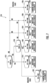
- FIG. 8 a flow diagram of one embodiment of a computer-implemented method 300 for operating a multi-level bridge power converter of an electrical power system connected to a power grid is illustrated in accordance with aspects of the present subject matter.
- the method 300 will be described herein as being implemented using a wind turbine system, such as the DFIG wind turbine system 50 described above with reference to FIGS. 1-7 .
- the disclosed method 300 may be implemented using any other suitable power generation system that is configured to supply power for application to a load.
- FIG. 8 depicts steps performed in a particular order for purposes of illustration and discussion, the methods described herein are not limited to any particular order or arrangement.
- steps of the methods can be omitted, rearranged, combined and/or adapted in various ways.
- the method 300 includes arranging a plurality of switching devices having at least four inner switching devices and at least two outer switching devices in an active neutral point clamped topology. As shown at (304), the method 300 includes determining whether any of the plurality of switching devices is experiencing a failure condition by implementing a failure detection algorithm. As shown at (306), the failure detection algorithm includes generating a blocking state logic signal by comparing a switching device voltage and a threshold reference voltage for each of the plurality of switching devices. As shown at (308), the failure detection algorithm includes determining an expected voltage blocking state for each of the plurality of switching devices based on gate drive signals of the plurality of switching devices and an output current direction. As shown at (310), the failure detection algorithm includes detecting whether a failure condition is present in any of the plurality of switching devices based on the blocking state logic signals and the expected voltage blocking states of the plurality of switching devices.
Landscapes
- Engineering & Computer Science (AREA)
- Power Engineering (AREA)
- Physics & Mathematics (AREA)
- General Physics & Mathematics (AREA)
- Microelectronics & Electronic Packaging (AREA)
- Inverter Devices (AREA)
Applications Claiming Priority (1)
| Application Number | Priority Date | Filing Date | Title |
|---|---|---|---|
| US17/534,507 US11923783B2 (en) | 2021-11-24 | 2021-11-24 | System and method for detection of switching device failure conditions in a multi-level power converter |
Publications (1)
| Publication Number | Publication Date |
|---|---|
| EP4187766A1 true EP4187766A1 (de) | 2023-05-31 |
Family
ID=84330070
Family Applications (1)
| Application Number | Title | Priority Date | Filing Date |
|---|---|---|---|
| EP22205840.6A Pending EP4187766A1 (de) | 2021-11-24 | 2022-11-07 | System und verfahren zur erkennung von schaltvorrichtungsausfallzuständen in einem mehrstufigen stromwandler |
Country Status (3)
| Country | Link |
|---|---|
| US (1) | US11923783B2 (de) |
| EP (1) | EP4187766A1 (de) |
| CN (1) | CN116165526A (de) |
Families Citing this family (2)
| Publication number | Priority date | Publication date | Assignee | Title |
|---|---|---|---|---|
| US12244244B2 (en) * | 2022-04-28 | 2025-03-04 | General Electric Renovables Espana, S.L. | Fault tolerant system and method for continuous skip-fire pulse width modulation for an active neutral point clamped converter |
| DE102024200624A1 (de) * | 2024-01-24 | 2025-01-02 | Zf Friedrichshafen Ag | Wechselrichter, Verfahren und Vorrichtung zum Betreiben eines Wechselrichters |
Citations (3)
| Publication number | Priority date | Publication date | Assignee | Title |
|---|---|---|---|---|
| US20070159749A1 (en) * | 2006-01-10 | 2007-07-12 | Toshiba Mitsubishi-Electric Indus. Sys.Corp. | Multi-level power converter |
| EP2393198A2 (de) * | 2010-05-28 | 2011-12-07 | General Electric Company | System zur Detektion von Schaltvorrichtungsfehlern und Verfahren für mehrstufige Wandler |
| US10063161B2 (en) * | 2016-10-18 | 2018-08-28 | Abb Schweiz Ag | Active neutral point clamped converter control system and method |
Family Cites Families (5)
| Publication number | Priority date | Publication date | Assignee | Title |
|---|---|---|---|---|
| US8207736B2 (en) | 2009-09-30 | 2012-06-26 | General Electric Company | Apparatus for feeding a magnetic resonance coil element and method of making same |
| US8472153B1 (en) | 2011-12-20 | 2013-06-25 | General Electric Company | Neutral point clamped power converter fault detection, identification, and protection |
| CN103378759B (zh) | 2012-04-19 | 2017-04-05 | 马文忠 | 一种npc三电平逆变器故障冗余控制方法 |
| US20160352251A1 (en) | 2015-05-31 | 2016-12-01 | Abb Technology Ag | Active Neutral-Point-Clamped (ANPC) Converters and Operating Methods Thereof |
| CN106877720B (zh) | 2017-04-28 | 2019-03-05 | 阳光电源股份有限公司 | 有源中点钳位型逆变器及其过零切换方法和过零切换装置 |
-
2021
- 2021-11-24 US US17/534,507 patent/US11923783B2/en active Active
-
2022
- 2022-11-07 EP EP22205840.6A patent/EP4187766A1/de active Pending
- 2022-11-24 CN CN202211487449.6A patent/CN116165526A/zh active Pending
Patent Citations (3)
| Publication number | Priority date | Publication date | Assignee | Title |
|---|---|---|---|---|
| US20070159749A1 (en) * | 2006-01-10 | 2007-07-12 | Toshiba Mitsubishi-Electric Indus. Sys.Corp. | Multi-level power converter |
| EP2393198A2 (de) * | 2010-05-28 | 2011-12-07 | General Electric Company | System zur Detektion von Schaltvorrichtungsfehlern und Verfahren für mehrstufige Wandler |
| US10063161B2 (en) * | 2016-10-18 | 2018-08-28 | Abb Schweiz Ag | Active neutral point clamped converter control system and method |
Non-Patent Citations (1)
| Title |
|---|
| FRANCOIS B ET AL: "Design of a fault tolerant control system for a N.P.C. multilevel inverter", INDUSTRIAL ELECTRONICS, 2002. ISIE 2002. PROCEEDINGS OF THE 2002 IEEE INTERNATIONAL SYMPOSIUM ON JULY 8-11, 2002, PISCATAWAY, NJ, USA,IEEE, vol. 4, 8 July 2002 (2002-07-08), pages 1075 - 1080, XP010598076, ISBN: 978-0-7803-7369-3 * |
Also Published As
| Publication number | Publication date |
|---|---|
| US11923783B2 (en) | 2024-03-05 |
| US20230163695A1 (en) | 2023-05-25 |
| CN116165526A (zh) | 2023-05-26 |
Similar Documents
| Publication | Publication Date | Title |
|---|---|---|
| EP2383878B1 (de) | System und Verfahren zum Schutz eines mehrstufigen Wandlers | |
| US8471584B2 (en) | Switching device failure detection system and method for multilevel converters | |
| US9140744B2 (en) | Doubly-fed induction generator system and the self-test method for the active crowbar circuit thereof | |
| US10530152B2 (en) | Power distribution systems | |
| EP2771956A1 (de) | Schnittstellenanordnung zwischen ac- und dc-systemen zur zuverlässigen zeitgerechten öffnung eines schutzschalters | |
| EP4187766A1 (de) | System und verfahren zur erkennung von schaltvorrichtungsausfallzuständen in einem mehrstufigen stromwandler | |
| US20200158085A1 (en) | Power converter for full conversion wind turbine systems | |
| EP4266580A1 (de) | System und verfahren zur erkennung von igbt-fehlern in einem mehrstufigen wandler mit gate-emitter-spannungserfassung | |
| US9455568B2 (en) | Energy storage system for renewable energy source | |
| EP3961886A1 (de) | Überspannungsmodul für eine aktive leistungswandleranordnung mit nullpunktklemmung | |
| EP4057494A1 (de) | Aktive neutralpunktspannungsschaltfolge zur parasitären induktivitätssteuerung eines leistungsumwandlungssystems | |
| US11594953B1 (en) | System and method for operating multi-level power converter using a multi-state deadtime | |
| EP4270750A1 (de) | Fehlertolerantes system und verfahren zur kontinuierlichen skip-fire-pulsweitenmodulation für einen aktiven neutralpunktgeklemmten wandler | |
| Li et al. | Application of active NPC converter on generator side for MW direct-driven wind turbine | |
| EP4138292A1 (de) | System und verfahren zum betrieb eines mehrstufigen leistungswandlers mit mehreren totzeiten | |
| US12255572B1 (en) | System and method for detecting a stator distortion filter in an electrical power system | |
| Bhakar et al. | A New Fault-Tolerant Method for Switch Failures in Three-Phase Inverter | |
| Lažek et al. | Simulation of Fault Operation of a 13-level CHB Multilevel Converter for Power Coolant Pump | |
| Li | Design, control and characteristics of multilevel active NPC converters for high power applications |
Legal Events
| Date | Code | Title | Description |
|---|---|---|---|
| PUAI | Public reference made under article 153(3) epc to a published international application that has entered the european phase |
Free format text: ORIGINAL CODE: 0009012 |
|
| STAA | Information on the status of an ep patent application or granted ep patent |
Free format text: STATUS: THE APPLICATION HAS BEEN PUBLISHED |
|
| AK | Designated contracting states |
Kind code of ref document: A1 Designated state(s): AL AT BE BG CH CY CZ DE DK EE ES FI FR GB GR HR HU IE IS IT LI LT LU LV MC ME MK MT NL NO PL PT RO RS SE SI SK SM TR |
|
| STAA | Information on the status of an ep patent application or granted ep patent |
Free format text: STATUS: REQUEST FOR EXAMINATION WAS MADE |
|
| 17P | Request for examination filed |
Effective date: 20231122 |
|
| RBV | Designated contracting states (corrected) |
Designated state(s): AL AT BE BG CH CY CZ DE DK EE ES FI FR GB GR HR HU IE IS IT LI LT LU LV MC ME MK MT NL NO PL PT RO RS SE SI SK SM TR |