EP4197766A1 - Verfahren zum mikroformen von mikrostrukturierten folien und linsen - Google Patents
Verfahren zum mikroformen von mikrostrukturierten folien und linsen Download PDFInfo
- Publication number
- EP4197766A1 EP4197766A1 EP21306818.2A EP21306818A EP4197766A1 EP 4197766 A1 EP4197766 A1 EP 4197766A1 EP 21306818 A EP21306818 A EP 21306818A EP 4197766 A1 EP4197766 A1 EP 4197766A1
- Authority
- EP
- European Patent Office
- Prior art keywords
- forming
- microstructures
- thermoforming
- forming insert
- insert
- Prior art date
- Legal status (The legal status is an assumption and is not a legal conclusion. Google has not performed a legal analysis and makes no representation as to the accuracy of the status listed.)
- Pending
Links
- 238000000034 method Methods 0.000 title claims abstract description 53
- 238000003856 thermoforming Methods 0.000 claims abstract description 52
- 230000003287 optical effect Effects 0.000 claims abstract description 45
- 238000010438 heat treatment Methods 0.000 claims abstract description 20
- 239000002861 polymer material Substances 0.000 claims abstract description 4
- 239000000463 material Substances 0.000 claims description 10
- 238000012546 transfer Methods 0.000 claims description 5
- 238000003825 pressing Methods 0.000 claims description 3
- 235000012431 wafers Nutrition 0.000 description 63
- 239000010408 film Substances 0.000 description 15
- 238000000386 microscopy Methods 0.000 description 12
- 238000000879 optical micrograph Methods 0.000 description 12
- 230000008569 process Effects 0.000 description 7
- 239000011521 glass Substances 0.000 description 6
- 239000000758 substrate Substances 0.000 description 5
- 238000004519 manufacturing process Methods 0.000 description 4
- 230000004379 myopia Effects 0.000 description 4
- 208000001491 myopia Diseases 0.000 description 4
- 238000012545 processing Methods 0.000 description 4
- 206010020675 Hypermetropia Diseases 0.000 description 3
- 238000013461 design Methods 0.000 description 3
- 230000004305 hyperopia Effects 0.000 description 3
- 201000006318 hyperopia Diseases 0.000 description 3
- 238000001746 injection moulding Methods 0.000 description 3
- 238000000465 moulding Methods 0.000 description 3
- 239000012788 optical film Substances 0.000 description 3
- 229920000515 polycarbonate Polymers 0.000 description 3
- 239000004417 polycarbonate Substances 0.000 description 3
- 229910001220 stainless steel Inorganic materials 0.000 description 3
- 239000010935 stainless steel Substances 0.000 description 3
- NNLVGZFZQQXQNW-ADJNRHBOSA-N [(2r,3r,4s,5r,6s)-4,5-diacetyloxy-3-[(2s,3r,4s,5r,6r)-3,4,5-triacetyloxy-6-(acetyloxymethyl)oxan-2-yl]oxy-6-[(2r,3r,4s,5r,6s)-4,5,6-triacetyloxy-2-(acetyloxymethyl)oxan-3-yl]oxyoxan-2-yl]methyl acetate Chemical compound O([C@@H]1O[C@@H]([C@H]([C@H](OC(C)=O)[C@H]1OC(C)=O)O[C@H]1[C@@H]([C@@H](OC(C)=O)[C@H](OC(C)=O)[C@@H](COC(C)=O)O1)OC(C)=O)COC(=O)C)[C@@H]1[C@@H](COC(C)=O)O[C@@H](OC(C)=O)[C@H](OC(C)=O)[C@H]1OC(C)=O NNLVGZFZQQXQNW-ADJNRHBOSA-N 0.000 description 2
- 238000001816 cooling Methods 0.000 description 2
- 239000002537 cosmetic Substances 0.000 description 2
- 238000005520 cutting process Methods 0.000 description 2
- 238000004049 embossing Methods 0.000 description 2
- 238000005516 engineering process Methods 0.000 description 2
- 230000004438 eyesight Effects 0.000 description 2
- ZZUFCTLCJUWOSV-UHFFFAOYSA-N furosemide Chemical compound C1=C(Cl)C(S(=O)(=O)N)=CC(C(O)=O)=C1NCC1=CC=CO1 ZZUFCTLCJUWOSV-UHFFFAOYSA-N 0.000 description 2
- 230000009477 glass transition Effects 0.000 description 2
- 238000002347 injection Methods 0.000 description 2
- 239000007924 injection Substances 0.000 description 2
- 238000012986 modification Methods 0.000 description 2
- 230000004048 modification Effects 0.000 description 2
- 238000001314 profilometry Methods 0.000 description 2
- 210000001747 pupil Anatomy 0.000 description 2
- 229920001169 thermoplastic Polymers 0.000 description 2
- 239000004416 thermosoftening plastic Substances 0.000 description 2
- 229920002284 Cellulose triacetate Polymers 0.000 description 1
- 229920000089 Cyclic olefin copolymer Polymers 0.000 description 1
- 239000004713 Cyclic olefin copolymer Substances 0.000 description 1
- 241001142635 Lema Species 0.000 description 1
- 229940081735 acetylcellulose Drugs 0.000 description 1
- 229920006397 acrylic thermoplastic Polymers 0.000 description 1
- 239000000853 adhesive Substances 0.000 description 1
- 230000001070 adhesive effect Effects 0.000 description 1
- 229920006020 amorphous polyamide Polymers 0.000 description 1
- 230000015572 biosynthetic process Effects 0.000 description 1
- 229920002678 cellulose Polymers 0.000 description 1
- 229920002301 cellulose acetate Polymers 0.000 description 1
- 229920006217 cellulose acetate butyrate Polymers 0.000 description 1
- 238000004140 cleaning Methods 0.000 description 1
- 238000010276 construction Methods 0.000 description 1
- 238000012937 correction Methods 0.000 description 1
- 230000001419 dependent effect Effects 0.000 description 1
- 229910003460 diamond Inorganic materials 0.000 description 1
- 239000010432 diamond Substances 0.000 description 1
- 238000007516 diamond turning Methods 0.000 description 1
- 238000003475 lamination Methods 0.000 description 1
- 238000005259 measurement Methods 0.000 description 1
- 239000002086 nanomaterial Substances 0.000 description 1
- 230000037361 pathway Effects 0.000 description 1
- 229920003229 poly(methyl methacrylate) Polymers 0.000 description 1
- 229920006289 polycarbonate film Polymers 0.000 description 1
- -1 polyethylene terephthalate Polymers 0.000 description 1
- 229920000139 polyethylene terephthalate Polymers 0.000 description 1
- 239000005020 polyethylene terephthalate Substances 0.000 description 1
- 229920000306 polymethylpentene Polymers 0.000 description 1
- 239000011116 polymethylpentene Substances 0.000 description 1
- 239000011148 porous material Substances 0.000 description 1
- 230000002265 prevention Effects 0.000 description 1
- 230000004515 progressive myopia Effects 0.000 description 1
- 230000001681 protective effect Effects 0.000 description 1
- 230000009467 reduction Effects 0.000 description 1
- 239000000243 solution Substances 0.000 description 1
- ISXSCDLOGDJUNJ-UHFFFAOYSA-N tert-butyl prop-2-enoate Chemical compound CC(C)(C)OC(=O)C=C ISXSCDLOGDJUNJ-UHFFFAOYSA-N 0.000 description 1
- 230000000930 thermomechanical effect Effects 0.000 description 1
- 229920001187 thermosetting polymer Polymers 0.000 description 1
Images




Classifications
-
- B—PERFORMING OPERATIONS; TRANSPORTING
- B29—WORKING OF PLASTICS; WORKING OF SUBSTANCES IN A PLASTIC STATE IN GENERAL
- B29C—SHAPING OR JOINING OF PLASTICS; SHAPING OF MATERIAL IN A PLASTIC STATE, NOT OTHERWISE PROVIDED FOR; AFTER-TREATMENT OF THE SHAPED PRODUCTS, e.g. REPAIRING
- B29C51/00—Shaping by thermoforming, i.e. shaping sheets or sheet like preforms after heating, e.g. shaping sheets in matched moulds or by deep-drawing; Apparatus therefor
- B29C51/26—Component parts, details or accessories; Auxiliary operations
- B29C51/30—Moulds
- B29C51/36—Moulds specially adapted for vacuum forming, Manufacture thereof
-
- B—PERFORMING OPERATIONS; TRANSPORTING
- B29—WORKING OF PLASTICS; WORKING OF SUBSTANCES IN A PLASTIC STATE IN GENERAL
- B29D—PRODUCING PARTICULAR ARTICLES FROM PLASTICS OR FROM SUBSTANCES IN A PLASTIC STATE
- B29D11/00—Producing optical elements, e.g. lenses or prisms
- B29D11/00009—Production of simple or compound lenses
- B29D11/0048—Moulds for lenses
-
- B—PERFORMING OPERATIONS; TRANSPORTING
- B29—WORKING OF PLASTICS; WORKING OF SUBSTANCES IN A PLASTIC STATE IN GENERAL
- B29C—SHAPING OR JOINING OF PLASTICS; SHAPING OF MATERIAL IN A PLASTIC STATE, NOT OTHERWISE PROVIDED FOR; AFTER-TREATMENT OF THE SHAPED PRODUCTS, e.g. REPAIRING
- B29C51/00—Shaping by thermoforming, i.e. shaping sheets or sheet like preforms after heating, e.g. shaping sheets in matched moulds or by deep-drawing; Apparatus therefor
- B29C51/10—Forming by pressure difference, e.g. vacuum
-
- B—PERFORMING OPERATIONS; TRANSPORTING
- B29—WORKING OF PLASTICS; WORKING OF SUBSTANCES IN A PLASTIC STATE IN GENERAL
- B29D—PRODUCING PARTICULAR ARTICLES FROM PLASTICS OR FROM SUBSTANCES IN A PLASTIC STATE
- B29D11/00—Producing optical elements, e.g. lenses or prisms
- B29D11/00009—Production of simple or compound lenses
-
- B—PERFORMING OPERATIONS; TRANSPORTING
- B29—WORKING OF PLASTICS; WORKING OF SUBSTANCES IN A PLASTIC STATE IN GENERAL
- B29D—PRODUCING PARTICULAR ARTICLES FROM PLASTICS OR FROM SUBSTANCES IN A PLASTIC STATE
- B29D11/00—Producing optical elements, e.g. lenses or prisms
- B29D11/00009—Production of simple or compound lenses
- B29D11/00317—Production of lenses with markings or patterns
- B29D11/00326—Production of lenses with markings or patterns having particular surface properties, e.g. a micropattern
-
- B—PERFORMING OPERATIONS; TRANSPORTING
- B29—WORKING OF PLASTICS; WORKING OF SUBSTANCES IN A PLASTIC STATE IN GENERAL
- B29D—PRODUCING PARTICULAR ARTICLES FROM PLASTICS OR FROM SUBSTANCES IN A PLASTIC STATE
- B29D11/00—Producing optical elements, e.g. lenses or prisms
- B29D11/00009—Production of simple or compound lenses
- B29D11/00432—Auxiliary operations, e.g. machines for filling the moulds
-
- B—PERFORMING OPERATIONS; TRANSPORTING
- B29—WORKING OF PLASTICS; WORKING OF SUBSTANCES IN A PLASTIC STATE IN GENERAL
- B29C—SHAPING OR JOINING OF PLASTICS; SHAPING OF MATERIAL IN A PLASTIC STATE, NOT OTHERWISE PROVIDED FOR; AFTER-TREATMENT OF THE SHAPED PRODUCTS, e.g. REPAIRING
- B29C59/00—Surface shaping of articles, e.g. embossing; Apparatus therefor
- B29C59/02—Surface shaping of articles, e.g. embossing; Apparatus therefor by mechanical means, e.g. pressing
- B29C59/022—Surface shaping of articles, e.g. embossing; Apparatus therefor by mechanical means, e.g. pressing characterised by the disposition or the configuration, e.g. dimensions, of the embossments or the shaping tools therefor
- B29C2059/023—Microembossing
-
- B—PERFORMING OPERATIONS; TRANSPORTING
- B29—WORKING OF PLASTICS; WORKING OF SUBSTANCES IN A PLASTIC STATE IN GENERAL
- B29C—SHAPING OR JOINING OF PLASTICS; SHAPING OF MATERIAL IN A PLASTIC STATE, NOT OTHERWISE PROVIDED FOR; AFTER-TREATMENT OF THE SHAPED PRODUCTS, e.g. REPAIRING
- B29C51/00—Shaping by thermoforming, i.e. shaping sheets or sheet like preforms after heating, e.g. shaping sheets in matched moulds or by deep-drawing; Apparatus therefor
-
- B—PERFORMING OPERATIONS; TRANSPORTING
- B29—WORKING OF PLASTICS; WORKING OF SUBSTANCES IN A PLASTIC STATE IN GENERAL
- B29L—INDEXING SCHEME ASSOCIATED WITH SUBCLASS B29C, RELATING TO PARTICULAR ARTICLES
- B29L2011/00—Optical elements, e.g. lenses, prisms
-
- B—PERFORMING OPERATIONS; TRANSPORTING
- B29—WORKING OF PLASTICS; WORKING OF SUBSTANCES IN A PLASTIC STATE IN GENERAL
- B29L—INDEXING SCHEME ASSOCIATED WITH SUBCLASS B29C, RELATING TO PARTICULAR ARTICLES
- B29L2011/00—Optical elements, e.g. lenses, prisms
- B29L2011/0016—Lenses
Definitions
- the present disclosure relates to a method for fabricating microstructured films or microstructured lenses by a micro-forming or micro-embossing.
- Injection molding of lenses can use glass inserts having microlenses on their surface that are difficult to produce on typical glass materials such as borosilicate. That is, forming microstructures on a glass surface can be expensive, difficult to produce, can lead to glass breakage during microstructure engraving, and are easily and often broken during handling, cleaning, and in the production of lenses. Moreover, glass inserts break easily during injection molding, which leads to significant equipment down time and thus reduces yields and productivity.
- NiP coated stainless steel mold inserts can be used to remedy some challenges of glass inserts.
- NiP coated stainless steel mold inserts can also be expensive to produce, customized for a single base curve lens, replaced yearly or when damaged, and entail long lead times for fabrication.
- lenses or wafers with microlenses on the surface that are made from diamond turned NiP coated stainless steel mold inserts can have the risk of cosmetics issues such as tooling marks, swirls, channels, melt weld-lines, center distortion, and cosmetic or optical deformations.
- the present disclosure relates to a method of forming an optical element, including: providing a forming insert in a thermoforming apparatus, the forming insert including a plurality of microstructures formed on a forming surface of the forming insert; heating the forming insert to a first predetermined temperature; disposing an element comprised of a polymer material in the thermoforming apparatus and in contact with the forming surface of the forming insert; and thermoforming, via the forming surface of the forming insert, the element, the molded element having microstructures formed on a surface thereof.
- the present disclosure relates to a method as disclosed in claim 1. Advantageous aspects of the method according to the present disclosure are disclosed in claims 2 to 13.
- the present disclosure additionally relates to a thermoforming apparatus, comprising: a forming insert including a plurality of microstructures formed on a forming surface thereof; a heating element heating the forming insert to a first predetermined temperature; and a pressure system, a vacuum system, and/or mechanical force system that supports thermoforming of an element to form microstructures on a surface thereof by applying a pressure, a vacuum suction and/or a mechanical force to an element in contact with the forming surface of the forming insert.
- the present disclosure additionally relates to a thermoforming apparatus as disclosed in claim 14. Advantageous aspects of the thermoforming apparatus according to the present disclosure are disclosed in claim 15.
- first and second features are formed in direct contact
- additional features may be formed between the first and second features, such that the first and second features may not be in direct contact
- present disclosure may repeat reference numerals and/or letters in the various examples.
- spatially relative terms such as “top,” “bottom,” “beneath,” “below,” “lower,” “above,” “upper” and the like, may be used herein for ease of description to describe one element or feature's relationship to another element(s) or feature(s) as illustrated in the figures.
- the spatially relative terms are intended to encompass different orientations of the device in use or operation in addition to the orientation depicted in the figures.
- Inventive apparatuses may be otherwise oriented (rotated 90 degrees or at other orientations) and the spatially relative descriptors used herein may likewise be interpreted accordingly.
- thermoforming in many ways has the ability to replicate very fine and intricate geometries while also changing the geometry of a substrate at the same time. This is particularly useful in ophthalmic applications where various degrees of curvatures can be produced to address issues pertaining to vision correction.
- a process leveraging a thermoforming apparatus having a pattern formed therein can be used.
- a method to fabricate microstructured films or microstructured lenses uses a microforming or microembossing technique.
- a heated forming insert can be used to produce raised or recessed microstructures on film, semi-finished, or finished single vision polycarbonate lenses for myopia control and myopia prevention.
- the method includes heating the surface that is in contact with the forming insert to above a deformation temperature (i.e., a glass transition temperature, T g ) of the material (for example, 10°C to 20°C above the T g ) and either applying pressure, vacuum, or mechanical force to the film or lens.
- a deformation temperature i.e., a glass transition temperature, T g
- T g glass transition temperature
- thermoforming i.e., the microforming or the microembossing
- the thermoforming technique can be plug-assisted forming, hydro-assisted forming, pressure-assisted forming, or vacuum-assisted forming.
- the disclosed method can create a pathway to modify the thermoforming process via the addition of micron-scale cavities or raised/recessed structures onto a thermoforming apparatus to impregnate optical films with microstructures of different size, shapes, and periodicities.
- this single-step process can reduce the cost of preparing microlens films. Large scale micro thermoforming processes could open up the possibility of producing inexpensive lenses due to a reduction in processing steps.
- Die cutting tools can be used to cut wafers from flat film or laminate sheets into circular or oval disks. These flat laminate wafers are then thermoformed into a spherical dome shape.
- the diameter of the flat laminate wafers are determined by considering, at least, one or more of: the desired lens diameter (e.g., 70 mm, 76 mm, 80 mm, etc.), the base curve of the thermoformed wafer (e.g., 0.25, 1.75, 3.00, 4.00, 4.50, 5.50, 6.00, 6.50, 7.25, 8.00 Diopters, etc.), and the base curve of the mold insert (e.g., 1.75, 2.25, 3.25, 4.25, 5.50, 6.50, 7.50, 8.50 Diopters, etc.).
- the base curve of the mold insert can be the same base curve as the convex power surface of the lens.
- FIG. 1A is a schematic of a flat wafer 100, useful within the scope of the present disclosure.
- the flat wafer 100 can be any optical element or optical material formed into a structure for thermoforming.
- Materials for the flat wafer 100 or optical element include polycarbonate, cellulose esters (e.g., cellulose triacetate, cellulose acetate proprionate, cellulose acetate butyrate), acrylics, cyclic olefin copolymers, amorphous polyamides, polyethylene-naphthalene, polyethylene terephthalate, polymethyl-pentene, and the like, and optically transparent film/laminate with little to no haze.
- FIG. 1A is a schematic of a flat wafer 100, useful within the scope of the present disclosure.
- the flat wafer 100 can be any optical element or optical material formed into a structure for thermoforming.
- Materials for the flat wafer 100 or optical element include polycarbonate, cellulose esters (e.g., cellulose triacetate,
- the flat wafer 100 can be circular or elliptical.
- a diameter, d fw of a circular flat wafer is the same length as an arc length of a thermoformed wafer 105 (see FIG. 1B ) after thermoforming.
- an elliptical flat wafer 100 can include a semimajor axis, d fw1 , and a semiminor axis, dfw2.
- FIG. 1B is a schematic of the thermoformed wafer 105, useful within the scope of the present disclosure.
- a cord length, d TF of the thermoformed wafer 105 can be approximately the same diameter as a diameter of the lens.
- the flat wafer 100 need not be flat before being thermoformed.
- a wafer having a low base curvature can be formed via thermoforming, then thermoformed again to produce a wafer having a higher base curvature.
- FIG. 1C is a schematic of a concave mold insert 130, useful within the scope of the present disclosure.
- the diameter of the lens can be determined by, for example, a diameter, d Insert , of the concave mold insert 130.
- both the chord length ( d TF ) and the concave mold insert 130 diameter ( d Insert ) can be smaller in diameter than the diameter ( d fw ) of the flat wafer 100.
- the arc length of the concave mold insert 130 can be equal to or greater than the arc length ( d fw ) of the thermoformed laminate wafer 105 due to the differences in the base curves of the flat wafer 100 and the concave mold insert 130.
- FIG. 2 is a schematic of a thermoforming apparatus 200, useful within the scope of the present disclosure.
- the thermoforming apparatus 200 can include a forming insert 210 having a forming surface 215, the forming surface 215 including concave or convex microstructures 205 formed thereon, wherein in one example, the inverted/concave microstructures 205 are microcavities (as shown).
- the (convex/concave) microstructures 205 can instead be microprotrusions, microindentations, microperforations, or any combination of the aforementioned microstructural features.
- the forming surface 215 of the forming insert 210 can have a curvature (as well as the forming insert 210) and the microstructures 205 can be formed along the curvature of the forming surface 215.
- the forming surface 215 is concave (as shown).
- the forming surface 215 is convex.
- the thermoforming apparatus 200, including the forming insert 210, can be heated to a predetermined temperature based on a glass transition temperature of the flat wafer 100.
- the flat wafer 100 can be disposed within the thermoforming apparatus 200 and in contact with the forming surface 215 of the forming insert 210.
- a force can be applied to the flat wafer 100 to improve contact with the forming surface 215 and thereby adopt the curvature of the forming surface 215.
- the applied force can be delivered via a press, a hydro-based pressure, a hot pressurized gas, or a vacuum force (such as via microperforations in the features of the microstructures 205).
- the flat wafer 100 can be heated by the heat applied to the thermoforming apparatus 200 by conductive, convective, or radiative heating elements, wherein the heat increases the malleability of the flat wafer 100.
- the general shape of the forming insert 210 can be used to produce the base curve radius and shape of the thermoformed wafer 105. Holding and heating the flat wafer 100 in the thermoforming apparatus 200 can further facilitate transfer of the microstructures 205 pattern to the thermoformed wafer 105. Upon releasing the thermoformed wafer 105, the thermoformed wafer 105 having microstructures 230 (an inversion of the concave/convex microstructures 205) on a surface of the thermoformed wafer 105 is produced.
- thermoformed films and wafers can be laminated using a suitable adhesive and a protective top film, such as a polycarbonate film.
- the forming insert 210 can be designed at various base curvatures to accommodate different desired lens base curves.
- the microperforations of the microstructures 205 can be designed in such a way that a vacuum assist system and forming process parameters (ramp/hold time, temperature, pressure, vacuum, etc.) can produce different microlens radii.
- the microperforations can be holes that are, for example, 100 ⁇ m to 1500 ⁇ m.
- the shape of the holes can be for example, circular, triangular, square, rectangular, pentagonal, hexagonal, octagonal, etc. and with the side of the hole having a chamfered edge.
- the parameters can be optimized for different forming inserts 210, raised microstructures (microprotrusions), and recessed microstructures (microcavities).
- FIG. 3A is a perspective view schematic of the thermoforming apparatus 200 including the microstructures 205, useful within the scope of the present disclosure.
- the microstructures 205 being microperforations (i.e., small through-holes) for forming microlenses on the thermoformed wafer 105
- the planar dimensions (x- and y-axis) of the microlenses can be determined by the dimensions of the microperforations and the chamfer angle of the microperforations.
- the height/depth (sag) (z-axis) of the microlens can be determined by the rheological properties of the thermoformed wafer 105 material, the pressure, the vacuum force, the temperature applied, the heating and cooling rates, hold/soak times, and the mechanical force applied to the flat wafer 100 during thermoforming.
- the microlens periodicity can be determined by the forming insert 210 design (e.g., ring, contiguous, etc.). Multiple sag heights can be achieved using different process parameters using a single forming insert 210 design.
- the planar dimensions (x- and y-axis) and the height/depth (z-axis) of the microlenses can be determined by the dimensions of the microstructures 205 on the forming insert 210.
- Processing parameters include thermomechanical properties of the thermoformed wafer 105 or lens material, for example a thermoplastic or deformable thermoset lens material, the pressure, the vacuum force, the temperature applied, the heating and cooling rates, and the mechanical force applied to the flat wafer 100 during thermoforming.
- the microlens periodicity can be determined by the forming insert 210 design (e.g., ring, contiguous, etc.).
- FIG. 3B is an exemplary cross-sectional schematic of the different types of the microstructures 205, useful within the scope of the present disclosure.
- the microstructures 205 can be raised (left) to form microcavities, recessed (center) to form microprotrusions, or pore (left) to form fully or partially perforated microperforations on a surface of the thermoformed wafer or lens (105).
- the flat wafer 100 (or film or lens) can be cut to appropriate size to thermoform into a base curve suitable for injection overmolding to form a nearly identical base curved lens, such as a polycarbonate lens.
- the flat wafer 100 can be disposed in the heated forming insert 210.
- the forming insert 210 can be part of a multiple forming insert 210 carousel (LEMA of Italy) or multiple forming insert 210 conveyor that only heats the forming insert. Both types of heating elements facilitate adding heat to the forming insert 210, films (or laminates), or lens.
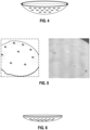
- FIG. 4 is a perspective view schematic of the thermoformed wafer 105 including the microstructures 230 (microlenses), useful within the scope of the present disclosure.
- the thermoformed wafer 105 can be formed with different base curvatures ranging from, for example, 1.00 Diopter to 8.50 Diopter while retaining the structural integrity and optical performance of the microstructures 230.
- FIG. 5 is a schematic and corresponding optical image of a curved thermoformed wafer, useful within the scope of the present disclosure.
- the thermoformed wafers are formed to a low base curve wafer and include 8 or more microlenslets around the film periphery and one microlenslet in the center.
- FIG. 6 is a perspective view schematic of a formed lens with microstructures, useful within the scope of the present disclosure.
- the forming insert 210 base curvature can match the base curve of the formed lens to facilitate lens fabrication, such as a curvature in the range of 1.00 Diopter to 8.50 Diopter and can include several, for example 100 microlenslets, around the film center.
- the plurality of microstructures 205 can be used to mold, for example, refractive micro-structures or diffractive micro/nano-structures.
- the plurality of microstructures 205 can be an inversion of a desired final pattern be formed on the resulting lens after molding.
- the plurality of microstructures 205 can include microlenses or microlenslets or any other type of structure or elements having physical Z deformation/height or depth between 0.1 ⁇ m to 50 ⁇ m and width/length between 0.5 ⁇ m to 2.0 mm. These structures preferably have periodical or pseudo periodical layout but may also have randomized positions.
- microstructures are a grid with constant grid step, honeycomb layout, multiple concentric rings, contiguous e.g., no space in between microstructures.
- These structures may provide optical wave front modification in intensity, curvature, or light deviation, where the intensity of wave front is configured such that structures may be absorptive and may locally absorb wave front intensity with a range from 0% to 100%, where the curvature is configured such that the structure may locally modify wave front curvature with a range of +/- 20 Diopters, and light deviation is configured such that the structure may locally scatter light (refract / diffract) with angle ranging from +/- 1° to +/-30°.
- a distance between structures may range from 0 (contiguous) to 3 times the structure in "X" and/or "Y" size (separate microstructures).
- two optical elements located on a surface of a lens substrate are contiguous if there is a path supported by said surface that links the two optical elements and if along said path one does not reach the basis surface on which the optical elements are located.
- the optical elements are contiguous over a pupil when the optical lens over said pupil comprises no refraction area having a refractive power based on a prescription for said eye of the wearer or a refraction area having a refractive power based on a prescription for said eye of the wearer consisting in a plurality of respectively independent island-shaped areas.
- the two optical elements are contiguous if there is a path linking the two optical elements along part of said path one may not measure the refractive power based on a prescription for the eye of the person.
- optical elements being contiguous can also be defined in a surfacic or surface-oriented manner. A measured surface being between 3 mm 2 and 10 mm 2 is considered. The measured surface comprises a density of "W" optical elements per mm 2 . If in said measured surface, at least 95% of the surface, preferably 98%, has an optical power different from the surface onto which the optical elements are located, said optical elements are considered to be contiguous.
- microstructures which form a microstructured main surface of an ophthalmic lens substrate may include lenslets.
- Lenslets may form bumps and/or cavities (i.e., raised or recessed lenslet structures) at the main surface they are arranged onto.
- the outline of the lenslets may be round or polygonal, for example hexagonal.
- lenslets may be microlenses.
- a microlens may be spherical, toric, cylindrical, prismatic, or aspherical shapes or any combination to make a multi-element shape.
- a microlens may have a single focus point, or cylindrical power, or multi-focal power, non-focusing point, or diffractive. Microlenses can be used to prevent progression of myopia or hyperopia.
- the base lens substrate comprises a base lens providing an optical power for correcting myopia or hyperopia
- the microlenses may provide respectively an optical power greater than the optical power of the base lens if the wearer has myopia, or an optical power lower than the optical power of the base lens if the wearer has hyperopia.
- Lenslets may also be Fresnel type microstructures, diffractive structures such as microlenses defining each a Fresnel structure, permanent technical bumps (raised structures), or phase-shifting elements. It can also be a refractive optical element such as microprisms and a light-diffusing optical element such as small protuberances or cavities, or any type of element generating roughness on the substrate.
- Such lenslets can also be ⁇ -Fresnel lenslets as described in US2021109379 , i.e. Fresnel lenslets which phase function has ⁇ phase jumps at the nominal wavelength, as opposition to unifocal Fresnel lenses which phase jumps are multiple values of 2 ⁇ .
- Such lenslets include structures that have a discontinuous shape.
- the shape of such structures may be described by an altitude function, in terms of distance from the base level of the main surface of the optical lens the lenslet belongs to, which exhibits a discontinuity, or which derivative exhibits a discontinuity.
- the microstructure can be a branding mark, holographic mark, metasurface, or the like.
- Lenslets may have a contour shape being inscribable in a circle having a diameter greater than or equal to 0.5 micrometers ( ⁇ m) and smaller than or equal to 2.0 millimeters (mm). Lenslets may have a height, measured in a direction perpendicular to the main surface they are arranged onto, that is greater than or equal to 0.1 ⁇ m and less than or equal to 50 ⁇ m. Lenslets may have periodical or pseudo periodical layout but may also have randomized positions. One layout for lenslets is a grid with constant grid step, honeycomb layout, multiple concentric rings, contiguous e.g. no space in between microstructures.
- These structures may provide optical wave front modification in intensity, curvature, or light deviation, where the intensity of wave front is configured such that structures may be absorptive and may locally absorb wave front intensity with a range from 0% to 100%, where the curvature is configured such that the structure may locally modify wave front curvature with a range of +/- 10, 20, 500, or 1000 Diopters, and light deviation is configured such that the structure may locally scatter light with angle ranging from +/- 1° to +/- 30°.
- a distance between structures may range from 0 (contiguous) to 3 times the structure (separate microstructures).
- Example 1 - A forming insert has a base curve of 4.50 Diopters and 9 holes capable of pulling vacuum, 8 holes of which are arranged annularly around a central hole.
- a tri-acetyl cellulose film measuring 240 ⁇ m in thickness and 76mm in diameter was heated to 60°C for 8 hours prior to thermoforming.
- the lens wafer was arranged in the forming insert and a vacuum pressure of -0.6 psi was applied to form the lens wafer to the shape of the forming insert.
- the forming insert was heated to a forming temperature of 120°C and the lens wafer was held in place for a residence time of 5 minutes.
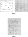
- FIG. 7A is a schematic and corresponding optical image of a curved thermoformed wafer, useful within the scope of the present disclosure.
- FIG. 7A is a schematic and corresponding optical image of a curved thermoformed wafer, useful within the scope of the present disclosure.
- FIG. 7B is the optical image of the curved thermoformed wafer including an overlaid legend, useful within the scope of the present disclosure.
- the general locations of the 8 annular holes around the central hole can be described by positions of hours in a clock.
- the holes were measured using surface profilometry with a Keyence VK-X200 and imaged with a Nikon microscope. The results of the profilometry are described in Table 1. Table 1 - Embossed measurement results.
- FIG. 7C shows a 2D optical microscopy image and a 3D surface profile image at 200X power of the embossed feature at the 12 o'clock position, useful within the scope of the present disclosure.
- FIG. 7D shows a surface microscopy profile at 200X power of the embossed feature at the 12 o'clock position, useful within the scope of the present disclosure.
- the embossed feature at the 12 o'clock position resulted in an embossed depth of 35.9 ⁇ m and an embossed width of 1427.7 ⁇ m.
- FIG. 7E shows a 2D optical microscopy image and a 3D surface profile image at 200X power of the embossed feature at the 1 o'clock position, useful within the scope of the present disclosure.
- FIG. 7F shows a surface microscopy profile at 200X power of the embossed feature at the 1 o'clock position, useful within the scope of the present disclosure.
- the embossed feature at the 1 o'clock position resulted in an embossed depth of 35.97 ⁇ m and an embossed width of 1362.0 ⁇ m.
- FIG. 7G shows a 2D optical microscopy image and a 3D surface profile image at 200X power of the embossed feature at the 3 o'clock position, useful within the scope of the present disclosure.
- FIG. 7H shows a surface microscopy profile at 200X power of the embossed feature at the 3 o'clock position, useful within the scope of the present disclosure.
- the embossed feature at the 3 o'clock position resulted in an embossed depth of 47.37 ⁇ m and an embossed width of 1427.0 ⁇ m.
- FIG. 7I shows a 2D optical microscopy image and a 3D surface profile image at 200X power of the embossed feature at the 4 o'clock position, useful within the scope of the present disclosure.
- FIG. 7J shows a surface microscopy profile at 200X power of the embossed feature at the 4 o'clock position, useful within the scope of the present disclosure.
- the embossed feature at the 4 o'clock position resulted in an embossed depth of 44.1 ⁇ m and an embossed width of 1425.50 ⁇ m.
- FIG. 7K shows a 2D optical microscopy image and a 3D surface profile image at 200X power of the embossed feature at the 6 o'clock position, useful within the scope of the present disclosure.
- FIG. 7L shows a surface microscopy profile at 200X power of the embossed feature at the 6 o'clock position, useful within the scope of the present disclosure.
- the embossed feature at the 6 o'clock position resulted in an embossed depth of 45.45 ⁇ m and an embossed width of 1352.44 ⁇ m.
- FIG. 7M shows a 2D optical microscopy image and a 3D surface profile image at 200X power of the embossed feature at the center position, useful within the scope of the present disclosure.
- FIG. 7N shows a surface microscopy profile at 200X power of the embossed feature at the center position, useful within the scope of the present disclosure.
- the embossed feature at the center position resulted in an embossed depth of 64.12 ⁇ m and an embossed width of 1398.05 ⁇ m.
- the depth values of all 9 microstructures appear to be relatively close to each other, with a small standard deviation.
- the depth of the center microstructure is approximately 20 ⁇ m deeper than the rest of the microstructures.
- the results demonstrate the embossing method (i.e., microforming) for films is possible and promising.
- laminates including thermoplastic optical films or casted optical films are cut into oval shaped wafers.
- the aforementioned wafers are preconditioned at a certain temperature to maintain process uniformity.
- the preconditioned wafers are thermo-mechanically formed to a desired curvature while in parallel imparting microstructure's preferentially onto one side.
- the formed microstructured wafers are subsequently incorporated onto a Finished or Semi-Finished lens by direct front side or back side lamination, or by an injection over-molding process.
- a finished or semifinished lens can be directly inserted onto an optical surface former and the microstructures can be imparted directly onto them, thus eliminating subsequent processing steps.
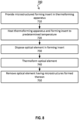
- FIG. 8 is an exemplary flow chart for a method 700 of forming an optical element, useful within the scope of the present disclosure.
- the thermoforming apparatus 200 including the forming insert 210 can be provided.
- the forming insert 210 (and the forming surface 215) can be heated to a predetermined temperature, directly by conductive/convective heating or indirectly by IR radiative heating.
- the optical element (the flat wafer 100) can be disposed in the forming insert 210.
- the optical element can be thermoformed via applying a force to the optical element to contact the forming surface 215.
- the thermoformed optical element including the transferred pattern of microstructures 205 to form the microstructures 230 on the surface of the thermoformed optical element can be removed from the thermoforming apparatus 200.
- Embodiments of the present disclosure may also be as set forth in the following parentheticals.
Landscapes
- Engineering & Computer Science (AREA)
- Mechanical Engineering (AREA)
- Manufacturing & Machinery (AREA)
- Health & Medical Sciences (AREA)
- Ophthalmology & Optometry (AREA)
- Shaping Of Tube Ends By Bending Or Straightening (AREA)
Priority Applications (4)
| Application Number | Priority Date | Filing Date | Title |
|---|---|---|---|
| EP21306818.2A EP4197766A1 (de) | 2021-12-16 | 2021-12-16 | Verfahren zum mikroformen von mikrostrukturierten folien und linsen |
| US18/720,501 US20250050570A1 (en) | 2021-12-16 | 2022-12-13 | Method for microforming microstructured films and lenses |
| CN202280072295.6A CN118176105A (zh) | 2021-12-16 | 2022-12-13 | 微结构膜和透镜的微成形方法 |
| PCT/EP2022/085686 WO2023110916A1 (en) | 2021-12-16 | 2022-12-13 | Method for microforming microstructured films and lenses |
Applications Claiming Priority (1)
| Application Number | Priority Date | Filing Date | Title |
|---|---|---|---|
| EP21306818.2A EP4197766A1 (de) | 2021-12-16 | 2021-12-16 | Verfahren zum mikroformen von mikrostrukturierten folien und linsen |
Publications (1)
| Publication Number | Publication Date |
|---|---|
| EP4197766A1 true EP4197766A1 (de) | 2023-06-21 |
Family
ID=79316932
Family Applications (1)
| Application Number | Title | Priority Date | Filing Date |
|---|---|---|---|
| EP21306818.2A Pending EP4197766A1 (de) | 2021-12-16 | 2021-12-16 | Verfahren zum mikroformen von mikrostrukturierten folien und linsen |
Country Status (4)
| Country | Link |
|---|---|
| US (1) | US20250050570A1 (de) |
| EP (1) | EP4197766A1 (de) |
| CN (1) | CN118176105A (de) |
| WO (1) | WO2023110916A1 (de) |
Citations (4)
| Publication number | Priority date | Publication date | Assignee | Title |
|---|---|---|---|---|
| US20050249919A1 (en) * | 2004-04-29 | 2005-11-10 | Bernd Wolfing | Method and apparatus for forming an optical element and substrate and moulding tool |
| US20210048689A1 (en) * | 2018-03-01 | 2021-02-18 | Essilor International | Lens element |
| US20210354409A1 (en) * | 2018-10-17 | 2021-11-18 | Essilor International | Optical Articles Having Embossed Films Defining Encapsulated Microlenses and Methods of Making the Same |
| US20210356763A1 (en) * | 2018-10-15 | 2021-11-18 | Essilor International | Optical Article Incorporating Optical Elements and Manufacturing Method Thereof |
Family Cites Families (4)
| Publication number | Priority date | Publication date | Assignee | Title |
|---|---|---|---|---|
| US6162376A (en) * | 1999-02-24 | 2000-12-19 | Mead Opthalmics | Compression molding of optical lenses |
| US7777416B2 (en) * | 2007-06-14 | 2010-08-17 | Global Oled Technology Llc | Light emitting device with microlens array |
| US20130344296A1 (en) * | 2012-06-22 | 2013-12-26 | Sabic Innovative Plastics Ip B.V. | Coated film for insert mold decoration, methods for using the same, and articles made thereby |
| EP3546122B1 (de) * | 2018-03-30 | 2020-10-21 | Essilor International | Linsenhalteblock und verfahren zum sperren und entsperren einer optischen linsenkomponente |
-
2021
- 2021-12-16 EP EP21306818.2A patent/EP4197766A1/de active Pending
-
2022
- 2022-12-13 CN CN202280072295.6A patent/CN118176105A/zh active Pending
- 2022-12-13 WO PCT/EP2022/085686 patent/WO2023110916A1/en not_active Ceased
- 2022-12-13 US US18/720,501 patent/US20250050570A1/en active Pending
Patent Citations (5)
| Publication number | Priority date | Publication date | Assignee | Title |
|---|---|---|---|---|
| US20050249919A1 (en) * | 2004-04-29 | 2005-11-10 | Bernd Wolfing | Method and apparatus for forming an optical element and substrate and moulding tool |
| US20210048689A1 (en) * | 2018-03-01 | 2021-02-18 | Essilor International | Lens element |
| US20210109379A1 (en) | 2018-03-01 | 2021-04-15 | Essilor International | Lens element |
| US20210356763A1 (en) * | 2018-10-15 | 2021-11-18 | Essilor International | Optical Article Incorporating Optical Elements and Manufacturing Method Thereof |
| US20210354409A1 (en) * | 2018-10-17 | 2021-11-18 | Essilor International | Optical Articles Having Embossed Films Defining Encapsulated Microlenses and Methods of Making the Same |
Also Published As
| Publication number | Publication date |
|---|---|
| WO2023110916A1 (en) | 2023-06-22 |
| CN118176105A (zh) | 2024-06-11 |
| US20250050570A1 (en) | 2025-02-13 |
Similar Documents
| Publication | Publication Date | Title |
|---|---|---|
| US7861999B2 (en) | Lens molding apparatus | |
| EP4194932A1 (de) | Ophthalmische linse und verfahren zur herstellung einer ophthalmischen linse | |
| CN115413327B (zh) | 用于并入眼科镜片的含光学微结构的层压件 | |
| KR20060047529A (ko) | 광학 소자 형성 방법 및 형성 장치와 기판과 성형 툴 | |
| US9649788B2 (en) | Method of fabricating an array of optical lens elements | |
| CN117642264A (zh) | 用于制作用于注射模制的微结构化嵌件的方法 | |
| CN118159411A (zh) | 用于通过pipc来封装微结构化镜片的方法 | |
| US12572031B2 (en) | Optical microstructure-containing laminate for ophthalmic lens incorporation | |
| CN104626528B (zh) | 一种光学扩散膜片制作方法 | |
| KR20030059200A (ko) | 엠보스 시트의 제조 방법 및 엠보스 시트 | |
| US20250050570A1 (en) | Method for microforming microstructured films and lenses | |
| US20240308161A1 (en) | Composite mold insert for fabricating microstructured lenses | |
| US12508788B2 (en) | Methods, apparatuses, and systems for edge sealing laminate wafers containing a soft deformable inner film | |
| US12521920B2 (en) | Method for generating microstructure on a film by a roller | |
| EP4122689A1 (de) | Metalleinsatz mit geringer wärmeleitfähigkeit mit oberflächenmikrostrukturen | |
| WO2017119398A1 (ja) | 微細構造付き三次元成形体の製造方法 | |
| TWI274898B (en) | A manufacture method of micro-lens |
Legal Events
| Date | Code | Title | Description |
|---|---|---|---|
| PUAI | Public reference made under article 153(3) epc to a published international application that has entered the european phase |
Free format text: ORIGINAL CODE: 0009012 |
|
| STAA | Information on the status of an ep patent application or granted ep patent |
Free format text: STATUS: THE APPLICATION HAS BEEN PUBLISHED |
|
| AK | Designated contracting states |
Kind code of ref document: A1 Designated state(s): AL AT BE BG CH CY CZ DE DK EE ES FI FR GB GR HR HU IE IS IT LI LT LU LV MC MK MT NL NO PL PT RO RS SE SI SK SM TR |
|
| STAA | Information on the status of an ep patent application or granted ep patent |
Free format text: STATUS: REQUEST FOR EXAMINATION WAS MADE |
|
| 17P | Request for examination filed |
Effective date: 20230906 |
|
| RBV | Designated contracting states (corrected) |
Designated state(s): AL AT BE BG CH CY CZ DE DK EE ES FI FR GB GR HR HU IE IS IT LI LT LU LV MC MK MT NL NO PL PT RO RS SE SI SK SM TR |