EP4199031A1 - Optische ladungsteilchenvorrichtung und projektionsverfahren - Google Patents
Optische ladungsteilchenvorrichtung und projektionsverfahren Download PDFInfo
- Publication number
- EP4199031A1 EP4199031A1 EP21215700.2A EP21215700A EP4199031A1 EP 4199031 A1 EP4199031 A1 EP 4199031A1 EP 21215700 A EP21215700 A EP 21215700A EP 4199031 A1 EP4199031 A1 EP 4199031A1
- Authority
- EP
- European Patent Office
- Prior art keywords
- charged
- detector
- sample
- converter
- monitoring
- Prior art date
- Legal status (The legal status is an assumption and is not a legal conclusion. Google has not performed a legal analysis and makes no representation as to the accuracy of the status listed.)
- Withdrawn
Links
- 230000003287 optical effect Effects 0.000 title claims abstract description 200
- 239000002245 particle Substances 0.000 title claims abstract description 175
- 238000000034 method Methods 0.000 title description 53
- 238000012544 monitoring process Methods 0.000 claims abstract description 143
- 238000007689 inspection Methods 0.000 claims abstract description 42
- 230000004044 response Effects 0.000 claims description 20
- 238000005259 measurement Methods 0.000 claims description 8
- 239000000523 sample Substances 0.000 description 171
- 230000004075 alteration Effects 0.000 description 37
- 238000001514 detection method Methods 0.000 description 29
- 238000010586 diagram Methods 0.000 description 26
- 230000008569 process Effects 0.000 description 19
- 239000000758 substrate Substances 0.000 description 16
- 239000000463 material Substances 0.000 description 13
- 238000003491 array Methods 0.000 description 11
- 238000004519 manufacturing process Methods 0.000 description 11
- 230000007547 defect Effects 0.000 description 10
- 238000012545 processing Methods 0.000 description 10
- 238000010894 electron beam technology Methods 0.000 description 9
- 230000000694 effects Effects 0.000 description 8
- 239000013307 optical fiber Substances 0.000 description 8
- 230000000903 blocking effect Effects 0.000 description 7
- 238000003384 imaging method Methods 0.000 description 6
- 239000004065 semiconductor Substances 0.000 description 6
- 239000011248 coating agent Substances 0.000 description 5
- 238000000576 coating method Methods 0.000 description 5
- 230000005855 radiation Effects 0.000 description 5
- 229910052710 silicon Inorganic materials 0.000 description 5
- 239000010703 silicon Substances 0.000 description 5
- 201000009310 astigmatism Diseases 0.000 description 4
- 238000006243 chemical reaction Methods 0.000 description 4
- 238000005286 illumination Methods 0.000 description 4
- 238000012856 packing Methods 0.000 description 4
- 238000007493 shaping process Methods 0.000 description 4
- 238000003860 storage Methods 0.000 description 4
- 235000012431 wafers Nutrition 0.000 description 4
- 230000009286 beneficial effect Effects 0.000 description 3
- 239000000919 ceramic Substances 0.000 description 3
- 230000003750 conditioning effect Effects 0.000 description 3
- 238000012937 correction Methods 0.000 description 3
- 230000001419 dependent effect Effects 0.000 description 3
- 238000013461 design Methods 0.000 description 3
- 239000011521 glass Substances 0.000 description 3
- 239000011810 insulating material Substances 0.000 description 3
- 230000003993 interaction Effects 0.000 description 3
- 229910019655 synthetic inorganic crystalline material Inorganic materials 0.000 description 3
- 238000010276 construction Methods 0.000 description 2
- 238000009826 distribution Methods 0.000 description 2
- 230000005684 electric field Effects 0.000 description 2
- 230000007613 environmental effect Effects 0.000 description 2
- 238000005530 etching Methods 0.000 description 2
- 238000011066 ex-situ storage Methods 0.000 description 2
- 230000002349 favourable effect Effects 0.000 description 2
- 238000012552 review Methods 0.000 description 2
- 238000001228 spectrum Methods 0.000 description 2
- 229910052684 Cerium Inorganic materials 0.000 description 1
- XUIMIQQOPSSXEZ-UHFFFAOYSA-N Silicon Chemical compound [Si] XUIMIQQOPSSXEZ-UHFFFAOYSA-N 0.000 description 1
- 230000009471 action Effects 0.000 description 1
- 238000013459 approach Methods 0.000 description 1
- 230000008901 benefit Effects 0.000 description 1
- 230000005540 biological transmission Effects 0.000 description 1
- 239000003990 capacitor Substances 0.000 description 1
- GWXLDORMOJMVQZ-UHFFFAOYSA-N cerium Chemical compound [Ce] GWXLDORMOJMVQZ-UHFFFAOYSA-N 0.000 description 1
- 229910019990 cerium-doped yttrium aluminum garnet Inorganic materials 0.000 description 1
- 238000004891 communication Methods 0.000 description 1
- 238000004590 computer program Methods 0.000 description 1
- 239000004020 conductor Substances 0.000 description 1
- 239000002178 crystalline material Substances 0.000 description 1
- 238000000151 deposition Methods 0.000 description 1
- 230000008021 deposition Effects 0.000 description 1
- 239000006185 dispersion Substances 0.000 description 1
- 238000006073 displacement reaction Methods 0.000 description 1
- 230000005672 electromagnetic field Effects 0.000 description 1
- 238000001493 electron microscopy Methods 0.000 description 1
- 238000000609 electron-beam lithography Methods 0.000 description 1
- 239000000835 fiber Substances 0.000 description 1
- 239000012467 final product Substances 0.000 description 1
- 238000011065 in-situ storage Methods 0.000 description 1
- 230000010354 integration Effects 0.000 description 1
- 229910052751 metal Inorganic materials 0.000 description 1
- 239000002184 metal Substances 0.000 description 1
- 238000001465 metallisation Methods 0.000 description 1
- 238000012986 modification Methods 0.000 description 1
- 230000004048 modification Effects 0.000 description 1
- 230000005405 multipole Effects 0.000 description 1
- 230000002093 peripheral effect Effects 0.000 description 1
- 238000005498 polishing Methods 0.000 description 1
- 239000000047 product Substances 0.000 description 1
- 230000001902 propagating effect Effects 0.000 description 1
- 230000009467 reduction Effects 0.000 description 1
- 230000035945 sensitivity Effects 0.000 description 1
- 238000000926 separation method Methods 0.000 description 1
- 239000000126 substance Substances 0.000 description 1
- 229910019901 yttrium aluminum garnet Inorganic materials 0.000 description 1
Images






Classifications
-
- H—ELECTRICITY
- H01—ELECTRIC ELEMENTS
- H01J—ELECTRIC DISCHARGE TUBES OR DISCHARGE LAMPS
- H01J37/00—Discharge tubes with provision for introducing objects or material to be exposed to the discharge, e.g. for the purpose of examination or processing thereof
- H01J37/02—Details
- H01J37/22—Optical, image processing or photographic arrangements associated with the tube
- H01J37/224—Luminescent screens or photographic plates for imaging; Apparatus specially adapted therefor, e. g. cameras, TV-cameras, photographic equipment or exposure control; Optical subsystems specially adapted therefor, e. g. microscopes for observing image on luminescent screen
-
- H—ELECTRICITY
- H01—ELECTRIC ELEMENTS
- H01J—ELECTRIC DISCHARGE TUBES OR DISCHARGE LAMPS
- H01J2237/00—Discharge tubes exposing object to beam, e.g. for analysis treatment, etching, imaging
- H01J2237/245—Detection characterised by the variable being measured
- H01J2237/24507—Intensity, dose or other characteristics of particle beams or electromagnetic radiation
- H01J2237/24514—Beam diagnostics including control of the parameter or property diagnosed
Definitions
- a method to project a multibeam of charged particles to a sample comprising:
- the goal of the manufacturing process is to improve the overall yield of the process. For example, to obtain a 75% yield for a 50-step process (where a step can indicate the number of layers formed on a wafer), each individual step must have a yield greater than 99.4%,. If each individual step had a yield of 95%, the overall process yield would be as low as 7%.
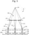
- the condenser lenses 231 may comprise multi-electrode lenses and have a construction based on EP1602121A1 , which document is hereby incorporated by reference in particular to the disclosure of a lens array to split an e-beam into a plurality of sub-beams, with the array providing a lens for each sub-beam.
- the condenser lens array therefore functions as a beam divider, beam splitter, beam generator or beam separator.
- the condenser lens array may take the form of at least two plates, acting as electrodes, with an aperture in each plate aligned with each other and corresponding to the location of a sub-beam. At least two of the plates are maintained during operation at different potentials to achieve the desired lensing effect.
- Each condenser lens in the array directs electrons into a respective sub-beam 211, 212, 213 which is focused at a respective intermediate focus 233.
- the sub-beams diverge with respect to each other.
- the deflectors 235 are positioned in the beamlet paths at, or at least around, the position of the corresponding intermediate focusses 233 or focus points (i.e. points of focus).
- the deflectors are positioned in the beamlet paths at the intermediate image plane of the associated beamlet, i.e. at its focus or focus point.
- the deflectors 235 are configured to operate on the respective beamlets 211, 212, 213.
- Some techniques of aligning the electron optical components include corrector components such as corrector arrays in the electron-optical device, for example as described herein. Such components may operable to achieve improved alignment.
- One such electron optical component is a collimator which may have the functions of aligning and collimating.
- other correctors for example upbeam of a beam limiting aperture array so that the corrector operates on the source beam, present in and associated with the condenser lens (e.g. the condenser lens array) such as proximally downbeam of the condenser lens , the collimator (for example associated with the intermediate focus 233, and the objective lens array.
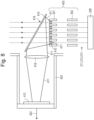
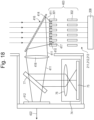
- the light guiding arrangement comprises one or more optical fibers between the mirror 414 and the light sensor 412.
- the optical fibers collect light from the mirror and guide the light to a location further away from the part of the column through which the beams pass, for example away from the path of the beam arrangement.
- Using optical fibers in this way provides further flexibility for positioning of the light sensor 412 (and associated electronics and/or data lines).
- the light sensor 412 can be positioned more remotely from the column.
- the light sensor 412 can be positioned out of the direct line of sight of the mirror 412,
- the converter 410 may comprise an inner annular portion surrounding an aperture and an outer annular portion, radially outwards of the inner annular portion.
- the converter 410 may be divided angularly.
- the scintillator 410 may be provided as sector portions comprising 2, 3, 4, or more portions, for example 8, 12 etc. If the converter 410 is provided as two sectors, each sector portion may be a semi-circle. If the converter 410 is provided as four sectors, each sector portion may be a quadrant. In an example, the converter 410 is divided into quadrants, i.e., four sector portions. Alternatively, the converter 410 may be provided with at least one segment portion.
- the device comprises at least one moveable component.
- the moveable component is configured to move between an operational position and a monitoring position.
- the operation position corresponds to the operational configuration.
- the monitoring position corresponds to the monitoring position.
- the movement is shown by the double ended dashed arrow in FIG. 10 .
- the monitoring detector 64 comprises a monitoring detector element.
- the converter comprises a monitoring detector element for one or more sub-beams of the multi-beam.
- the monitoring detector 64 comprises a plurality of elements for each sub-beam.
- the monitoring detector elements may be comprised in an array, for example a two dimensional array, for example corresponding to the array of sub-beams of the multibeam.
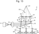
- the mirror 62 and the lens are additional optical components provided so as to aid reading the light signal. That is the mirror 62 and the optical element 63 improve transmission of the light signal from the converter 60 to the optical detector such as the external camera 61. The mirror 62 and the optical element 63 may improve detection and/or collection efficiency.
- the mirror 62 is tilted relative to the converter 60 for example by an optimal angle.
- the mirror may be tilted between 25 and 65 degrees preferably by about 45 degrees. Tilting the mirror 62 helps to direct the light away from the operational beam path. This allows the optical detector such as the external camera 61 to be positioned externally to the operational beam path such as outside of the vacuum.
- the switching deflector 78 comprises a plurality of deflector elements to operate on a path of respective beam paths of the multi-beam.
- the switch deflector 78 comprises a macro deflector is provided configured to operate on all beam paths of the multi-beam.
- the switching deflector array may be omitted.
- the switching deflector array may have a meso switching deflector for which each deflector is operable on a group of sub-beams of the multibeam.
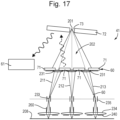
- the mirror 72 is positioned in an upbeam direction of the converter 60. In an embodiment the mirror 72 is between the converter 60 and the source 201. The mirror 72 may be located in a volume that would otherwise be relatively empty. An embodiment of the invention is expected to allow the source beam 202 to be monitored without significantly affecting the mechanical design of parts of the apparatus used during an inspection or metrology process.
- Clause 6 The charged-particle optical apparatus of clause 5, wherein the at least one moveable component comprises a light guiding arrangement configured to guide the light generated by the converter towards the detector.
- Clause 13 The charged-particle apparatus of clause 10 or 12, wherein in the monitoring configuration, the paths of the plurality of beams of the multi-beam are incident on the converter.
- Clause 21 The charged-particle optical apparatus of clause 20, wherein the mirror is positioned in an up-beam direction of the converter, wherein desirably the mirror is between the converter and the source.
- Clause 22 The charged-particle optical apparatus of clause 20 or 21, wherein the mirror comprises an aperture for accommodating the source and/or the source beam.
- a method of projecting a multi-beam of charged particles to a sample comprising: projecting the multi-beam onto locations on the sample, desirably using an objective lens array; receiving signal particles emitted from the sample and generating light in response to the received signal particles, desirably using a plurality of converters, desirably scintillators; guiding the light generated to a light sensing assembly using a light guiding arrangement, wherein the light guiding arrangement comprises a mirror in which is defined a plurality of apertures, allowing passage of the multi-beam through the mirror towards the sample; and splitting the light generated into a plurality of light beams desirably using a beam splitter, preferably for an assessment sensor and a detector; and detecting the generated light, desirably using the assessment sensor and the detector.
Landscapes
- Chemical & Material Sciences (AREA)
- Analytical Chemistry (AREA)
- Analysing Materials By The Use Of Radiation (AREA)
Priority Applications (5)
| Application Number | Priority Date | Filing Date | Title |
|---|---|---|---|
| EP21215700.2A EP4199031A1 (de) | 2021-12-17 | 2021-12-17 | Optische ladungsteilchenvorrichtung und projektionsverfahren |
| PCT/EP2022/082846 WO2023110331A1 (en) | 2021-12-17 | 2022-11-22 | Charged-particle optical apparatus and projection method |
| IL313105A IL313105A (en) | 2021-12-17 | 2022-11-22 | Optical device with charged particles and projection method |
| TW111147692A TW202341213A (zh) | 2021-12-17 | 2022-12-13 | 帶電粒子光學裝置及投影方法 |
| US18/743,011 US20240339294A1 (en) | 2021-12-17 | 2024-06-13 | Charged-particle optical apparatus and projection method |
Applications Claiming Priority (1)
| Application Number | Priority Date | Filing Date | Title |
|---|---|---|---|
| EP21215700.2A EP4199031A1 (de) | 2021-12-17 | 2021-12-17 | Optische ladungsteilchenvorrichtung und projektionsverfahren |
Publications (1)
| Publication Number | Publication Date |
|---|---|
| EP4199031A1 true EP4199031A1 (de) | 2023-06-21 |
Family
ID=78957337
Family Applications (1)
| Application Number | Title | Priority Date | Filing Date |
|---|---|---|---|
| EP21215700.2A Withdrawn EP4199031A1 (de) | 2021-12-17 | 2021-12-17 | Optische ladungsteilchenvorrichtung und projektionsverfahren |
Country Status (1)
| Country | Link |
|---|---|
| EP (1) | EP4199031A1 (de) |
Citations (10)
| Publication number | Priority date | Publication date | Assignee | Title |
|---|---|---|---|---|
| US6538255B1 (en) * | 1999-02-22 | 2003-03-25 | Nikon Corporation | Electron gun and electron-beam optical systems and methods including detecting and adjusting transverse beam-intensity profile, and device manufacturing methods including same |
| EP1602121A2 (de) | 2003-03-10 | 2005-12-07 | Mapper Lithography Ip B.V. | Vorrichtung zur erzeugung einer vielzahl von teilstrahlen |
| US20070057204A1 (en) * | 2005-09-15 | 2007-03-15 | Pieter Kruit | Lithography system, sensor and measuring method |
| US20100276606A1 (en) | 2009-04-29 | 2010-11-04 | Mapper Lithography Ip B.V. | Charged particle optical system comprising an electrostatic deflector |
| WO2012062931A1 (en) * | 2010-11-13 | 2012-05-18 | Mapper Lithography Ip B.V. | Method for determining a distance between two beamlets in a multi-beamlet exposure apparatus |
| WO2013171177A1 (en) * | 2012-05-14 | 2013-11-21 | Mapper Lithography Ip B.V. | Method for determining a beamlet position and method for determining a distance between two beamlets in a multi-beamlet exposure apparatus |
| EP2702595A1 (de) | 2011-04-27 | 2014-03-05 | Mapper Lithography IP B.V. | Geladenes teilchensystem mit einer manipulatorvorrichtung zur manipulation eines oder mehrerer geladener teilchenstrahlen |
| EP2715768A2 (de) | 2011-05-30 | 2014-04-09 | Mapper Lithography IP B.V. | Vorrichtung mit mehreren ladungsträgerteilstrahlen |
| US20190103252A1 (en) * | 2017-09-29 | 2019-04-04 | Nuflare Technology, Inc. | Multi charged particle beam writing apparatus and multi charged particle beam writing method |
| WO2020078660A1 (en) * | 2018-10-19 | 2020-04-23 | Asml Netherlands B.V. | System and method for aligning electron beams in multi-beam inspection apparatus |
-
2021
- 2021-12-17 EP EP21215700.2A patent/EP4199031A1/de not_active Withdrawn
Patent Citations (10)
| Publication number | Priority date | Publication date | Assignee | Title |
|---|---|---|---|---|
| US6538255B1 (en) * | 1999-02-22 | 2003-03-25 | Nikon Corporation | Electron gun and electron-beam optical systems and methods including detecting and adjusting transverse beam-intensity profile, and device manufacturing methods including same |
| EP1602121A2 (de) | 2003-03-10 | 2005-12-07 | Mapper Lithography Ip B.V. | Vorrichtung zur erzeugung einer vielzahl von teilstrahlen |
| US20070057204A1 (en) * | 2005-09-15 | 2007-03-15 | Pieter Kruit | Lithography system, sensor and measuring method |
| US20100276606A1 (en) | 2009-04-29 | 2010-11-04 | Mapper Lithography Ip B.V. | Charged particle optical system comprising an electrostatic deflector |
| WO2012062931A1 (en) * | 2010-11-13 | 2012-05-18 | Mapper Lithography Ip B.V. | Method for determining a distance between two beamlets in a multi-beamlet exposure apparatus |
| EP2702595A1 (de) | 2011-04-27 | 2014-03-05 | Mapper Lithography IP B.V. | Geladenes teilchensystem mit einer manipulatorvorrichtung zur manipulation eines oder mehrerer geladener teilchenstrahlen |
| EP2715768A2 (de) | 2011-05-30 | 2014-04-09 | Mapper Lithography IP B.V. | Vorrichtung mit mehreren ladungsträgerteilstrahlen |
| WO2013171177A1 (en) * | 2012-05-14 | 2013-11-21 | Mapper Lithography Ip B.V. | Method for determining a beamlet position and method for determining a distance between two beamlets in a multi-beamlet exposure apparatus |
| US20190103252A1 (en) * | 2017-09-29 | 2019-04-04 | Nuflare Technology, Inc. | Multi charged particle beam writing apparatus and multi charged particle beam writing method |
| WO2020078660A1 (en) * | 2018-10-19 | 2020-04-23 | Asml Netherlands B.V. | System and method for aligning electron beams in multi-beam inspection apparatus |
Similar Documents
| Publication | Publication Date | Title |
|---|---|---|
| KR102845336B1 (ko) | 하전 입자 다중 빔 칼럼, 하전 입자 다중 빔 칼럼 어레이, 검사 방법 | |
| US12548735B2 (en) | Charged particle assessment tool, inspection method | |
| KR20250144502A (ko) | 검사 장치 | |
| US20230207259A1 (en) | Alignment determination method and computer program | |
| US20240242921A1 (en) | Charged particle apparatus and method | |
| US20240136147A1 (en) | Charged particle-optical device, charged particle apparatus and method | |
| WO2022228943A1 (en) | Charged particle assessment system and method | |
| US20240331968A1 (en) | Charged-particle apparatus, multi-device apparatus, method of using charged-particle apparatus and control method | |
| US20250014855A1 (en) | Charged particle apparatus and method | |
| US20240145208A1 (en) | Charged particle apparatus and method | |
| US20240321547A1 (en) | Charged-particle optical device | |
| US20240339294A1 (en) | Charged-particle optical apparatus and projection method | |
| EP4117014A1 (de) | Ladungsteilchenvorrichtung und -verfahren | |
| CN118414686A (zh) | 带电粒子光学装置和投射方法 | |
| EP4199028A1 (de) | Vorrichtung für geladene teilchen, gerät zur bewertung geladener teilchen, messverfahren und überwachungsverfahren | |
| EP3975222A1 (de) | Beurteilungswerkzeug für geladene partikel, inspektionsverfahren | |
| JP2026076181A (ja) | 電磁シールドを備えた電子光学アセンブリ |
Legal Events
| Date | Code | Title | Description |
|---|---|---|---|
| PUAI | Public reference made under article 153(3) epc to a published international application that has entered the european phase |
Free format text: ORIGINAL CODE: 0009012 |
|
| STAA | Information on the status of an ep patent application or granted ep patent |
Free format text: STATUS: THE APPLICATION HAS BEEN PUBLISHED |
|
| AK | Designated contracting states |
Kind code of ref document: A1 Designated state(s): AL AT BE BG CH CY CZ DE DK EE ES FI FR GB GR HR HU IE IS IT LI LT LU LV MC MK MT NL NO PL PT RO RS SE SI SK SM TR |
|
| STAA | Information on the status of an ep patent application or granted ep patent |
Free format text: STATUS: THE APPLICATION IS DEEMED TO BE WITHDRAWN |
|
| 18D | Application deemed to be withdrawn |
Effective date: 20231222 |