EP4199052B1 - Schéma de métallisation pour un circuit intégré - Google Patents
Schéma de métallisation pour un circuit intégré Download PDFInfo
- Publication number
- EP4199052B1 EP4199052B1 EP21215780.4A EP21215780A EP4199052B1 EP 4199052 B1 EP4199052 B1 EP 4199052B1 EP 21215780 A EP21215780 A EP 21215780A EP 4199052 B1 EP4199052 B1 EP 4199052B1
- Authority
- EP
- European Patent Office
- Prior art keywords
- electrically conductive
- lines
- conductive line
- mob
- forming
- Prior art date
- Legal status (The legal status is an assumption and is not a legal conclusion. Google has not performed a legal analysis and makes no representation as to the accuracy of the status listed.)
- Active
Links
Images





Classifications
-
- H—ELECTRICITY
- H10—SEMICONDUCTOR DEVICES; ELECTRIC SOLID-STATE DEVICES NOT OTHERWISE PROVIDED FOR
- H10W—GENERIC PACKAGES, INTERCONNECTIONS, CONNECTORS OR OTHER CONSTRUCTIONAL DETAILS OF DEVICES COVERED BY CLASS H10
- H10W20/00—Interconnections in chips, wafers or substrates
- H10W20/01—Manufacture or treatment
- H10W20/031—Manufacture or treatment of conductive parts of the interconnections
- H10W20/069—Manufacture or treatment of conductive parts of the interconnections by forming self-aligned vias or self-aligned contact plugs
-
- H—ELECTRICITY
- H10—SEMICONDUCTOR DEVICES; ELECTRIC SOLID-STATE DEVICES NOT OTHERWISE PROVIDED FOR
- H10D—INORGANIC ELECTRIC SEMICONDUCTOR DEVICES
- H10D62/00—Semiconductor bodies, or regions thereof, of devices having potential barriers
- H10D62/10—Shapes, relative sizes or dispositions of the regions of the semiconductor bodies; Shapes of the semiconductor bodies
- H10D62/117—Shapes of semiconductor bodies
- H10D62/118—Nanostructure semiconductor bodies
- H10D62/119—Nanowire, nanosheet or nanotube semiconductor bodies
- H10D62/121—Nanowire, nanosheet or nanotube semiconductor bodies oriented parallel to substrates
-
- H—ELECTRICITY
- H10—SEMICONDUCTOR DEVICES; ELECTRIC SOLID-STATE DEVICES NOT OTHERWISE PROVIDED FOR
- H10D—INORGANIC ELECTRIC SEMICONDUCTOR DEVICES
- H10D62/00—Semiconductor bodies, or regions thereof, of devices having potential barriers
- H10D62/10—Shapes, relative sizes or dispositions of the regions of the semiconductor bodies; Shapes of the semiconductor bodies
- H10D62/117—Shapes of semiconductor bodies
- H10D62/118—Nanostructure semiconductor bodies
- H10D62/119—Nanowire, nanosheet or nanotube semiconductor bodies
- H10D62/122—Nanowire, nanosheet or nanotube semiconductor bodies oriented at angles to substrates, e.g. perpendicular to substrates
-
- H—ELECTRICITY
- H10—SEMICONDUCTOR DEVICES; ELECTRIC SOLID-STATE DEVICES NOT OTHERWISE PROVIDED FOR
- H10D—INORGANIC ELECTRIC SEMICONDUCTOR DEVICES
- H10D84/00—Integrated devices formed in or on semiconductor substrates that comprise only semiconducting layers, e.g. on Si wafers or on GaAs-on-Si wafers
- H10D84/01—Manufacture or treatment
- H10D84/0123—Integrating together multiple components covered by H10D12/00 or H10D30/00, e.g. integrating multiple IGBTs
- H10D84/0126—Integrating together multiple components covered by H10D12/00 or H10D30/00, e.g. integrating multiple IGBTs the components including insulated gates, e.g. IGFETs
- H10D84/0165—Integrating together multiple components covered by H10D12/00 or H10D30/00, e.g. integrating multiple IGBTs the components including insulated gates, e.g. IGFETs the components including complementary IGFETs, e.g. CMOS devices
- H10D84/0186—Manufacturing their interconnections or electrodes, e.g. source or drain electrodes
-
- H—ELECTRICITY
- H10—SEMICONDUCTOR DEVICES; ELECTRIC SOLID-STATE DEVICES NOT OTHERWISE PROVIDED FOR
- H10D—INORGANIC ELECTRIC SEMICONDUCTOR DEVICES
- H10D84/00—Integrated devices formed in or on semiconductor substrates that comprise only semiconducting layers, e.g. on Si wafers or on GaAs-on-Si wafers
- H10D84/01—Manufacture or treatment
- H10D84/0123—Integrating together multiple components covered by H10D12/00 or H10D30/00, e.g. integrating multiple IGBTs
- H10D84/0126—Integrating together multiple components covered by H10D12/00 or H10D30/00, e.g. integrating multiple IGBTs the components including insulated gates, e.g. IGFETs
- H10D84/0165—Integrating together multiple components covered by H10D12/00 or H10D30/00, e.g. integrating multiple IGBTs the components including insulated gates, e.g. IGFETs the components including complementary IGFETs, e.g. CMOS devices
- H10D84/0188—Manufacturing their isolation regions
-
- H—ELECTRICITY
- H10—SEMICONDUCTOR DEVICES; ELECTRIC SOLID-STATE DEVICES NOT OTHERWISE PROVIDED FOR
- H10D—INORGANIC ELECTRIC SEMICONDUCTOR DEVICES
- H10D84/00—Integrated devices formed in or on semiconductor substrates that comprise only semiconducting layers, e.g. on Si wafers or on GaAs-on-Si wafers
- H10D84/01—Manufacture or treatment
- H10D84/0123—Integrating together multiple components covered by H10D12/00 or H10D30/00, e.g. integrating multiple IGBTs
- H10D84/0126—Integrating together multiple components covered by H10D12/00 or H10D30/00, e.g. integrating multiple IGBTs the components including insulated gates, e.g. IGFETs
- H10D84/0165—Integrating together multiple components covered by H10D12/00 or H10D30/00, e.g. integrating multiple IGBTs the components including insulated gates, e.g. IGFETs the components including complementary IGFETs, e.g. CMOS devices
- H10D84/0193—Integrating together multiple components covered by H10D12/00 or H10D30/00, e.g. integrating multiple IGBTs the components including insulated gates, e.g. IGFETs the components including complementary IGFETs, e.g. CMOS devices the components including FinFETs
-
- H—ELECTRICITY
- H10—SEMICONDUCTOR DEVICES; ELECTRIC SOLID-STATE DEVICES NOT OTHERWISE PROVIDED FOR
- H10D—INORGANIC ELECTRIC SEMICONDUCTOR DEVICES
- H10D84/00—Integrated devices formed in or on semiconductor substrates that comprise only semiconducting layers, e.g. on Si wafers or on GaAs-on-Si wafers
- H10D84/01—Manufacture or treatment
- H10D84/02—Manufacture or treatment characterised by using material-based technologies
- H10D84/03—Manufacture or treatment characterised by using material-based technologies using Group IV technology, e.g. silicon technology or silicon-carbide [SiC] technology
- H10D84/038—Manufacture or treatment characterised by using material-based technologies using Group IV technology, e.g. silicon technology or silicon-carbide [SiC] technology using silicon technology, e.g. SiGe
-
- H—ELECTRICITY
- H10—SEMICONDUCTOR DEVICES; ELECTRIC SOLID-STATE DEVICES NOT OTHERWISE PROVIDED FOR
- H10D—INORGANIC ELECTRIC SEMICONDUCTOR DEVICES
- H10D84/00—Integrated devices formed in or on semiconductor substrates that comprise only semiconducting layers, e.g. on Si wafers or on GaAs-on-Si wafers
- H10D84/80—Integrated devices formed in or on semiconductor substrates that comprise only semiconducting layers, e.g. on Si wafers or on GaAs-on-Si wafers characterised by the integration of at least one component covered by groups H10D12/00 or H10D30/00, e.g. integration of IGFETs
- H10D84/82—Integrated devices formed in or on semiconductor substrates that comprise only semiconducting layers, e.g. on Si wafers or on GaAs-on-Si wafers characterised by the integration of at least one component covered by groups H10D12/00 or H10D30/00, e.g. integration of IGFETs of only field-effect components
- H10D84/83—Integrated devices formed in or on semiconductor substrates that comprise only semiconducting layers, e.g. on Si wafers or on GaAs-on-Si wafers characterised by the integration of at least one component covered by groups H10D12/00 or H10D30/00, e.g. integration of IGFETs of only field-effect components of only insulated-gate FETs [IGFET]
- H10D84/85—Complementary IGFETs, e.g. CMOS
- H10D84/853—Complementary IGFETs, e.g. CMOS comprising FinFETs
-
- H—ELECTRICITY
- H10—SEMICONDUCTOR DEVICES; ELECTRIC SOLID-STATE DEVICES NOT OTHERWISE PROVIDED FOR
- H10P—GENERIC PROCESSES OR APPARATUS FOR THE MANUFACTURE OR TREATMENT OF DEVICES COVERED BY CLASS H10
- H10P50/00—Etching of wafers, substrates or parts of devices
- H10P50/71—Etching of wafers, substrates or parts of devices using masks for conductive or resistive materials
-
- H—ELECTRICITY
- H10—SEMICONDUCTOR DEVICES; ELECTRIC SOLID-STATE DEVICES NOT OTHERWISE PROVIDED FOR
- H10W—GENERIC PACKAGES, INTERCONNECTIONS, CONNECTORS OR OTHER CONSTRUCTIONAL DETAILS OF DEVICES COVERED BY CLASS H10
- H10W20/00—Interconnections in chips, wafers or substrates
- H10W20/01—Manufacture or treatment
- H10W20/031—Manufacture or treatment of conductive parts of the interconnections
- H10W20/063—Manufacture or treatment of conductive parts of the interconnections by forming conductive members before forming protective insulating material
-
- H—ELECTRICITY
- H10—SEMICONDUCTOR DEVICES; ELECTRIC SOLID-STATE DEVICES NOT OTHERWISE PROVIDED FOR
- H10W—GENERIC PACKAGES, INTERCONNECTIONS, CONNECTORS OR OTHER CONSTRUCTIONAL DETAILS OF DEVICES COVERED BY CLASS H10
- H10W20/00—Interconnections in chips, wafers or substrates
- H10W20/01—Manufacture or treatment
- H10W20/031—Manufacture or treatment of conductive parts of the interconnections
- H10W20/063—Manufacture or treatment of conductive parts of the interconnections by forming conductive members before forming protective insulating material
- H10W20/0633—Manufacture or treatment of conductive parts of the interconnections by forming conductive members before forming protective insulating material using subtractive patterning of the conductive members
-
- H—ELECTRICITY
- H10—SEMICONDUCTOR DEVICES; ELECTRIC SOLID-STATE DEVICES NOT OTHERWISE PROVIDED FOR
- H10W—GENERIC PACKAGES, INTERCONNECTIONS, CONNECTORS OR OTHER CONSTRUCTIONAL DETAILS OF DEVICES COVERED BY CLASS H10
- H10W20/00—Interconnections in chips, wafers or substrates
- H10W20/01—Manufacture or treatment
- H10W20/031—Manufacture or treatment of conductive parts of the interconnections
- H10W20/069—Manufacture or treatment of conductive parts of the interconnections by forming self-aligned vias or self-aligned contact plugs
- H10W20/0693—Manufacture or treatment of conductive parts of the interconnections by forming self-aligned vias or self-aligned contact plugs by forming self-aligned vias
-
- H—ELECTRICITY
- H10—SEMICONDUCTOR DEVICES; ELECTRIC SOLID-STATE DEVICES NOT OTHERWISE PROVIDED FOR
- H10W—GENERIC PACKAGES, INTERCONNECTIONS, CONNECTORS OR OTHER CONSTRUCTIONAL DETAILS OF DEVICES COVERED BY CLASS H10
- H10W20/00—Interconnections in chips, wafers or substrates
- H10W20/01—Manufacture or treatment
- H10W20/031—Manufacture or treatment of conductive parts of the interconnections
- H10W20/0698—Local interconnections
-
- H—ELECTRICITY
- H10—SEMICONDUCTOR DEVICES; ELECTRIC SOLID-STATE DEVICES NOT OTHERWISE PROVIDED FOR
- H10W—GENERIC PACKAGES, INTERCONNECTIONS, CONNECTORS OR OTHER CONSTRUCTIONAL DETAILS OF DEVICES COVERED BY CLASS H10
- H10W20/00—Interconnections in chips, wafers or substrates
- H10W20/40—Interconnections external to wafers or substrates, e.g. back-end-of-line [BEOL] metallisations or vias connecting to gate electrodes
- H10W20/41—Interconnections external to wafers or substrates, e.g. back-end-of-line [BEOL] metallisations or vias connecting to gate electrodes characterised by their conductive parts
- H10W20/42—Vias, e.g. via plugs
-
- B—PERFORMING OPERATIONS; TRANSPORTING
- B82—NANOTECHNOLOGY
- B82Y—SPECIFIC USES OR APPLICATIONS OF NANOSTRUCTURES; MEASUREMENT OR ANALYSIS OF NANOSTRUCTURES; MANUFACTURE OR TREATMENT OF NANOSTRUCTURES
- B82Y10/00—Nanotechnology for information processing, storage or transmission, e.g. quantum computing or single electron logic
-
- H—ELECTRICITY
- H10—SEMICONDUCTOR DEVICES; ELECTRIC SOLID-STATE DEVICES NOT OTHERWISE PROVIDED FOR
- H10D—INORGANIC ELECTRIC SEMICONDUCTOR DEVICES
- H10D30/00—Field-effect transistors [FET]
- H10D30/40—FETs having zero-dimensional [0D], one-dimensional [1D] or two-dimensional [2D] charge carrier gas channels
- H10D30/43—FETs having zero-dimensional [0D], one-dimensional [1D] or two-dimensional [2D] charge carrier gas channels having one-dimensional [1D] charge carrier gas channels, e.g. quantum wire FETs or transistors having 1D quantum-confined channels
-
- H—ELECTRICITY
- H10—SEMICONDUCTOR DEVICES; ELECTRIC SOLID-STATE DEVICES NOT OTHERWISE PROVIDED FOR
- H10D—INORGANIC ELECTRIC SEMICONDUCTOR DEVICES
- H10D84/00—Integrated devices formed in or on semiconductor substrates that comprise only semiconducting layers, e.g. on Si wafers or on GaAs-on-Si wafers
- H10D84/80—Integrated devices formed in or on semiconductor substrates that comprise only semiconducting layers, e.g. on Si wafers or on GaAs-on-Si wafers characterised by the integration of at least one component covered by groups H10D12/00 or H10D30/00, e.g. integration of IGFETs
- H10D84/82—Integrated devices formed in or on semiconductor substrates that comprise only semiconducting layers, e.g. on Si wafers or on GaAs-on-Si wafers characterised by the integration of at least one component covered by groups H10D12/00 or H10D30/00, e.g. integration of IGFETs of only field-effect components
- H10D84/83—Integrated devices formed in or on semiconductor substrates that comprise only semiconducting layers, e.g. on Si wafers or on GaAs-on-Si wafers characterised by the integration of at least one component covered by groups H10D12/00 or H10D30/00, e.g. integration of IGFETs of only field-effect components of only insulated-gate FETs [IGFET]
- H10D84/85—Complementary IGFETs, e.g. CMOS
-
- H—ELECTRICITY
- H10—SEMICONDUCTOR DEVICES; ELECTRIC SOLID-STATE DEVICES NOT OTHERWISE PROVIDED FOR
- H10P—GENERIC PROCESSES OR APPARATUS FOR THE MANUFACTURE OR TREATMENT OF DEVICES COVERED BY CLASS H10
- H10P50/00—Etching of wafers, substrates or parts of devices
- H10P50/20—Dry etching; Plasma etching; Reactive-ion etching
- H10P50/26—Dry etching; Plasma etching; Reactive-ion etching of conductive or resistive materials
- H10P50/264—Dry etching; Plasma etching; Reactive-ion etching of conductive or resistive materials by chemical means
- H10P50/266—Dry etching; Plasma etching; Reactive-ion etching of conductive or resistive materials by chemical means by vapour etching only
- H10P50/267—Dry etching; Plasma etching; Reactive-ion etching of conductive or resistive materials by chemical means by vapour etching only using plasmas
-
- H—ELECTRICITY
- H10—SEMICONDUCTOR DEVICES; ELECTRIC SOLID-STATE DEVICES NOT OTHERWISE PROVIDED FOR
- H10W—GENERIC PACKAGES, INTERCONNECTIONS, CONNECTORS OR OTHER CONSTRUCTIONAL DETAILS OF DEVICES COVERED BY CLASS H10
- H10W20/00—Interconnections in chips, wafers or substrates
- H10W20/40—Interconnections external to wafers or substrates, e.g. back-end-of-line [BEOL] metallisations or vias connecting to gate electrodes
- H10W20/41—Interconnections external to wafers or substrates, e.g. back-end-of-line [BEOL] metallisations or vias connecting to gate electrodes characterised by their conductive parts
- H10W20/44—Conductive materials thereof
- H10W20/4403—Conductive materials thereof based on metals, e.g. alloys, metal silicides
- H10W20/4437—Conductive materials thereof based on metals, e.g. alloys, metal silicides the principal metal being a transition metal
- H10W20/4441—Conductive materials thereof based on metals, e.g. alloys, metal silicides the principal metal being a transition metal the principal metal being a refractory metal
Definitions
- the present invention relates to the field of integrated circuits, and more in particular to a metallization scheme for forming an integrated circuit.
- reducing the cell height also reduces the number of metal track lines per standard cell. This has an impact on how one can connect one circuit to another circuit on the wafer. Indeed, reducing the number of metal track lines per standard cell also reduces the routability of the lower metal layers of the standard cell due to high pin density, low pin accessibility, and limited routing resources.
- the cell height remains stuck at the "five-track” level, i.e., a cell height that can vertically accommodate five tracks to access the pins.
- US2021/143085 A1 , EP3913659 A1 and US2021/296231 A1 disclose prior art methods of forming self-aligned top via structures over metal lines.
- the present invention relates to a method for forming an integrated circuit or an intermediate in the formation thereof comprising the steps of:
- Fig. 1 shows two examples of standard cells of the prior art having each metal track extending horizontally along the vertical axis of the cell.
- the horizontal and vertical axes are defined with respect to the cell observed from above the substrate and oriented so that the transistor channel is oriented horizontally.
- Such cells can be referred to as HVH cells because the first level of conductive lines has its lines extending horizontally (H), and since each successive level alternates in orientation.
- the first level of conductive lines has its lines extending vertically (V).
- VHV cells Such cells can, therefore, be referred to as VHV cells.
- Coupled should not be interpreted as being restricted to direct connections only.
- the terms “coupled” and “connected”, along with their derivatives, may be used. It should be understood that these terms are not intended as synonyms for each other.
- the scope of the expression “a device A coupled to a device B” should not be limited to devices or systems wherein an output of device A is directly connected to an input of device B. It means that there exists a path between an output of A and an input of B which may be a path including other devices or means.
- Coupled may mean that two or more elements are either in direct physical or electrical contact, or that two or more elements are not in direct contact with each other but yet still co-operate or interact with each other.
- an element described herein of an apparatus embodiment is an example of a means for carrying out the function performed by the element for the purpose of carrying out the invention.
- the present invention relates to a method for forming an integrated circuit or an intermediate in the formation thereof comprising the steps of:
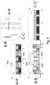
- Step g assures that the third and fourth electrically conductive vias (Vint1 , and Vint2) are self-aligned with the first and second electrically conductive lines (Mintla, Mintlb). Even if there would be variability in the width or position of the first and second electrically conductive lines (Mintla, Mintlb), step g ensures that the third and fourth electrically conductive vias (Vint1, Vint2) are perfectly aligned with the first and second electrically conductive lines (Mintla, Mintlb) respectively. This is a self-correcting mechanism. These vias going down from the set of second electrically conductive lines (Mintl) have for purpose carrying signals that have to reach the source and the drain. Connecting the electrically conductive lines (Mintl) with the source or drain contact (M0A) requires an electrical connection. The method according to the first aspect provides this connection.
- the method may further comprise the steps of:
- the hard mask lines (14l) are typically used twice as a mask, first for forming the electrically conductive vias (Vint1, and Vint2) aligned with the electrically conductive lines (Mintl), and second for forming said interruption (17) aligned with the first gap (15) between the third and the fourth electrically conductive via (Vint1, Vint2).
- step g ensures that the third and fourth electrically conductive vias (Vint1 , Vint2) are perfectly aligned with the first and second electrically conductive lines (Mintla, Mintlb) respectively and that the interruption is perfectly aligned with the first gap. This is a self-correcting mechanism.
- the electrically conductive material making the second electrically conductive lines (Mintl) is different from the electrically conductive material making the first electrically conductive line (MOB) and can be etched selectively with respect to the first electrically conductive line (MOB) during step i. That way, even if the hard mask lines (14l) are entirely consumed before or during step i, step i can still occur. However, the penalty of losing the hard mask lines (14l) is that the possibility to process the vias (V1) self-aligned to the second electrically conductive lines (Mintl) in step j (see below) is lost. It is therefore preferred if the hard mask lines (14l) are not entirely consumed before the end of step i.
- the method may further comprise, typically after step i, the step j of forming:
- step j may comprise:
- step ii the hard mask (14) is removed selectively with respect to the dielectric material (18), and most typically with respect to the dielectric material (18) and any material exposed during step ii which is not the hard mask (14).
- the first electrically conductive via (V0A1) is electrically connecting the first electrically conductive line (MOB) with a first electrically conductive contact (MOA1) on a first side, here the p-type side (5p), of a first (3a) of the transistor structures (3a, 3b), while the second electrically conductive via (V0A2) is electrically connecting the first electrically conductive line (MOB) with a second electrically conductive contact (M0A2) on a first side, here also a p-type side (5p), of a second (3b) of the transistor structures (3b).
- first electrically conductive via (V0A1) is electrically connecting the first electrically conductive line (MOB) with a first electrically conductive contact (M0A1) on a first side, here the n-type side (5n), of a first (3a) of the transistor structures (3a, 3b), while the second electrically conductive via (V0A2) is electrically connecting the first electrically conductive line (MOB) with a second electrically conductive contact (M0A2) on a first side, here also an n-type side (5p), of a second (3b) of the transistor structures (3a, 3b).
- FIG. 3 Yet another alternative starting point for the method of the first aspect is depicted in Fig. 3 where the first electrically conductive via (V0A1) is electrically connecting the first electrically conductive line (MOB) with a first electrically conductive contact (MOA1) on a first side, here the p-type side (5p), of a first (3a) of the transistor structures (3a, 3b), while the second electrically conductive via (V0A2) is electrically connecting the first electrically conductive line (MOB) with a second electrically conductive contact (M0A2) on a first side, here an n-type side (5n), of a second (3b) of the transistor structures (3a, 3b).
- V0A1 is electrically connecting the first electrically conductive line (MOB) with a first electrically conductive contact (MOA1) on a first side, here the p-type side (5p), of a first (3a) of the transistor structures (3a, 3b)
- V0A2 is electrically connecting the first electrically
- first electrically conductive via (V0A1) is electrically connecting the first electrically conductive line (MOB) with a first electrically conductive contact (M0A1) on a first side, here the n-type side (5n), of a first (3a) of the transistor structures (3a, 3b), while the second electrically conductive via (V0A2) is electrically connecting the first electrically conductive line (MOB) with a second electrically conductive contact (M0A2) on a first side, here a p-type side (5p), of a second (3b) of the transistor structures (3a, 3b).
- the method of the first aspect may be for forming a standard cell of the integrated circuit or of the intermediate in the formation thereof.
- the standard cell may comprise four second electrically conductive lines (Mintl) and more than four third electrically conductive lines (M1l).
- the two transistor structures (3a, 3b) may be two nanosheet transistor structures (3a, 3b), each nanosheet transistor structure comprising two nanosheet stacks, one stack forming the pMOS side (5p) of a first doping type, and another stack forming the nMOS side (5n) of a second doping type, each side (5p, 5n) comprising a plurality of vertically stacked nanosheets (7), said plurality forming a channel structure, a source portion, and a drain portion, the source portion and the drain portion being horizontally separated by said channel structure.
- the two transistor structures (3a, 3b) may be two transistor structures (3a, 3b), wherein the pMOS side (5p) of a first doping type and the nMOS side (5n) of a second doping type are separated by a dielectric wall (6), each side (5p, 5n) comprising a plurality of vertically stacked nanosheets (7), said plurality forming a channel structure, a source portion, and a drain portion, the source portion and the drain portion being horizontally separated by said channel structure, each nanosheet (7) having one side (8) touching said dielectric wall (6).
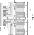
- Such transistor structures are called forksheet transistor structures and a cross-section therethrough is depicted in Fig. 12 .
- the dielectric separation may be made of SiO 2 .
- the gate may comprise a gate metal (5) such as W.
- a gate plug (19) is typically present above the gate metal (5).
- Si 3 N 4 can be used.
- Gate spacers (3) on both sides of the gate are typically present. These spacers (3) can for instance be made of S 3 N 4 or silicon oxicarbide.
- An example of gate structure (9) is visible in Fig. 3 .
- the source and the drain electrically conductive contacts can for instance be SiGe:B (p-MOS) or Si:P (n-MOS).
- the first electrically conductive line (MOB) may be embedded in a dielectric material (8).
- the first electrically conductive line is provided as part of a set of parallel first electrically conductive lines (MOB), all arranged within a first metallization level and each extending along a same first direction.
- the set of first electrically conductive lines (MOB) may be arranged at a pitch of from 20 to 60 nm, preferably, from 30 to 50 nm, more preferably from 35 to 45 nm, yet more preferably from 37 to 41 nm, and most preferably from 38 to 40 nm.
- This pitch being relatively large, there is enough space between the set of first electrically conductive lines (MOB) to form a via connecting directly a line amongst the set of second electrically conductive lines (Mintl) with a gate.
- the formation of this connection does not form part of the present application.
- the planar dielectric material may for instance be SiO 2 .
- the opening performed during step c may be obtained by plasma etching through a hard mask.
- each of the first electrically conductive line (MOB), the first and second electrically conductive vias (VOA1, V0A2), the planar electrically conductive material (13), and the set of second electrically conductive lines (Mintl), may be made of a metal independently selected from metals such as Cu, Mo, Ru, or W, amongst others.
- the set of parallel lines (14l) may be equidistant.
- the set of parallel lines (14l) may be arranged at a pitch of from 9 to 30 nm, preferably, from 12 to 25 nm, more preferably from 14 to 22 nm, yet more preferably from 16 to 20 nm, and most preferably from 18 to 20 nm.
- Step g of etching the electrically conductive layer (Mint) and the planar electrically conductive material may be performed by any suitable method. For instance, if the electrically conductive layer (Mint) and the planar electrically conductive material (13) are both made of Ru, etching can be performed by plasma etching using Cl 2 and/or O 2 and Cl 2 as etchant gas in an inductively coupled plasma etching chamber.
- the first electrically conductive line (MOB) can be made of either the same conductive material as a top portion of the planar electrically conductive material (13) or another conductive material as a top portion of the planar electrically conductive material (13).
- step d comprises filling the opening (11) with a planar electrically conductive material (13) comprising a bottom portion made of a different conductive material than a top portion, wherein the conductive material making the bottom portion is different from the conductive material making the first electrically conductive line (MOB) and can be etched selectively with respect to the first electrically conductive line (MOB) during step g.
- the thickness of the bottom portion is preferably smaller than the thickness of the top portion.
- the bottom portion serves as an etch stop layer.
- step d comprises filling the opening (11) with a single planar electrically conductive material (13) which is different from the conductive material making the first electrically conductive line (MOB) and which can be etched selectively with respect to the first electrically conductive line (MOB) during step g.
- the set of second electrically conductive lines may be arranged at a pitch of from 9 to 30 nm, preferably, from 12 to 25 nm, more preferably from 14 to 22 nm, yet more preferably from 16 to 20 nm, and most preferably from 18 to 20 nm.
- the pitch of the set of parallel lines (14l) is the same as the pitch of the set of second electrically conductive lines (Mintl).
- the set of second electrically conductive lines (Mintl) may be arranged at a pitch and the width of the interruption (17) is equal to 0.5 times the pitch.
- the distance separating the third electrically conductive via (Vint1) and the fourth electrically conductive via (Vint2) is 0.5 times the pitch of the set of second electrically conductive lines (Mintl).
- the width of each of the third and fourth vias (Vint1, Vint2) measured along the first direction is preferably from 5 to 13 nm, more preferably from 6 to 12 nm, yet more preferably from 7 to 11 nm, and most preferably from 8 to 10 nm. Typically, the width for these two vias is 9 nm.
- the distance separating the third electrically conductive via (Vint1) and the fourth electrically conductive via (Vint2) is preferably from 5 to 13 nm, more preferably from 6 to 12 nm, yet more preferably from 7 to 11 nm, and most preferably from 8 to 10 nm. Typically, these two vias are separated by 9 nm.
- the hard mask (14) is preferably sufficiently resistant to the etching so that by the time step i is finished, some hard mask material remains. This way, the set of second electrically conductive lines (Mintl) is not consumed during step i.
- the interruption (17) formed in step i may be from 5 to 13 nm, more preferably from 6 to 12 nm, yet more preferably from 7 to 11 nm, and most preferably from 8 to 10 nm. Typically, this interruption has a width of 9 nm. Such a small interruption, let alone with perfect alignment to the gap, has up to now been very challenging. It is, however, easily achieved with the method of the present invention.
Landscapes
- Internal Circuitry In Semiconductor Integrated Circuit Devices (AREA)
- Design And Manufacture Of Integrated Circuits (AREA)
Claims (14)
- Un procédé de formation d'un circuit intégré ou d'un intermédiaire dans la formation de celui-ci comprenant les étapes de :a. Fournir une structure semi-conductrice (2) comprenanti. deux structures de transistor (3a, 3b) séparées par une séparation diélectrique (4), chaque structure de transistor (3a, 3b) comprenant un côté pMOS (5p) d'un premier type de dopage et un côté nMOS (5n) d'un second type de dopage, chaque côté formant une structure de canal, une portion de source et une portion de drain, la portion de source et la portion de drain étant séparées horizontalement par ladite structure de canal,ii. une structure de grille (9) sur la structure de canal,iii. des contacts électriquement conducteurs (M0A1, M0A2) couplés électriquement à la portion de source et à la portion de drain de chaque côté (5p, 5n) de chaque structure de transistor (3a, 3b),iv. une première ligne électriquement conductrice (MOB) disposée dans un premier niveau de métallisation et s'étendant le long d'une première direction, la première ligne électriquement conductrice (MOB) s'étendant au-dessus d'au moins une partie de chaque structure de transistor (3a, 3b),v. un premier via électriquement conducteur (V0A1) connectant électriquement la première ligne électriquement conductrice (MOB) à un premier contact électriquement conducteur (M0A1) sur un premier côté (5n, 5p) d'une première (3a) des structures de transistor (3a, 3b),vi. un second via électriquement conducteur (V0A2) connectant électriquement la première ligne électriquement conductrice (MOB) à un second contact électriquement conducteur (M0A2) sur un premier côté (5n, 5p) d'une seconde (3b) des structures de transistor (3a, 3b),b. fournir un matériau diélectrique plan (10) en contact physique avec une surface supérieure de la première ligne électriquement conductrice (MOB),c. former une ouverture (11) dans le matériau diélectrique plan (10), ladite ouverture (11) exposant une partie (12) de la première ligne électriquement conductrice (MOB), ladite partie (12) ayant une longueur (L) supérieure à une longueur (1) de la séparation diélectrique (4) lorsque les deux longueurs sont mesurées dans la première direction, dans lequel la longueur (L) de la partie (12) comprend la longueur (1) de la séparation diélectrique (4) lorsque la dernière (1) est projetée verticalement sur la longueur (L) de ladite partie (12),d. remplir l'ouverture (11) avec un matériau électriquement conducteur plan (13),e. former une couche électriquement conductrice (Mint) disposée dans un second niveau de métallisation, la couche électriquement conductrice (Mint) étant en contact physique avec le matériau diélectrique plan (10) et en contact physique et électrique avec le matériau électriquement conducteur (13),f. Fournir un masque dur (14) comprenant un ensemble de lignes parallèles (141) en contact physique avec une surface supérieure de la couche électriquement conductrice (Mint) et s'étendant le long d'une seconde direction, perpendiculaire à la première direction, lesdites lignes (141) ayant une largeur (w) mesurée dans la première direction, deux (14la, 14lb) desdites lignes (141) étant directement au-dessus du matériau électriquement conducteur plan (13) remplissant l'ouverture (11) de sorte que la longueur (L) de la partie (12) comprend la largeur (wa, wb) desdites deux lignes (14la, 14lb) lorsqu'elles sont projetées verticalement sur la longueur (L) de ladite partie (12),g. graver la couche électriquement conductrice (Mint) et le matériau électriquement conducteur plan (13) en utilisant les lignes de masque dur (141) comme masque, formant ainsi :i. un ensemble de secondes lignes électriquement conductrices (Mintl) disposées dans le second niveau de métallisation, et s'étendant le long de la seconde direction, l'ensemble des secondes lignes électriquement conductrices (Mintl) comprenant une paire de lignes voisines (Mintla, Mintlb) directement au-dessus de l'ouverture (11), ladite paire (Mintla, Mintlb) étant séparée par un premier écart (15),ii. un troisième via électriquement conducteur (Vint1) s'étendant dans l'ouverture (11), aligné avec une première ligne électriquement conductrice (Mintla) de la paire (Mintla, Mintlb), et connectant électriquement ladite première ligne électriquement conductrice (Mintla) de la paire (Mintla, Mintlb) à la première ligne électriquement conductrice (MOB), etiii. un quatrième via électriquement conducteur (Vint2) s'étendant dans l'ouverture (11), aligné avec une seconde ligne électriquement conductrice (Mintlb) de la paire (Mintla, Mintlb), et connectant électriquement ladite seconde ligne électriquement conductrice (Mintlb) de la paire (Mintla, Mintlb) à la première ligne électriquement conductrice (MOB).
- Le procédé selon la revendication 1, comprenant en outre les étapes de :h. recouvrir avec un matériau de masquage (16) une portion de la première ligne électriquement conductrice (MOB) qui n'est pas exposée par le premier écart (15) tout en laissant le premier écart (15) découvert,i. interrompre la première ligne électriquement conductrice (MOB) en la gravant en utilisant les lignes de masque dur (141) comme masque, formant ainsi une interruption (17) au sein de la première ligne électriquement conductrice (MOB), ladite interruption (17) étant alignée avec le premier écart (15) .
- Le procédé selon la revendication 2, dans lequel l'interruption (17) formée à l'étape i est de 5 à 13 nm, de préférence de 6 à 12 nm, encore plus préférablement de 7 à 11 nm, et le plus préférablement de 8 à 10 nm.
- Le procédé selon la revendication 2 ou la revendication 3, dans lequel le masque dur (14) est suffisamment résistant à la gravure utilisée à l'étape i de sorte qu'à la fin de l'étape i, il reste du matériau de masque dur.
- Le procédé selon l'une quelconque des revendications précédentes, dans lequel les deux structures de transistor (3a, 3b) sont deux structures de transistor (3a, 3b), dans lequel le côté pMOS (5p) d'un premier type de dopage et le côté nMOS (5n) d'un second type de dopage sont séparés par une paroi diélectrique (6), chaque côté (5p, 5n) comprenant une pluralité de nanofeuilles empilées verticalement (7), ladite pluralité formant une structure de canal, une portion de source et une portion de drain, la portion de source et la portion de drain étant séparées horizontalement par ladite structure de canal, chaque nanofeuille (7) ayant un côté (8) touchant ladite paroi diélectrique (6).
- Le procédé selon l'une quelconque des revendications précédentes pour former une cellule standard du circuit intégré ou de l'intermédiaire dans la formation de celui-ci.
- Le procédé selon l'une quelconque des revendications précédentes, comprenant en outre l'étape j de formation :a. au-dessus du second niveau de métallisation, un ensemble de troisièmes lignes électriquement conductrices (M1l) disposées dans un troisième niveau de métallisation, et s'étendant le long de la première direction, etb. un via (V1) connectant électriquement une troisième ligne électriquement conductrice (M1l) à une seconde ligne électriquement conductrice (Mintl).
- Le procédé selon la revendication 7, dans lequel l'étape j comprend :i. remplir l'interruption (17), l'ouverture (11) et le premier écart (15) avec un matériau diélectrique (18) ayant une surface supérieure coplanaire avec la surface supérieure du masque dur (14), le matériau diélectrique (18) étant tel que le masque dur (14) peut être gravé sélectivement par rapport au matériau diélectrique (18),ii. retirer sélectivement le masque dur (14), laissant ainsi des seconds écarts,iii. remplir les seconds écarts avec un matériau électriquement conducteur, formant ainsi le via (V1), etiv. former l'ensemble de troisièmes lignes électriquement conductrices (M1l) de sorte qu'une troisième ligne électriquement conductrice (M1l) soit connectée électriquement à la seconde ligne électriquement conductrice (Mintl) par le via (V1).
- Le procédé selon la revendication 7 ou la revendication 8, tel que dépendant de la revendication 6, dans lequel la cellule standard comprend quatre secondes lignes électriquement conductrices (Mintl) et plus de quatre troisièmes lignes électriquement conductrices (M1l).
- Le procédé selon l'une quelconque des revendications précédentes, dans lequel l'ensemble des secondes lignes électriquement conductrices (Mintl) sont disposées à un pas de 9 à 30 nm, de préférence, de 12 à 25 nm, plus préférablement de 14 à 22 nm, encore plus préférablement de 16 à 20 nm, et le plus préférablement de 18 à 20 nm.
- Le procédé selon l'une quelconque des revendications précédentes, dans lequel l'ensemble des secondes lignes électriquement conductrices (Mintl) sont disposées à un pas et dans lequel la largeur de l'interruption (17) est égale à 0,5 fois le pas.
- Le procédé selon l'une quelconque des revendications précédentes, dans lequel l'ensemble des lignes parallèles (141) sont équidistantes.
- Le procédé selon l'une quelconque des revendications précédentes, dans lequel une distance séparant le troisième via électriquement conducteur (Vint1) et le quatrième via électriquement conducteur (Vint2) est de préférence de 5 à 13 nm, plus préférablement de 6 à 12 nm, encore plus préférablement de 7 à 11 nm, et le plus préférablement de 8 à 10 nm.
- Le procédé selon l'une quelconque des revendications précédentes, dans lequel la largeur de chacun des troisième et quatrième vias (Vint1, Vint2) mesurée le long de la première direction est de préférence de 5 à 13 nm, plus préférablement de 6 à 12 nm, encore plus préférablement de 7 à 11 nm, et le plus préférablement de 8 à 10 nm.
Priority Applications (3)
| Application Number | Priority Date | Filing Date | Title |
|---|---|---|---|
| EP21215780.4A EP4199052B1 (fr) | 2021-12-17 | 2021-12-17 | Schéma de métallisation pour un circuit intégré |
| CN202211550193.9A CN116266559A (zh) | 2021-12-17 | 2022-12-05 | 用于集成电路的金属化方案 |
| US18/066,400 US12610801B2 (en) | 2021-12-17 | 2022-12-15 | Metallization process for an integrated circuit |
Applications Claiming Priority (1)
| Application Number | Priority Date | Filing Date | Title |
|---|---|---|---|
| EP21215780.4A EP4199052B1 (fr) | 2021-12-17 | 2021-12-17 | Schéma de métallisation pour un circuit intégré |
Publications (2)
| Publication Number | Publication Date |
|---|---|
| EP4199052A1 EP4199052A1 (fr) | 2023-06-21 |
| EP4199052B1 true EP4199052B1 (fr) | 2024-08-21 |
Family
ID=78957808
Family Applications (1)
| Application Number | Title | Priority Date | Filing Date |
|---|---|---|---|
| EP21215780.4A Active EP4199052B1 (fr) | 2021-12-17 | 2021-12-17 | Schéma de métallisation pour un circuit intégré |
Country Status (3)
| Country | Link |
|---|---|
| US (1) | US12610801B2 (fr) |
| EP (1) | EP4199052B1 (fr) |
| CN (1) | CN116266559A (fr) |
Families Citing this family (3)
| Publication number | Priority date | Publication date | Assignee | Title |
|---|---|---|---|---|
| US20220359545A1 (en) * | 2021-05-07 | 2022-11-10 | Taiwan Semiconductor Manufacturing Company, Ltd. | Semiconductor memory devices with dielectric fin structures |
| EP4199052B1 (fr) * | 2021-12-17 | 2024-08-21 | IMEC vzw | Schéma de métallisation pour un circuit intégré |
| EP4621839A1 (fr) * | 2024-03-22 | 2025-09-24 | Imec VZW | Fabrication de trou d'interconnexion conducteur fendu |
Family Cites Families (77)
| Publication number | Priority date | Publication date | Assignee | Title |
|---|---|---|---|---|
| US6600173B2 (en) * | 2000-08-30 | 2003-07-29 | Cornell Research Foundation, Inc. | Low temperature semiconductor layering and three-dimensional electronic circuits using the layering |
| US7763534B2 (en) * | 2007-10-26 | 2010-07-27 | Tela Innovations, Inc. | Methods, structures and designs for self-aligning local interconnects used in integrated circuits |
| US7964916B2 (en) * | 2009-04-14 | 2011-06-21 | Monolithic 3D Inc. | Method for fabrication of a semiconductor device and structure |
| US8564030B2 (en) * | 2011-06-10 | 2013-10-22 | Advanced Micro Devices | Self-aligned trench contact and local interconnect with replacement gate process |
| US9461143B2 (en) * | 2012-09-19 | 2016-10-04 | Intel Corporation | Gate contact structure over active gate and method to fabricate same |
| JP5688190B1 (ja) * | 2013-09-03 | 2015-03-25 | ユニサンティス エレクトロニクス シンガポール プライベート リミテッドUnisantis Electronics Singapore Pte Ltd. | 半導体装置 |
| KR102083388B1 (ko) * | 2013-09-24 | 2020-03-02 | 삼성전자주식회사 | 반도체 소자 및 그 제조 방법 |
| US9524902B2 (en) * | 2013-12-12 | 2016-12-20 | Taiwan Semiconductor Manufacturing Company, Ltd. | Method of forming integrated circuit with conductive line having line-ends |
| US9202751B2 (en) * | 2014-04-07 | 2015-12-01 | Globalfoundries Inc. | Transistor contacts self-aligned in two dimensions |
| US9287257B2 (en) * | 2014-05-30 | 2016-03-15 | Taiwan Semiconductor Manufacturing Company, Ltd. | Power gating for three dimensional integrated circuits (3DIC) |
| US9589955B2 (en) * | 2014-10-01 | 2017-03-07 | Samsung Electronics Co., Ltd. | System on chip |
| US9583493B2 (en) * | 2015-04-08 | 2017-02-28 | Samsung Electronics Co., Ltd. | Integrated circuit and semiconductor device |
| US20160336183A1 (en) * | 2015-05-14 | 2016-11-17 | Globalfoundries Inc. | Methods, apparatus and system for fabricating finfet devices using continuous active area design |
| EP3229270A1 (fr) * | 2016-04-06 | 2017-10-11 | IMEC vzw | Réseau de distribution de puissance à circuit intégré |
| US10163634B2 (en) * | 2016-05-20 | 2018-12-25 | Taiwan Semiconductor Manufacturing Co., Ltd. | Method for forming conductive lines |
| US10396063B2 (en) * | 2016-05-31 | 2019-08-27 | Taiwan Semiconductor Manufacturing Company Ltd. | Circuit with combined cells and method for manufacturing the same |
| KR102633138B1 (ko) * | 2016-10-17 | 2024-02-02 | 삼성전자주식회사 | 집적 회로 및 반도체 장치 |
| EP3324436B1 (fr) * | 2016-11-21 | 2020-08-05 | IMEC vzw | Puce de circuit intégré avec réseau de distribution électrique sur la face arrière de la puce |
| KR102308779B1 (ko) * | 2017-04-10 | 2021-10-05 | 삼성전자주식회사 | 이종 컨택들을 구비하는 집적 회로 및 이를 포함하는 반도체 장치 |
| US10447274B2 (en) * | 2017-07-11 | 2019-10-15 | iCometrue Company Ltd. | Logic drive based on standard commodity FPGA IC chips using non-volatile memory cells |
| US10515896B2 (en) * | 2017-08-31 | 2019-12-24 | Taiwan Semiconductor Manufacturing Co., Ltd. | Interconnect structure for semiconductor device and methods of fabrication thereof |
| US11094594B2 (en) * | 2017-09-12 | 2021-08-17 | Mediatek Inc. | Semiconductor structure with buried power rail, integrated circuit and method for manufacturing the semiconductor structure |
| US20190139823A1 (en) * | 2017-11-06 | 2019-05-09 | Globalfoundries Inc. | Methods of forming conductive lines and vias and the resulting structures |
| US10756114B2 (en) * | 2017-12-28 | 2020-08-25 | Taiwan Semiconductor Manufacturing Co., Ltd. | Semiconductor circuit with metal structure and manufacturing method |
| EP3514833B1 (fr) * | 2018-01-22 | 2022-05-11 | GLOBALFOUNDRIES U.S. Inc. | Dispositif semi-conducteur et procédé |
| US10243053B1 (en) * | 2018-01-22 | 2019-03-26 | Globalfoundries Inc. | Gate contact structure positioned above an active region of a transistor device |
| US10929588B2 (en) * | 2018-02-13 | 2021-02-23 | Taiwan Semiconductor Manufacturing Company, Ltd. | Integrated circuit layout, structure, system, and methods |
| US11152347B2 (en) * | 2018-04-13 | 2021-10-19 | Qualcomm Incorporated | Cell circuits formed in circuit cells employing offset gate cut areas in a non-active area for routing transistor gate cross-connections |
| US11176969B2 (en) * | 2018-08-20 | 2021-11-16 | Taiwan Semiconductor Manufacturing Company, Ltd. | Memory circuit including a first program device |
| KR102609372B1 (ko) * | 2018-08-31 | 2023-12-06 | 삼성전자주식회사 | 반도체 소자 |
| US11031397B2 (en) * | 2018-09-27 | 2021-06-08 | Taiwan Semiconductor Manufacturing Co., Ltd. | Multi-gate device integration with separated Fin-like field effect transistor cells and gate-all-around transistor cells |
| US10923474B2 (en) * | 2018-09-28 | 2021-02-16 | Taiwan Semiconductor Manufacturing Co., Ltd. | Semiconductor structure having gate-all-around devices |
| US12094781B2 (en) * | 2019-09-13 | 2024-09-17 | Hitachi High-Tech Corporation | Manufacturing method of three-dimensional semiconductor device |
| JP7640861B2 (ja) * | 2019-10-18 | 2025-03-06 | 株式会社ソシオネクスト | 半導体集積回路装置 |
| US11282768B2 (en) * | 2019-11-08 | 2022-03-22 | International Business Machines Corporation | Fully-aligned top-via structures with top-via trim |
| KR102754002B1 (ko) * | 2019-12-20 | 2025-01-14 | 삼성전자주식회사 | 집적된 표준 셀 구조를 포함하는 집적 회로 |
| US11257827B2 (en) * | 2019-12-30 | 2022-02-22 | Taiwan Semiconductor Manufacturing Co., Ltd. | Layout structure including anti-fuse cell |
| JP7667464B2 (ja) * | 2020-03-11 | 2025-04-23 | 株式会社ソシオネクスト | 半導体集積回路装置 |
| US11239156B2 (en) * | 2020-03-19 | 2022-02-01 | Intel Corporation | Planar slab vias for integrated circuit interconnects |
| KR102802195B1 (ko) * | 2020-03-27 | 2025-04-30 | 삼성전자주식회사 | 집적회로 소자 |
| US11748543B2 (en) * | 2020-04-27 | 2023-09-05 | Taiwan Semiconductor Manufacturing Company Limited | Multiple power domains using nano-sheet structures |
| WO2021229740A1 (fr) * | 2020-05-14 | 2021-11-18 | 株式会社ソシオネクスト | Dispositif à semi-conducteurs et son procédé de fabrication |
| US11398480B2 (en) * | 2020-05-15 | 2022-07-26 | International Business Machines Corporation | Transistor having forked nanosheets with wraparound contacts |
| US11916010B2 (en) * | 2020-05-21 | 2024-02-27 | Intel Corporation | Back end of line integration for self-aligned vias |
| US11996411B2 (en) * | 2020-06-26 | 2024-05-28 | Intel Corporation | Stacked forksheet transistors |
| US20210408009A1 (en) * | 2020-06-26 | 2021-12-30 | Peng Zheng | Channel depopulation for forksheet transistors |
| KR102887939B1 (ko) * | 2020-08-18 | 2025-11-17 | 삼성전자 주식회사 | 상이한 높이들의 셀들을 포함하는 집적 회로 및 이를 설계하는 방법 |
| EP3971986A1 (fr) * | 2020-09-18 | 2022-03-23 | Imec VZW | Procédé de formation d'un dispositif à semiconducteur |
| US11437379B2 (en) * | 2020-09-18 | 2022-09-06 | Qualcomm Incorporated | Field-effect transistors (FET) circuits employing topside and backside contacts for topside and backside routing of FET power and logic signals, and related complementary metal oxide semiconductor (CMOS) circuits |
| US11923370B2 (en) * | 2020-09-23 | 2024-03-05 | Intel Corporation | Forksheet transistors with dielectric or conductive spine |
| CN114334827B (zh) * | 2020-09-30 | 2026-03-06 | 中芯国际集成电路制造(上海)有限公司 | 半导体结构及其形成方法 |
| US11587872B2 (en) * | 2021-02-12 | 2023-02-21 | Taiwan Semiconductor Manufacturing Company, Ltd. | Interconnect structure for improving memory performance and/or logic performance |
| US11990409B2 (en) * | 2021-04-19 | 2024-05-21 | Samsung Electronics Co., Ltd. | Semiconductor device with fine metal lines for BEOL structure and method of manufacturing the same |
| US11950411B2 (en) * | 2021-04-29 | 2024-04-02 | Taiwan Semiconductor Manufacturing Company, Ltd. | Semiconductor memory devices with dielectric fin structures |
| US11754614B2 (en) * | 2021-04-30 | 2023-09-12 | Taiwan Semiconductor Manufacturing Company Ltd. | Semiconductor device and analyzing method thereof |
| US20220359545A1 (en) * | 2021-05-07 | 2022-11-10 | Taiwan Semiconductor Manufacturing Company, Ltd. | Semiconductor memory devices with dielectric fin structures |
| US11956947B2 (en) * | 2021-08-20 | 2024-04-09 | Taiwan Semiconductor Manufacturing Company, Ltd. | One-time programmable memory device |
| US12302543B2 (en) * | 2021-08-30 | 2025-05-13 | Taiwan Semiconductor Manufacturing Company, Ltd. | Integrated circuit device with reduced via resistance |
| US12464813B2 (en) * | 2021-10-19 | 2025-11-04 | International Business Machines Corporation | Semiconductor device having hybrid middle of line contacts |
| EP4199052B1 (fr) * | 2021-12-17 | 2024-08-21 | IMEC vzw | Schéma de métallisation pour un circuit intégré |
| EP4202986B1 (fr) * | 2021-12-21 | 2024-05-01 | IMEC vzw | Formation d'une interconnexion verticale dans un circuit intégré |
| US20230197826A1 (en) * | 2021-12-21 | 2023-06-22 | Christine RADLINGER | Self-aligned gate endcap (sage) architectures with improved cap |
| US20230290840A1 (en) * | 2022-03-11 | 2023-09-14 | Taiwan Semiconductor Manufacturing Co., Ltd. | Back side power supply interconnect routing |
| US20230420543A1 (en) * | 2022-06-27 | 2023-12-28 | Taiwan Semiconductor Manufacturing Company, Ltd. | Semiconductor device and manufacturing method thereof |
| US20240047522A1 (en) * | 2022-08-03 | 2024-02-08 | Taiwan Semiconductor Manufacturing Company, Ltd. | Semiconductor structure and manufacturing method thereof |
| US12593501B2 (en) * | 2022-08-31 | 2026-03-31 | International Business Machines Corporation | Stacked fork sheet devices |
| US20240105728A1 (en) * | 2022-09-22 | 2024-03-28 | Qualcomm Incorporated | Transistor devices with double-side contacts and standard cell |
| US12581692B2 (en) * | 2022-09-22 | 2026-03-17 | Qualcomm Incorporated | Transistor devices with double-side contacts |
| EP4391040A1 (fr) * | 2022-12-19 | 2024-06-26 | IMEC vzw | Dispositif de circuit intégré et son procédé de formation |
| US20240213250A1 (en) * | 2022-12-24 | 2024-06-27 | Intel Corporation | Self-aligned backbone for forksheet transistors |
| US20240282671A1 (en) * | 2023-02-17 | 2024-08-22 | Taiwan Semiconductor Manufacturing Co., Ltd. | Front Side to Backside Interconnection for CFET Devices |
| US12484297B2 (en) * | 2023-03-29 | 2025-11-25 | International Business Machines Corporation | Forksheet transistor with dual depth late cell boundary cut |
| US20240429276A1 (en) * | 2023-06-21 | 2024-12-26 | Intel Corporation | Forksheet devices with dielectric spine at cell boundary |
| US20250070018A1 (en) * | 2023-08-21 | 2025-02-27 | Taiwan Semiconductor Manufacturing Company Ltd. | Anti-fuse cells with backside power rails |
| US20250194238A1 (en) * | 2023-12-12 | 2025-06-12 | International Business Machines Corporation | Stacked forksheet fet with shared and/or independent gates |
| US20250203936A1 (en) * | 2023-12-18 | 2025-06-19 | International Business Machines Corporation | Forksheet device with wrapped contact |
| US20250311417A1 (en) * | 2024-03-27 | 2025-10-02 | International Business Machines Corporation | Stacked gate-all-around transistor and forksheet transistor |
-
2021
- 2021-12-17 EP EP21215780.4A patent/EP4199052B1/fr active Active
-
2022
- 2022-12-05 CN CN202211550193.9A patent/CN116266559A/zh active Pending
- 2022-12-15 US US18/066,400 patent/US12610801B2/en active Active
Also Published As
| Publication number | Publication date |
|---|---|
| EP4199052A1 (fr) | 2023-06-21 |
| US12610801B2 (en) | 2026-04-21 |
| CN116266559A (zh) | 2023-06-20 |
| US20230197514A1 (en) | 2023-06-22 |
Similar Documents
| Publication | Publication Date | Title |
|---|---|---|
| US12610801B2 (en) | Metallization process for an integrated circuit | |
| US7087499B2 (en) | Integrated antifuse structure for FINFET and CMOS devices | |
| US11244949B2 (en) | Semiconductor device having stacked transistor pairs and method of forming same | |
| EP1581968B1 (fr) | Structure antifusible integree pour dispositifs finfet et cmos | |
| US20050073005A1 (en) | High-density split-gate finfet | |
| KR20220121861A (ko) | 3개의 적층된 디바이스 데크를 갖는 cfet sram 비트 셀 | |
| US12513878B2 (en) | Bit cell with isolating wall | |
| US20070212834A1 (en) | Multiple-gate device with floating back gate | |
| CN109417094A (zh) | 自-对准栅极边缘三栅极和finFET器件 | |
| US20190305111A1 (en) | Self-aligned gate endcap (sage) architecture having endcap plugs | |
| US12040236B2 (en) | 3D devices with 3D diffusion breaks and method of forming the same | |
| US20200161339A1 (en) | Semiconductor device | |
| US20220367461A1 (en) | Inverted cross-couple for top-tier fet for multi-tier gate-on-gate 3di | |
| US8866225B2 (en) | Field effect transistor with alternate electrical contacts | |
| US20230137101A1 (en) | Integrated Circuit Structure of N-Type and P-Type FinFET Transistors | |
| EP0528690A1 (fr) | Alignement de contacts pour des mémoires mortes | |
| TW202115914A (zh) | 積體電路裝置及其製造方法 | |
| EP4202986B1 (fr) | Formation d'une interconnexion verticale dans un circuit intégré | |
| CN113299654B (zh) | 三维存储器件及其制造方法 | |
| TW201743411A (zh) | 半導體裝置 | |
| JP2005268438A (ja) | 電界効果トランジスタおよびその作製方法 | |
| US7078771B2 (en) | SOI structure and method of producing same | |
| US20230386929A1 (en) | Semiconductor structure and fabrication method thereof | |
| US20250113601A1 (en) | Complementary field effect transistor devices and methods of processing the same | |
| US20240213312A1 (en) | Integrated Circuit Devices and Methods for Making Such Devices |
Legal Events
| Date | Code | Title | Description |
|---|---|---|---|
| PUAI | Public reference made under article 153(3) epc to a published international application that has entered the european phase |
Free format text: ORIGINAL CODE: 0009012 |
|
| STAA | Information on the status of an ep patent application or granted ep patent |
Free format text: STATUS: THE APPLICATION HAS BEEN PUBLISHED |
|
| AK | Designated contracting states |
Kind code of ref document: A1 Designated state(s): AL AT BE BG CH CY CZ DE DK EE ES FI FR GB GR HR HU IE IS IT LI LT LU LV MC MK MT NL NO PL PT RO RS SE SI SK SM TR |
|
| STAA | Information on the status of an ep patent application or granted ep patent |
Free format text: STATUS: REQUEST FOR EXAMINATION WAS MADE |
|
| 17P | Request for examination filed |
Effective date: 20231025 |
|
| RBV | Designated contracting states (corrected) |
Designated state(s): AL AT BE BG CH CY CZ DE DK EE ES FI FR GB GR HR HU IE IS IT LI LT LU LV MC MK MT NL NO PL PT RO RS SE SI SK SM TR |
|
| GRAP | Despatch of communication of intention to grant a patent |
Free format text: ORIGINAL CODE: EPIDOSNIGR1 |
|
| RIC1 | Information provided on ipc code assigned before grant |
Ipc: H01L 29/06 20060101ALI20240228BHEP Ipc: H01L 27/092 20060101ALI20240228BHEP Ipc: H01L 21/8238 20060101ALI20240228BHEP Ipc: H01L 21/768 20060101AFI20240228BHEP |
|
| STAA | Information on the status of an ep patent application or granted ep patent |
Free format text: STATUS: GRANT OF PATENT IS INTENDED |
|
| INTG | Intention to grant announced |
Effective date: 20240404 |
|
| P01 | Opt-out of the competence of the unified patent court (upc) registered |
Effective date: 20240523 |
|
| GRAS | Grant fee paid |
Free format text: ORIGINAL CODE: EPIDOSNIGR3 |
|
| GRAA | (expected) grant |
Free format text: ORIGINAL CODE: 0009210 |
|
| STAA | Information on the status of an ep patent application or granted ep patent |
Free format text: STATUS: THE PATENT HAS BEEN GRANTED |
|
| AK | Designated contracting states |
Kind code of ref document: B1 Designated state(s): AL AT BE BG CH CY CZ DE DK EE ES FI FR GB GR HR HU IE IS IT LI LT LU LV MC MK MT NL NO PL PT RO RS SE SI SK SM TR |
|
| REG | Reference to a national code |
Ref country code: GB Ref legal event code: FG4D |
|
| REG | Reference to a national code |
Ref country code: CH Ref legal event code: EP |
|
| REG | Reference to a national code |
Ref country code: IE Ref legal event code: FG4D |
|
| REG | Reference to a national code |
Ref country code: DE Ref legal event code: R096 Ref document number: 602021017476 Country of ref document: DE |
|
| REG | Reference to a national code |
Ref country code: LT Ref legal event code: MG9D |
|
| REG | Reference to a national code |
Ref country code: NL Ref legal event code: MP Effective date: 20240821 |
|
| PG25 | Lapsed in a contracting state [announced via postgrant information from national office to epo] |
Ref country code: NO Free format text: LAPSE BECAUSE OF FAILURE TO SUBMIT A TRANSLATION OF THE DESCRIPTION OR TO PAY THE FEE WITHIN THE PRESCRIBED TIME-LIMIT Effective date: 20241121 |
|
| REG | Reference to a national code |
Ref country code: AT Ref legal event code: MK05 Ref document number: 1716383 Country of ref document: AT Kind code of ref document: T Effective date: 20240821 |
|
| PG25 | Lapsed in a contracting state [announced via postgrant information from national office to epo] |
Ref country code: NL Free format text: LAPSE BECAUSE OF FAILURE TO SUBMIT A TRANSLATION OF THE DESCRIPTION OR TO PAY THE FEE WITHIN THE PRESCRIBED TIME-LIMIT Effective date: 20240821 Ref country code: PL Free format text: LAPSE BECAUSE OF FAILURE TO SUBMIT A TRANSLATION OF THE DESCRIPTION OR TO PAY THE FEE WITHIN THE PRESCRIBED TIME-LIMIT Effective date: 20240821 Ref country code: GR Free format text: LAPSE BECAUSE OF FAILURE TO SUBMIT A TRANSLATION OF THE DESCRIPTION OR TO PAY THE FEE WITHIN THE PRESCRIBED TIME-LIMIT Effective date: 20241122 Ref country code: FI Free format text: LAPSE BECAUSE OF FAILURE TO SUBMIT A TRANSLATION OF THE DESCRIPTION OR TO PAY THE FEE WITHIN THE PRESCRIBED TIME-LIMIT Effective date: 20240821 Ref country code: PT Free format text: LAPSE BECAUSE OF FAILURE TO SUBMIT A TRANSLATION OF THE DESCRIPTION OR TO PAY THE FEE WITHIN THE PRESCRIBED TIME-LIMIT Effective date: 20241223 |
|
| PG25 | Lapsed in a contracting state [announced via postgrant information from national office to epo] |
Ref country code: BG Free format text: LAPSE BECAUSE OF FAILURE TO SUBMIT A TRANSLATION OF THE DESCRIPTION OR TO PAY THE FEE WITHIN THE PRESCRIBED TIME-LIMIT Effective date: 20240821 |
|
| PG25 | Lapsed in a contracting state [announced via postgrant information from national office to epo] |
Ref country code: LV Free format text: LAPSE BECAUSE OF FAILURE TO SUBMIT A TRANSLATION OF THE DESCRIPTION OR TO PAY THE FEE WITHIN THE PRESCRIBED TIME-LIMIT Effective date: 20240821 |
|
| PG25 | Lapsed in a contracting state [announced via postgrant information from national office to epo] |
Ref country code: AT Free format text: LAPSE BECAUSE OF FAILURE TO SUBMIT A TRANSLATION OF THE DESCRIPTION OR TO PAY THE FEE WITHIN THE PRESCRIBED TIME-LIMIT Effective date: 20240821 Ref country code: IS Free format text: LAPSE BECAUSE OF FAILURE TO SUBMIT A TRANSLATION OF THE DESCRIPTION OR TO PAY THE FEE WITHIN THE PRESCRIBED TIME-LIMIT Effective date: 20241221 |
|
| PG25 | Lapsed in a contracting state [announced via postgrant information from national office to epo] |
Ref country code: HR Free format text: LAPSE BECAUSE OF FAILURE TO SUBMIT A TRANSLATION OF THE DESCRIPTION OR TO PAY THE FEE WITHIN THE PRESCRIBED TIME-LIMIT Effective date: 20240821 |
|
| PG25 | Lapsed in a contracting state [announced via postgrant information from national office to epo] |
Ref country code: RS Free format text: LAPSE BECAUSE OF FAILURE TO SUBMIT A TRANSLATION OF THE DESCRIPTION OR TO PAY THE FEE WITHIN THE PRESCRIBED TIME-LIMIT Effective date: 20241121 Ref country code: ES Free format text: LAPSE BECAUSE OF FAILURE TO SUBMIT A TRANSLATION OF THE DESCRIPTION OR TO PAY THE FEE WITHIN THE PRESCRIBED TIME-LIMIT Effective date: 20240821 |
|
| PG25 | Lapsed in a contracting state [announced via postgrant information from national office to epo] |
Ref country code: RS Free format text: LAPSE BECAUSE OF FAILURE TO SUBMIT A TRANSLATION OF THE DESCRIPTION OR TO PAY THE FEE WITHIN THE PRESCRIBED TIME-LIMIT Effective date: 20241121 Ref country code: PT Free format text: LAPSE BECAUSE OF FAILURE TO SUBMIT A TRANSLATION OF THE DESCRIPTION OR TO PAY THE FEE WITHIN THE PRESCRIBED TIME-LIMIT Effective date: 20241223 Ref country code: PL Free format text: LAPSE BECAUSE OF FAILURE TO SUBMIT A TRANSLATION OF THE DESCRIPTION OR TO PAY THE FEE WITHIN THE PRESCRIBED TIME-LIMIT Effective date: 20240821 Ref country code: NO Free format text: LAPSE BECAUSE OF FAILURE TO SUBMIT A TRANSLATION OF THE DESCRIPTION OR TO PAY THE FEE WITHIN THE PRESCRIBED TIME-LIMIT Effective date: 20241121 Ref country code: NL Free format text: LAPSE BECAUSE OF FAILURE TO SUBMIT A TRANSLATION OF THE DESCRIPTION OR TO PAY THE FEE WITHIN THE PRESCRIBED TIME-LIMIT Effective date: 20240821 Ref country code: LV Free format text: LAPSE BECAUSE OF FAILURE TO SUBMIT A TRANSLATION OF THE DESCRIPTION OR TO PAY THE FEE WITHIN THE PRESCRIBED TIME-LIMIT Effective date: 20240821 Ref country code: IS Free format text: LAPSE BECAUSE OF FAILURE TO SUBMIT A TRANSLATION OF THE DESCRIPTION OR TO PAY THE FEE WITHIN THE PRESCRIBED TIME-LIMIT Effective date: 20241221 Ref country code: HR Free format text: LAPSE BECAUSE OF FAILURE TO SUBMIT A TRANSLATION OF THE DESCRIPTION OR TO PAY THE FEE WITHIN THE PRESCRIBED TIME-LIMIT Effective date: 20240821 Ref country code: GR Free format text: LAPSE BECAUSE OF FAILURE TO SUBMIT A TRANSLATION OF THE DESCRIPTION OR TO PAY THE FEE WITHIN THE PRESCRIBED TIME-LIMIT Effective date: 20241122 Ref country code: FI Free format text: LAPSE BECAUSE OF FAILURE TO SUBMIT A TRANSLATION OF THE DESCRIPTION OR TO PAY THE FEE WITHIN THE PRESCRIBED TIME-LIMIT Effective date: 20240821 Ref country code: ES Free format text: LAPSE BECAUSE OF FAILURE TO SUBMIT A TRANSLATION OF THE DESCRIPTION OR TO PAY THE FEE WITHIN THE PRESCRIBED TIME-LIMIT Effective date: 20240821 Ref country code: BG Free format text: LAPSE BECAUSE OF FAILURE TO SUBMIT A TRANSLATION OF THE DESCRIPTION OR TO PAY THE FEE WITHIN THE PRESCRIBED TIME-LIMIT Effective date: 20240821 Ref country code: AT Free format text: LAPSE BECAUSE OF FAILURE TO SUBMIT A TRANSLATION OF THE DESCRIPTION OR TO PAY THE FEE WITHIN THE PRESCRIBED TIME-LIMIT Effective date: 20240821 |
|
| PG25 | Lapsed in a contracting state [announced via postgrant information from national office to epo] |
Ref country code: RO Free format text: LAPSE BECAUSE OF FAILURE TO SUBMIT A TRANSLATION OF THE DESCRIPTION OR TO PAY THE FEE WITHIN THE PRESCRIBED TIME-LIMIT Effective date: 20240821 Ref country code: DK Free format text: LAPSE BECAUSE OF FAILURE TO SUBMIT A TRANSLATION OF THE DESCRIPTION OR TO PAY THE FEE WITHIN THE PRESCRIBED TIME-LIMIT Effective date: 20240821 Ref country code: SM Free format text: LAPSE BECAUSE OF FAILURE TO SUBMIT A TRANSLATION OF THE DESCRIPTION OR TO PAY THE FEE WITHIN THE PRESCRIBED TIME-LIMIT Effective date: 20240821 |
|
| PG25 | Lapsed in a contracting state [announced via postgrant information from national office to epo] |
Ref country code: EE Free format text: LAPSE BECAUSE OF FAILURE TO SUBMIT A TRANSLATION OF THE DESCRIPTION OR TO PAY THE FEE WITHIN THE PRESCRIBED TIME-LIMIT Effective date: 20240821 |
|
| PG25 | Lapsed in a contracting state [announced via postgrant information from national office to epo] |
Ref country code: CZ Free format text: LAPSE BECAUSE OF FAILURE TO SUBMIT A TRANSLATION OF THE DESCRIPTION OR TO PAY THE FEE WITHIN THE PRESCRIBED TIME-LIMIT Effective date: 20240821 |
|
| PG25 | Lapsed in a contracting state [announced via postgrant information from national office to epo] |
Ref country code: IT Free format text: LAPSE BECAUSE OF FAILURE TO SUBMIT A TRANSLATION OF THE DESCRIPTION OR TO PAY THE FEE WITHIN THE PRESCRIBED TIME-LIMIT Effective date: 20240821 Ref country code: SK Free format text: LAPSE BECAUSE OF FAILURE TO SUBMIT A TRANSLATION OF THE DESCRIPTION OR TO PAY THE FEE WITHIN THE PRESCRIBED TIME-LIMIT Effective date: 20240821 |
|
| REG | Reference to a national code |
Ref country code: DE Ref legal event code: R097 Ref document number: 602021017476 Country of ref document: DE |
|
| PLBE | No opposition filed within time limit |
Free format text: ORIGINAL CODE: 0009261 |
|
| STAA | Information on the status of an ep patent application or granted ep patent |
Free format text: STATUS: NO OPPOSITION FILED WITHIN TIME LIMIT |
|
| PG25 | Lapsed in a contracting state [announced via postgrant information from national office to epo] |
Ref country code: MC Free format text: LAPSE BECAUSE OF FAILURE TO SUBMIT A TRANSLATION OF THE DESCRIPTION OR TO PAY THE FEE WITHIN THE PRESCRIBED TIME-LIMIT Effective date: 20240821 |
|
| 26N | No opposition filed |
Effective date: 20250522 |
|
| REG | Reference to a national code |
Ref country code: CH Ref legal event code: PL |
|
| PG25 | Lapsed in a contracting state [announced via postgrant information from national office to epo] |
Ref country code: LU Free format text: LAPSE BECAUSE OF NON-PAYMENT OF DUE FEES Effective date: 20241217 |
|
| PG25 | Lapsed in a contracting state [announced via postgrant information from national office to epo] |
Ref country code: SE Free format text: LAPSE BECAUSE OF FAILURE TO SUBMIT A TRANSLATION OF THE DESCRIPTION OR TO PAY THE FEE WITHIN THE PRESCRIBED TIME-LIMIT Effective date: 20240821 |
|
| REG | Reference to a national code |
Ref country code: BE Ref legal event code: MM Effective date: 20241231 |
|
| PG25 | Lapsed in a contracting state [announced via postgrant information from national office to epo] |
Ref country code: BE Free format text: LAPSE BECAUSE OF NON-PAYMENT OF DUE FEES Effective date: 20241231 |
|
| PG25 | Lapsed in a contracting state [announced via postgrant information from national office to epo] |
Ref country code: FR Free format text: LAPSE BECAUSE OF NON-PAYMENT OF DUE FEES Effective date: 20241231 |
|
| PG25 | Lapsed in a contracting state [announced via postgrant information from national office to epo] |
Ref country code: CH Free format text: LAPSE BECAUSE OF NON-PAYMENT OF DUE FEES Effective date: 20241231 |
|
| PG25 | Lapsed in a contracting state [announced via postgrant information from national office to epo] |
Ref country code: IE Free format text: LAPSE BECAUSE OF NON-PAYMENT OF DUE FEES Effective date: 20241217 |
|
| REG | Reference to a national code |
Ref country code: DE Ref legal event code: R079 Ref document number: 602021017476 Country of ref document: DE Free format text: PREVIOUS MAIN CLASS: H01L0021768000 Ipc: H10W0020000000 |
|
| PGFP | Annual fee paid to national office [announced via postgrant information from national office to epo] |
Ref country code: DE Payment date: 20251126 Year of fee payment: 5 |