EP4199077B1 - Inverseur de flux et composant semi-conducteur de puissance - Google Patents
Inverseur de flux et composant semi-conducteur de puissance Download PDFInfo
- Publication number
- EP4199077B1 EP4199077B1 EP21214313.5A EP21214313A EP4199077B1 EP 4199077 B1 EP4199077 B1 EP 4199077B1 EP 21214313 A EP21214313 A EP 21214313A EP 4199077 B1 EP4199077 B1 EP 4199077B1
- Authority
- EP
- European Patent Office
- Prior art keywords
- plate
- flow inverter
- wall
- cooling chamber
- flow
- Prior art date
- Legal status (The legal status is an assumption and is not a legal conclusion. Google has not performed a legal analysis and makes no representation as to the accuracy of the status listed.)
- Active
Links
Images


Classifications
-
- H—ELECTRICITY
- H10—SEMICONDUCTOR DEVICES; ELECTRIC SOLID-STATE DEVICES NOT OTHERWISE PROVIDED FOR
- H10W—GENERIC PACKAGES, INTERCONNECTIONS, CONNECTORS OR OTHER CONSTRUCTIONAL DETAILS OF DEVICES COVERED BY CLASS H10
- H10W40/00—Arrangements for thermal protection or thermal control
- H10W40/40—Arrangements for thermal protection or thermal control involving heat exchange by flowing fluids
-
- F—MECHANICAL ENGINEERING; LIGHTING; HEATING; WEAPONS; BLASTING
- F28—HEAT EXCHANGE IN GENERAL
- F28F—DETAILS OF HEAT-EXCHANGE AND HEAT-TRANSFER APPARATUS, OF GENERAL APPLICATION
- F28F13/00—Arrangements for modifying heat-transfer, e.g. increasing, decreasing
- F28F13/06—Arrangements for modifying heat-transfer, e.g. increasing, decreasing by affecting the pattern of flow of the heat-exchange media
-
- H—ELECTRICITY
- H10—SEMICONDUCTOR DEVICES; ELECTRIC SOLID-STATE DEVICES NOT OTHERWISE PROVIDED FOR
- H10W—GENERIC PACKAGES, INTERCONNECTIONS, CONNECTORS OR OTHER CONSTRUCTIONAL DETAILS OF DEVICES COVERED BY CLASS H10
- H10W90/00—Package configurations
-
- H—ELECTRICITY
- H10—SEMICONDUCTOR DEVICES; ELECTRIC SOLID-STATE DEVICES NOT OTHERWISE PROVIDED FOR
- H10W—GENERIC PACKAGES, INTERCONNECTIONS, CONNECTORS OR OTHER CONSTRUCTIONAL DETAILS OF DEVICES COVERED BY CLASS H10
- H10W40/00—Arrangements for thermal protection or thermal control
- H10W40/20—Arrangements for cooling
- H10W40/22—Arrangements for cooling characterised by their shape, e.g. having conical or cylindrical projections
- H10W40/226—Arrangements for cooling characterised by their shape, e.g. having conical or cylindrical projections characterised by projecting parts, e.g. fins to increase surface area
- H10W40/228—Arrangements for cooling characterised by their shape, e.g. having conical or cylindrical projections characterised by projecting parts, e.g. fins to increase surface area the projecting parts being wire-shaped or pin-shaped
Definitions
- the present disclosure relates to a flow inverter for a coolant substance for a power semiconductor component and a power semiconductor component.
- Embodiments of the disclosure relate to a flow inverter, which can provide an improved cooling efficiency. Further embodiments of the disclosure relate to a power semiconductor component.
- Document EP 1 898 464 A1 describes a heat sink for a power module.
- a first aspect relates to a flow inverter for a coolant substance for a power semiconductor component.
- power here and in the following, for example, refers to power semiconductor components, power semiconductor modules and/or power semiconductor chips adapted for processing voltages and currents of more than 100 V and/or more than 10 A, exemplary voltages up to 6.5 kV and currents of amperes up to 3600 A.
- the coolant substance is, for example, a liquid coolant or a gas coolant.
- heat generated during operation of the power semiconductor modules can be effectively dissipated away via the coolant substance.
- the flow inverter has a main extension plane. Lateral directions are aligned parallel to the main extension plane and a vertical direction is aligned perpendicular to the main extension plane.
- the flow inverter comprises a first plate extending along a main extension plane of the flow inverter.
- the first plate extends substantially along the lateral directions.
- substantially means that the first plate can enclose an angle with the main extension plane of at most 30° or 15°, e.g. 5° or 1°.
- the first plate extends parallel to the lateral directions.
- the first plate comprises or consists of a metal or a polymer.
- the metal is a weldable metal.
- the flow inverter comprises a second plate extending along the main extension plane.
- the second plate extends substantially along the lateral directions.
- substantially means that the second plate can enclose an angle with the main extension plane of at most 30° or 15°, e.g. 5° or 1°.
- the first plate and the second plate comprise or consist of the same material, i.e. the second plate comprises or consists of the metal or the polymer of the first plate.
- the first plate and the second plate are formed from one piece.
- the first plate and the second plate comprise different materials.
- the flow inverter comprises a first wall provided on the first plate and the second plate from a first main side of the flow inverter.
- the first wall exemplarily extends from a top surface of the first plate in vertical direction pointing away from the first plate.
- the first wall exemplarily comprises or consists of a metal or a polymer.
- the first wall comprises the same material as the first plate.
- the first wall comprises a different material as the first plate.
- the first wall is, for example, formed in one piece with the first plate.
- the first wall is welded on the first plate or the first wall is fixed by other joining methods on the first plate.
- the flow inverter comprises a second wall provided on the first plate and the second plate from a second main side of the flow inverter opposite the first main side.
- the first wall exemplarily extends from a bottom surface of the second plate in vertical direction pointing away from the second plate.
- the first plate comprises a top surface, and a bottom surface, arranged opposite to one another.
- the top surface of the first plate and the bottom surface of the first plate are connected via side surfaces of the first plate.
- the second plate comprises a top surface, and a bottom surface, arranged opposite to one another.
- the top surface of the second plate and the bottom surface of the second plate are connected via side surfaces of the second plate.
- the top surface of the first plate is arranged opposite the bottom surface of the second plate.
- first plate and the second plate are connected to one another by the first wall and the second wall.
- first wall is provided on the first plate in the side regions of the flow inverter and the first wall is provided on the second plate in a central region of the flow inverter.
- second wall is provided on the first plate in the central region of the flow inverter and the second wall is provided on the second plate in the side regions of the flow inverter.
- the first plate is provided next to the second plate.
- the first plate is directly adjacent to the second plate.
- the second plate and the first plate are arranged consecutively alongside one another in the extension direction of the flow inverter, e.g. in the order indicated.
- the first plate and the second plate are in direct contact to one another.
- the first plate and the second plate are connected to one another in a mechanically stable manner.
- At least one first recess is provided between the first plate and the second plate.
- the at least one first recess is provided in a central region of the flow inverter.
- the second plate comprises a first recess in a central region of the flow inverter.
- the first recess completely penetrates the second plate in vertical direction from the top surface to the bottom surface.
- the central region is positioned in a region between the first plate and the second plate.
- the central region has a distance to side surfaces delimiting the flow inverter, for example.
- At least one second recess is provided between the first plate and the second plate.
- the at least one second recess is provided in at least one side region of the flow inverter.
- the first plate comprises at least one second recess in at least one side region of the flow inverter.
- the at least one second recess completely penetrates the first plate in vertical direction from the top surface to the bottom surface.
- the at least one side region is positioned in a region of at least one side surface delimiting the flow inverter. Furthermore, the at least one side region is directly adjacent to the at least one side surface of the flow inverter, for example.
- such a flow inverter for a coolant substance for a power semiconductor component having such a first recess and at least one second recess can provide, inter alia, the following advantages. If such a flow inverter is used in a cooling chamber on which power semiconductor modules are arranged, the current rating is advantageously achieved because the power semiconductor modules can be cooled effectively as described in more detail below. Exemplary, only the cooling of the last power semiconductor modules in the row is improved, but this power semiconductor modules defines the maximum allowed losses and consequently the current capability of the complete setup. Furthermore, a homogeneity of cooling of all power semiconductor modules can be improved. This is also advantageous with respect to a reduced demand of power modules as well as a higher reliability. This results in a cost-down due to the opportunity for a reduction in the number of chips in the power modules.
- the positive impact can be evident in low flow rate regimes, where a temperature increase of the coolant substance is very high. Such a temperature increase of even more than 60 K is possible between an outlet port and an inlet port e.g. in the situation where a low coolant substance temperature is below 0°C at the inlet port.
- the first plate and the second plate extend parallel to one another.
- the first plate and the second plate extend in a common plane.
- the common plane extends parallel to the lateral directions.
- the first wall completely extends along a width of the first plate.
- the width of the first plate is exemplarily defined by a minimal extent of the first plate in lateral directions perpendicular to the extension direction.
- the first wall extends completely from a first side surface of the first plate to a second side surface of the first plate.
- the first side surface of the first plate is exemplarily arranged opposite the second side surface of the first plate.
- the first side surface and/or the second side surface can extend parallel to the extension direction.
- the first side surface and/or the second side surface have an angle to the extension direction.
- the second plate comprises a first side surface extending in the extension direction and a second side surface extending in the extension direction.
- the first side surface of the second plate is exemplarily arranged opposite the second side surface of the second plate. Further, the first side surfaces of the first plate and the second plate extend in a common direction and the second side surfaces of the first plate and the second plate extend in a further common direction.
- the flow inverter comprises a first side surface delimiting the flow inverter in a first side region being formed from the first side surface of the first plate and the first side surface of the second plate. Further, the flow inverter comprises a second side surface delimiting the flow inverter in a second side region being formed from the second side surface of the first plate and the second side surface of the second plate.
- the first wall terminates flush with the first side surface of the first plate and the second side surface of the first plate.
- the second wall completely extends along a width of the second plate.
- the width of the second plate is exemplarily defined by a minimal extent of the second plate in lateral directions perpendicular to the extension direction.
- the second wall extends completely from the first side surface of the second plate to the second side surface of the second plate.
- the second wall terminates flush with the first side surface of the second plate and the second side surface of the second plate.
- the first wall has a first curved shape in plan view.
- the first curved shape has the form of a semicircle, a half of a polygon or a triangle without a base.
- the first wall comprises at least two first partial walls being connected to one another. If there are two partial walls, a connection portion is located in the central part.
- the at least two first partial walls each extend straight or curved in lateral directions.
- the at least two first partial walls enclose an angle with one another being smaller than 180°, exemplarily 160°.
- the enclosed angle of the at least two first partial walls faces the first plate.
- the first wall comprises more than two first partial walls. Directly adjacent first partial walls enclose an angle being smaller than 180° with one another.
- the enclosed angles of directly adjacent first partial walls can be different to one another.
- the first partial walls as well as the respective enclosed angles of directly adjacent first partial walls are formed symmetrically with respect to the extension direction extending through the central region.
- the first partial walls as well as the respective enclosed angles of directly adjacent first partial walls are formed asymmetrically with respect to the extension direction extending through the central region.
- the first wall comprises an even number of first partial walls, e.g. four first partial walls.
- the first wall comprises an uneven number of first partial walls, e.g. three first partial walls.
- an outer surface of the first curved shape points in direction of the second plate.
- the first curved shape exemplary comprises the outer surface and an inner surface opposite the outer surface. The inner surface points in direction to a centre of the first curved shape.
- the coolant substance can be effectively directed to the side regions of the flow inverter.
- a region with the largest curvature of the first curved shape points in the direction of the second plate.
- the region with the largest curvature of the first curved shape is positioned in the central region.
- directly adjacent first partial walls in the central region have the smallest enclosing angle and thus have the largest curvature.
- the second wall has a second curved shape in plan view.
- the second curved shape has the form of a semicircle or a half of a polygon.
- the second wall comprises at least two second partial walls being connected to one another.
- the at least two second partial walls each extend straight or curved in lateral directions.
- the at least two second partial walls enclose an angle with one another being smaller than 180°, exemplarily 160°.
- the enclosed angle of the at least two second partial walls faces the second plate.
- the second wall comprises more than two second partial walls.
- Directly adjacent second partial walls enclose an angle being smaller than 180° with one another.
- the enclosed angles of directly adjacent second partial walls can be different to one another.
- the second partial walls as well as the respective enclosed angles of directly adjacent second partial walls are formed symmetrically with respect to the extension direction extending through the central region.
- the second partial walls as well as the respective enclosed angles of directly adjacent second partial walls are formed asymmetrically with respect to the extension direction extending through the central region.
- the second wall comprises an even number of first partial walls, e.g. four second partial walls.
- the second wall comprises an uneven number of first partial walls, e.g. three second partial walls.
- an outer surface of the second curved shape points in the direction of the first plate.
- the second curved shape exemplary comprises the outer surface and an inner surface opposite the outer surface.
- the coolant substance can be effectively directed to the central region of the flow inverter.
- a region with the largest curvature of the second curved shape points in the direction of the first plate.
- the region with the largest curvature of the second curved shape is positioned in the at least one side region.
- directly adjacent second partial walls in the at least one side region have the smallest enclosing angle and thus have the largest curvature.
- two second recesses are provided between the first plate and the second plate in two opposite side regions of the flow inverter.
- the central region is arranged between two opposite side regions, exemplarily the first side region and the second side region of the flow inverter perpendicular to the extension direction.
- the first recess is provided between the two second recesses.
- a first second recess of the two second recesses is provided in the first side region and a second second recess of the two second recesses is provided in the second side region.
- the first wall and the second wall overlap at least partly with one another in plan view, delimiting the first recess and the at least one second recess at least partly.
- the first wall and the second wall have two overlapping points in plan view. The overlapping points define an extent of the first recess in lateral directions perpendicular to the extension direction in the central region. Further, the first wall and the second wall define an extent of the first recess in lateral direction in the extension direction in the central region. This is to say that the first recess is delimited by the first wall and the second wall in the central region.
- the first recess is provided on a side of the first wall facing the first plate.
- the at least one second recess is provided on a side of the first wall facing the second plate.
- a second aspect relates to a power semiconductor component, which comprises the flow inverter described herein above. Therefore, features as described in connection with the flow inverter are also applicable for the power semiconductor component and vice versa.
- the power semiconductor component comprises at least two power semiconductor modules, each being connected to a respective cooling structure.
- each power semiconductor module comprises a bottom surface which is provided with one of the cooling structures.
- each cooling structure overlaps at least partially or completely with a respective power semiconductor module.
- Each power semiconductor module is, exemplarily, in direct contact to the cooling structure.
- a bond layer is arranged between each power semiconductor module and the cooling structure.
- Each cooling structure is configured, for example, to increase an area of the bottom surface of the respective power semiconductor module.
- the cooling structures comprise or consist of copper, aluminium or a composite material comprising AlSiC or MgSiC.
- each cooling structure comprises a plurality of pin fins.
- the pin fins of one of the cooling structures are facing away from the respective power semiconductor module in vertical direction.
- Each pin fin is, for example, formed from a pillar extending in vertical direction.
- all of the pin fins have a common direction of extension being parallel to the vertical direction.
- each pillar has a conical or cylindrical shape.
- each cooling structure comprises lamellas or rib structures.
- Each lamella extends in vertical direction having a tip facing away from the power semiconductor module. Further each lamella extends in lateral directions over a width or a length of the respective power semiconductor module.
- Each lamellas or each each ribs are exemplary straight or each lamellas or each ribs have a specific geometry, e.g. wavy or zigzag, or irregular geometry.
- the power semiconductor component comprises a cooling chamber having an inlet port and an outlet port.
- the cooling chamber comprises a cover, at least two sidewalls, a front, a back and a bottom forming a cooling cavity.
- the at least two sidewalls are connected in lateral directions via the front and the back.
- the cover and the bottom are connected in vertical direction via the at least two sidewalls, the front and the back.
- the cooling structures are part of the power semiconductor modules.
- the cooling chamber e.g. the cover
- the cooling chamber comprises at least two openings. On each of the openings, one of the power semiconductor modules with one of the cooling structures is arranged, wherein each cooling structure protrudes through a respective opening.
- the cooling structures are part of the cooling chamber.
- all cooling structures are, exemplarily, part of the cover.
- the cooling structures are formed integrally with cooling chamber.
- the cooling chamber is a closed cooler.
- one of the at least two cooling structures protrudes through the at least one opening into the cooling chamber and the other of the at least two cooling structures are formed integrally with the cooling chamber.
- the cooling chamber is adapted for a flow direction of the coolant substance within the cooling chamber from the inlet port to the outlet port.
- the flow direction of the coolant substance is, for example, parallel to the extension direction of the flow inverter.
- the flow direction of the coolant substance is, for example, parallel to a main extension direction of the cooling chamber, i.e., along a main extension direction of the sidewalls, the cover and the bottom.
- the front is provided with the inlet port and the back is provided with the outlet port.
- the bottom is provided with the inlet port and the outlet port.
- the bottom is provided with the inlet port and in a region close to the back, the bottom is provided with the outlet port.
- each of the at least two cooling structures are provided within the cooling chamber consecutively in the direction of the flow direction.
- each of the at least two cooling structures extend in vertical direction into the cooling chamber, i.e. the cavity.
- the cooling structures extend from a plane of the cover in direction to the bottom within the cavity.
- a gap is formed between the cooling structures, e.g. an end of the cooling structures, and the bottom of the cooling chamber. This is to say that a bottom part close to the bottom of the cooling chamber is free of the cooling structures.
- the gap has a height in vertical direction, for example, of at most 2 mm, e.g. 0.8 mm. Alternatively, the gap is not present and the cooling structures are in direct contact with the bottom of the cooling chamber.
- each cooling structure is configured to form a flow resistance for the coolant substance flowing from the inlet port to the outlet port.
- the flow resistance is higher closer to the cover in a top part where the cooling structures are provided than closer to the bottom part, where no cooling structures are provided. This is to say that a velocity of the coolant substance is higher in the bottom part than in the top part.
- the cooling chamber comprises a flow inverter being provided between two of the at least two cooling structures. If the power semiconductor component comprises more than two power semiconductor modules, and thus more than two coolant structures, the flow inverter is arranged between two adjacent cooling structures being closer to the outlet port. Exemplarily, the flow inverter is arranged between two adjacent cooling structures being closest to the outlet port.
- the power semiconductor component can also comprise more than one flow inverter.
- Each of the flow inverters are exemplarily provided between two neighbouring cooling structures.
- each of the flow inverters have the same form.
- at least one of the flow inverters is different from the rest of the flow inverters.
- the flow inverter is a part of the cooling chamber.
- the flow inverter is an integral part of the cooling chamber.
- the flow inverter is mountable as a separate part within the cooling chamber.
- the flow inverter is welded, e.g. by a laser welding process, brazed or glued within the cooling chamber.
- the flow inverter is clamped within the cooling chamber or only laid in the cooling chamber.
- the first main side of the flow inverter faces the cover of the cooling chamber and the second main side of the flow inverter faces the bottom of the cooling chamber.
- the flow inverter is configured to redirect the coolant substance flowing in a bottom part of the cooling chamber in flow direction before the flow inverter to a top part of the cooling chamber in flow direction after the flow inverter.
- the flow inverter is configured to redirect the coolant substance flowing in a top part of the cooling chamber in flow direction before the flow inverter to a region close to a bottom part of the cooling chamber in flow direction after the flow inverter.
- the coolant substance has a temperature gradient in vertical direction.
- the coolant substance has a first average temperature in the top part of the cooling chamber in flow direction before the flow inverter and a second average temperature in the bottom part of the cooling chamber in flow direction before the flow inverter.
- the first average temperature is higher than the average second average temperature since the cooling structures dissipate more heat to the coolant substance in the top part.
- the flow inverter is configured to invert portions of the coolant substance having different average temperatures in vertical direction.
- the coolant substance proportion with a higher average temperature flowing in the top part in flow direction before the flow inverter is blocked via the first wall, which directs this coolant substance to the at least one second recess.
- the coolant substance proportion with a lower average temperature flowing in the bottom part in flow direction before the flow inverter is blocked via the second wall, which directs this coolant substance to the at least one first recess.
- the proportion of the coolant substance being directed to the at least one second recess is redirected to the bottom part of the cooling chamber in flow direction after the flow inverter.
- the proportion of coolant substance being directed to the first recess is redirected to the top part of the cooling chamber in flow direction after the flow inverter.
- the proportion of the coolant substance being directed to the first recess is redirected to a central part of the cooling chamber in flow direction after the flow inverter.
- the proportion of coolant substance being directed to the at least one second recess is redirected to a side part of the cooling chamber in flow direction after the flow inverter.
- power semiconductor modules arranged in flow direction after the flow inverter can be cooled more effectively - compared with an arrangement without a flow inverter - due to such an inversion of the coolant substance in the top part and the bottom part.
- a more homogeneous cooling e.g. the cooling of a last power semiconductor module in flow direction, is more effective, wherein this power semiconductor modules defines the maximum allowed current of the complete setup.
- the flow inverter of the power semiconductor component is a flow inverter described herein above.
- the first plate is closer to the outlet port and the second plate is closer to the inlet port. This is to say that the extension direction of the flow inverter points in the flow direction.
- the first plate extends parallel to a cover and a bottom of the cooling chamber.
- the second plate extends parallel to a cover and a bottom of the cooling chamber.
- the first wall extends perpendicular to a cover and a bottom of the cooling chamber.
- the first wall extends oblique to the cover and the bottom of the cooling chamber.
- the second wall extends perpendicular to a cover and a bottom of the cooling chamber.
- the second wall extends oblique to the cover and the bottom of the cooling chamber.
- the first wall extends from a first side surface of the cooling chamber to a second side surface of the cooling chamber.
- the first side surface of the flow inverter is in direct contact to the first side surface of the cooling chamber.
- the second side surface of the flow inverter is exemplarily in direct contact to the second side surface of the cooling chamber.
- the first wall is only partially in direct contact to the first side surface of the cooling chamber and to the second side surface of the cooling chamber.
- the first wall is not in direct contact to the first side surface of the cooling chamber and to the second side surface of the cooling chamber
- the first wall extends up to the cover of the cooling chamber.
- the first wall is in direct contact to the cover of the cooling chamber.
- the first wall is, due to production tolerances, at least partially in direct contact to the cover of the cooling chamber.
- the first wall is not in direct contact to the cover of the cooling chamber.
- the second wall extends from the first side surface of the cooling chamber to the second side surface of the cooling chamber.
- the second wall is only partially in direct contact to the first side surface of the cooling chamber and to the second side surface of the cooling chamber.
- the second wall is not in direct contact to the first side surface of the cooling chamber and to the second side surface of the cooling chamber.
- the second wall extends up to the bottom of the cooling chamber.
- the second wall is in direct contact to the bottom of the cooling chamber.
- the second wall is, due to production tolerances, at least partially in direct contact to the bottom of the cooling chamber.
- the second wall is not in direct contact to the bottom of the cooling chamber.
- the flow inverter divides the cooling chamber, e.g. the cavity, in a first part closer to the inlet port and a second part closer to the outlet port.
- the first part and the second part are connected to one another solely by the first recess and the at least one second recess of the flow inverter.
- At least two power semiconductor modules are provided, each being connected to a respective cooling structure.
- a cooling chamber having an inlet port and an outlet port is provided.
- the at least two power semiconductor modules are arranged on the cooling chamber.
- a flow inverter is arranged between two of the at least two cooling structures.
- the flow inverter is formed form one piece and is arranged in the cooling cavity.
- the flow inverter can be welded or glued to the cooling chamber.
- the flow inverter is clamped within the cooling chamber or only laid in the cooling chamber.
- the flow inverter is at least partly formed from parts of the cooling chamber.
- the first wall is part of the cover and/or the second wall is part of the bottom.
- the first wall and/or the second wall are/is exemplary welded, glued, brazed or clamped to the first plate and/or to the second plate.
- the first wall is exemplary welded, brazed or glued to the cover or is formed integrally with the cover.
- the second wall is exemplary welded, brazed or glued to the bottom or is formed integrally with the bottom.
- the flow inverter is configured to redirect the coolant substance flowing in a bottom part of the cooling chamber in flow direction before the flow inverter to a top part of the cooling chamber in flow direction after the flow inverter.
- the flow inverter is configured to redirect the coolant substance flowing in a top part of the cooling chamber in flow direction before the flow inverter to a region close to a bottom part of the cooling chamber in flow direction after the flow inverter.
- the flow inverter is arranged in the cooling chamber by at least one of welding, soldering, clamping, brazing, gluing or insertion as separate part.
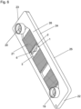
- the flow inverter 1 comprises a first plate 2 and a second plate 3.
- the second plate 3 and the first plate 2 are arranged consecutively adjacent to one another along an extension direction D, in the order indicated.
- a first wall 4 is arranged on the first plate 2, e.g. an edge of the first plate 2, in two side regions 13 of the flow inverter 1 from a first main side and on the second plate 3, e.g. an edge of the second plate 3, in a central region 12 from a second main side.
- a second wall 5 is arranged on the second plate 3 in the side regions 13 of the flow inverter 1 and on the first plate 2 in the central region 12 of the flow inverter 1.
- the first plate 2 has a first side surface 8 and a second side surface 9 and the second plate 3 has a first side surface 10 and a second side surface 11.
- the first side surface 8 and the second side surface 9 of the first plate 2 are arranged opposite to one another.
- the first side surface 10 and the second side surface 11 of the second plate 3 are arranged opposite to one another.
- the first side surface of the first plate 8 and the first side surface of the second plate 10 form a first side surface of the flow inverter 1.
- the second side surface of the first plate 9 and the second side surface of the second plate 11 form a second side surface of the flow inverter 1. Both the first side surface of the flow inverter 1 and the second side surface of the flow inverter 1 extend along the extension direction D.
- the first wall 4 completely extends from the first side surface of the first plate 8 to the second side surface of the first plate 9. Furthermore, the second wall 5 completely extends from the first side surface of the second plate 10 to the second side surface of the second plate 11.
- the first wall 4 comprises four first partial walls 14, wherein directly adjacent first partial walls 14 are directly connected to one another, e.g. being formed in one piece. Directly adjacent first partial walls 14 enclose an angle with one another. Here, the enclosing angles are all the same.
- the first wall 4 has a first curved shape in plan view. In this exemplary embodiment, the first curved shape is half of an octagon. An outer surface of the first curved shape 30 points in the direction of the second plate 3.
- a first recess 6 is provided between the first plate 2 and the second plate 3 in the central region 12.
- the first recess 6 completely penetrates the second plate 3 in the central region 12.
- two second recesses 7 are provided between the first plate 2 and the second plate 3. Each of the two second recesses 7 completely penetrates the first plate 2 in the side regions 13.
- the first recess 6 is provided between the two second recesses 7 perpendicular to the extension direction D.
- the first wall 4 and the second wall 5 overlap at least partly with one another in plan view, delimiting the first recess 6 and the two second recesses 7 at least partly.
- the first recess 6 is delimited by the first wall 4 and the second wall 5 in the central region 12.
- the second wall 5 comprises three second partial walls 15, wherein directly adjacent second partial walls 15 are directly connected to one another, e.g. being formed in one piece. Directly adjacent second partial walls 15 enclose an angle with one another.
- the enclosing angles are all the same.
- the second wall 5 has a second curved shape in plan view. An outer surface of the second curved shape 31 points in the direction of the first plate 2.
- each second recess 7 is delimited by the first wall 4 and the second wall 5 in the respective side region 13 and by the projection of the outer surface of the flow inverter in plan view.
- the flow inverter 1 according to Figures 3 and 4 comprises the first plate 2 and the second plate 3, wherein the first plate 2 and the second plate 3 extend in a common plane.
- the first wall 4 and the second wall 5 each extend in a direction perpendicular to the extension direction D of the flow inverter 1.
- the first plate 2 and the second plate 3 as well as the first wall 4 and the second wall 5 are formed in one piece, for example.
- the power semiconductor component 16 of Figure 5 comprises three power semiconductor modules 17, each being connected to a cooling structure 21, wherein each cooling structure 21 is part, e.g. an integral part, of a respective power semiconductor module 17.
- the power semiconductor modules 17 are provided on and the respective cooling structure 21 are provided in a cooling chamber (not shown in Figure 5 ) being described more detailed in connection with Figure 6 .
- the cooling chamber has an inlet port 19 and an outlet port 20 (not shown in Figure 5 ) described in more detail in connection with Figure 6 .
- the cooling chamber is adapted for a flow direction FD of a coolant substance 18 within the cooling chamber from the inlet port 19 to the outlet port 20.
- the power semiconductor modules 17 are provided on the cooling chamber consecutively along the flow direction FD.
- each of the cooling structures 21 are provided within the cooling chamber consecutively in the direction of the flow direction FD.
- the flow inverter 1 according to Figures 1 to 4 is provided in the cooling chamber between two of the at least two cooling structures 21.
- a region where the flow inverter 1 is arranged is indicated in Figure 5 by two dashed lines. Within the two dashed lines, the flow inverter 1 is arranged.
- the flow inverter 1 is arranged between directly neighbouring power semiconductor modules 17 closest to the outlet port 20.
- the coolant substance 18 has a first average temperature in a top part X of the cooling chamber in flow direction FD before the flow inverter 1 and a second average temperature in the bottom part X' of the cooling chamber in flow direction FD before the flow inverter 1.
- the average first average temperature is higher than the average second average temperature since the cooling structures 21 dissipate more heat to the coolant substance 18 in the top part X.
- the flow inverter 1 inverts the coolant substance 18 after the flow inverter 1 in flow direction FD in vertical direction.
- the portion of the coolant substance of the top part X is redirected to a bottom part Y' of the cooling chamber in flow direction FD after the flow inverter 1 and the portion of the coolant substance of the bottom part X' is redirected to a top part Y of the cooling chamber in flow direction FD after the flow inverter 1.
- the power semiconductor module 17 closest to the outlet port 20 can be cooled down effectively.
- the power semiconductor component 16 of Figure 6 has a cooling chamber comprising a cover 25, two sidewalls 24, a front 22, a back 23 and a bottom 26 forming a cooling cavity.
- the cooling structures 21 are located within the cooling cavity.
- the flow inverter 1 is arranged as already described in connection with Figure 5 between directly neighbouring cooling structures 21 closest to the outlet port 20.
- the second plate 3 faces the inlet port 19 and the first plate 2 faces the outlet port 20.
Landscapes
- Engineering & Computer Science (AREA)
- Physics & Mathematics (AREA)
- Thermal Sciences (AREA)
- Mechanical Engineering (AREA)
- General Engineering & Computer Science (AREA)
- Cooling Or The Like Of Semiconductors Or Solid State Devices (AREA)
Claims (15)
- Inverseur de flux (1) pour une substance de refroidissement (18) pour un composant semiconducteur de puissance (16) avec au moins deux modules semiconducteurs de puissance (17) et une chambre de refroidissement, comprenant- une première plaque (2) s'étendant le long d'un plan d'étendue principal de l'inverseur de flux (1),- une seconde plaque (3) s'étendant le long du plan d'étendue principal,- une première paroi (4) placée sur la première plaque (2) et la seconde plaque (3) et s'étendant depuis un premier côté principal de l'inverseur de flux (1), et- une seconde paroi (5) placée sur la première plaque (2) et la seconde plaque (3) et s'étendant depuis un second côté principal de l'inverseur de flux (1) opposé au premier côté principal, dans lequel- la première plaque (2) est placée à côté de la seconde plaque (3),- au moins un premier renfoncement (6) est formé entre la première plaque (2) et la seconde plaque (3), et- au moins un second renfoncement (7) est formé entre la première plaque (2) et la seconde plaque (3).
- Inverseur de flux (1) selon la revendication 1, dans lequel- l'au moins un premier renfoncement (6) est formé dans une région centrale (12) de l'inverseur de flux (1), et- l'au moins un second renfoncement (7) est formé dans au moins une région latérale (13) de l'inverseur de flux (1) .
- Inverseur de flux (1) selon l'une ou l'autre des revendications 1 et 2, dans lequel la première plaque (2) et la seconde plaque (3) s'étendent parallèlement l'une à l'autre.
- Inverseur de flux (1) selon l'une quelconque des revendications 1 à 3, dans lequel- la première paroi (4) s'étend complètement le long d'une largeur de la première plaque (2), et- la seconde paroi (5) s'étend complètement le long d'une largeur de la seconde plaque (3).
- Inverseur de flux (1) selon l'une quelconque des revendications 1 à 3, dans lequel- la première paroi (4) présente une première forme incurvée dans une vue en plan et une surface extérieure de la première forme incurvée pointe en direction de la seconde plaque (3), et/ou- la seconde paroi (5) présente une seconde forme incurvée dans une vue en plan et une surface extérieure de la seconde forme incurvée pointe en direction de la première plaque (2).
- Inverseur de flux (1) selon l'une quelconque des revendications 1 à 5, dans lequel deux seconds renfoncements (7) sont formés entre la première plaque (2) et la seconde plaque (3) dans deux régions latérales opposées (13) de l'inverseur de flux (1).
- Inverseur de flux (1) selon la revendication 6, dans lequel le premier renfoncement (6) est formé entre les deux seconds renfoncements (7).
- Inverseur de flux (1) selon l'une quelconque des revendications 1 à 7, dans lequel la première paroi (4) et la seconde paroi (5) se chevauchent l'une l'autre au moins partiellement dans une vue en plan et délimitent ainsi le premier renfoncement (6) et l'au moins un second renfoncement (7) au moins partiellement.
- Inverseur de flux (1) selon l'une quelconque des revendications 1 à 8, dans lequel- le premier renfoncement (6) est placé sur un côté de la première paroi (4) orienté vers la première plaque (2),- l'au moins un second renfoncement (7) est placé sur un côté de la première paroi (4) orienté vers la seconde plaque (3).
- Composant semiconducteur de puissance (16), comprenant- au moins deux modules semiconducteurs de puissance (17), raccordés chacun à une structure de refroidissement (21) respective, et- une chambre de refroidissement comportant un orifice d'entrée (19) et un orifice de sortie (20), dans lequel- la chambre de refroidissement est conçue pour un sens d'écoulement (FD) d'une substance de refroidissement (18) à l'intérieur de la chambre de refroidissement de l'orifice d'entrée (19) à l'orifice de sortie (20),- les au moins deux structures de refroidissement (21) sont placées à l'intérieur de la chambre de refroidissement de manière successive dans le sens d'écoulement (FD),- la chambre de refroidissement comprend un inverseur de flux (1) selon l'une quelconque des revendications 1 à 9 placé entre deux des au moins deux structures de refroidissement (21).
- Composant semiconducteur de puissance (16) selon la revendication 10, dans lequel- l'inverseur de flux (1) est un inverseur de flux (1) selon l'une quelconque des revendications 1 à 9,- la première plaque (2) est située plus près de l'orifice de sortie (20), et- la seconde plaque (3) est située plus près de l'orifice d'entrée (19).
- Composant semiconducteur de puissance (16) selon l'une ou l'autre des revendications 10 et 11, dans lequel- la première plaque (2) s'étend parallèlement à une partie de recouvrement et une partie inférieure de la chambre de refroidissement, et/ou- la seconde plaque (3) s'étend parallèlement à une partie de recouvrement et une partie inférieure de la chambre de refroidissement, et/ou- la première paroi (4) s'étend perpendiculairement à une partie de recouvrement de la chambre de refroidissement, et/ou- la seconde paroi (5) s'étend perpendiculairement à une partie inférieure de la chambre de refroidissement.
- Composant semiconducteur de puissance (16) selon l'une quelconque des revendications 10 à 12, dans lequel- la première paroi (4) s'étend d'une première surface latérale de la chambre de refroidissement à une seconde surface latérale de la chambre de refroidissement, et- la seconde paroi (5) s'étend de la première surface latérale de la chambre de refroidissement à la seconde surface latérale de la chambre de refroidissement.
- Procédé de production d'un composant semiconducteur de puissance (16), comprenant- préparer au moins deux modules semiconducteurs de puissance (17), raccordés chacun à une structure de refroidissement (21) respective, et- préparer une chambre de refroidissement comportant un orifice d'entrée (19) et un orifice de sortie (20),- disposer les au moins deux modules semiconducteurs de puissance (17) sur la chambre de refroidissement, et- disposer un inverseur de flux selon l'une quelconque des revendications 1 à 9 entre deux des au moins deux structures de refroidissement (21).
- Procédé selon la revendication 14, dans lequel l'inverseur de flux (1) est disposé dans la chambre de refroidissement par soudage, brasage tendre, serrage, brasage fort, collage et/ou insertion sous forme de pièce séparée.
Priority Applications (5)
| Application Number | Priority Date | Filing Date | Title |
|---|---|---|---|
| EP21214313.5A EP4199077B1 (fr) | 2021-12-14 | 2021-12-14 | Inverseur de flux et composant semi-conducteur de puissance |
| CN202280076400.3A CN118266074B (zh) | 2021-12-14 | 2022-12-01 | 转流器和功率半导体部件 |
| JP2024535510A JP7610763B2 (ja) | 2021-12-14 | 2022-12-01 | フローインバータおよびパワー半導体構成要素 |
| US18/719,794 US20250054836A1 (en) | 2021-12-14 | 2022-12-01 | Flow inverter and power semiconductor component |
| PCT/EP2022/084041 WO2023110431A1 (fr) | 2021-12-14 | 2022-12-01 | Onduleur d'écoulement à composant semi-conducteur de puissance |
Applications Claiming Priority (1)
| Application Number | Priority Date | Filing Date | Title |
|---|---|---|---|
| EP21214313.5A EP4199077B1 (fr) | 2021-12-14 | 2021-12-14 | Inverseur de flux et composant semi-conducteur de puissance |
Publications (2)
| Publication Number | Publication Date |
|---|---|
| EP4199077A1 EP4199077A1 (fr) | 2023-06-21 |
| EP4199077B1 true EP4199077B1 (fr) | 2024-02-07 |
Family
ID=79687052
Family Applications (1)
| Application Number | Title | Priority Date | Filing Date |
|---|---|---|---|
| EP21214313.5A Active EP4199077B1 (fr) | 2021-12-14 | 2021-12-14 | Inverseur de flux et composant semi-conducteur de puissance |
Country Status (5)
| Country | Link |
|---|---|
| US (1) | US20250054836A1 (fr) |
| EP (1) | EP4199077B1 (fr) |
| JP (1) | JP7610763B2 (fr) |
| CN (1) | CN118266074B (fr) |
| WO (1) | WO2023110431A1 (fr) |
Family Cites Families (9)
| Publication number | Priority date | Publication date | Assignee | Title |
|---|---|---|---|---|
| JPH0333070Y2 (fr) * | 1985-02-08 | 1991-07-12 | ||
| JP2584772Y2 (ja) * | 1992-08-28 | 1998-11-05 | 東洋ラジエーター株式会社 | ヒートシンク構造 |
| JP3982180B2 (ja) * | 2000-02-16 | 2007-09-26 | 株式会社日立製作所 | 電力変換装置 |
| JP2002315357A (ja) * | 2001-04-16 | 2002-10-25 | Hitachi Ltd | インバータ装置 |
| JP4881583B2 (ja) * | 2005-06-27 | 2012-02-22 | 株式会社豊田自動織機 | パワーモジュール用ヒートシンク |
| US7834448B2 (en) * | 2007-09-05 | 2010-11-16 | Delphi Technologies, Inc. | Fluid cooled semiconductor power module having double-sided cooling |
| JP4766110B2 (ja) * | 2008-01-10 | 2011-09-07 | 株式会社デンソー | 半導体冷却構造 |
| JP2012033966A (ja) | 2011-10-31 | 2012-02-16 | Toyota Industries Corp | パワーモジュール用ヒートシンク |
| DE102019202902A1 (de) * | 2019-03-04 | 2020-09-10 | Abb Schweiz Ag | Direkte Kühlung eines Stromrichters durch Verwendung einer geprägten Platte |
-
2021
- 2021-12-14 EP EP21214313.5A patent/EP4199077B1/fr active Active
-
2022
- 2022-12-01 WO PCT/EP2022/084041 patent/WO2023110431A1/fr not_active Ceased
- 2022-12-01 CN CN202280076400.3A patent/CN118266074B/zh active Active
- 2022-12-01 US US18/719,794 patent/US20250054836A1/en active Pending
- 2022-12-01 JP JP2024535510A patent/JP7610763B2/ja active Active
Also Published As
| Publication number | Publication date |
|---|---|
| CN118266074A (zh) | 2024-06-28 |
| WO2023110431A1 (fr) | 2023-06-22 |
| JP7610763B2 (ja) | 2025-01-08 |
| JP2024545221A (ja) | 2024-12-05 |
| EP4199077A1 (fr) | 2023-06-21 |
| CN118266074B (zh) | 2025-11-25 |
| US20250054836A1 (en) | 2025-02-13 |
Similar Documents
| Publication | Publication Date | Title |
|---|---|---|
| KR101906646B1 (ko) | 반도체 모듈용 냉각기 및 반도체 모듈 | |
| JP6512266B2 (ja) | 半導体装置 | |
| JP6093186B2 (ja) | 半導体モジュール用冷却器 | |
| EP3573097B1 (fr) | Appareil de refroidissement, module semiconducteur, véhicule et procédé de fabrication | |
| JP5565459B2 (ja) | 半導体モジュール及び冷却器 | |
| EP3905318A1 (fr) | Ensemble module d'alimentation | |
| JP4766110B2 (ja) | 半導体冷却構造 | |
| US10756001B2 (en) | Semiconductor module | |
| JP7160216B2 (ja) | 半導体装置 | |
| JP7537199B2 (ja) | 放熱器、冷却装置 | |
| JP2011071398A (ja) | 半導体冷却構造 | |
| JP7205662B2 (ja) | 半導体モジュール | |
| JP3685170B2 (ja) | 冷却装置 | |
| KR20210088329A (ko) | 전력 모듈 | |
| WO2020031753A1 (fr) | Refroidisseur et module à semi-conducteur | |
| JPWO2021256083A5 (fr) | ||
| US20250054836A1 (en) | Flow inverter and power semiconductor component | |
| CA1146282A (fr) | Capsule dissipatrice de chaleur pour composants semiconducteurs en forme de disque | |
| JP2023548625A (ja) | パワー半導体コンポーネント | |
| CN116895616A (zh) | 冷却装置 | |
| CN116110862A (zh) | 一种散热器及功率模块 | |
| KR20250148187A (ko) | 냉각 플레이트 조립체 및 이를 포함하는 배터리 모듈 | |
| JP7407577B2 (ja) | ヒートシンク | |
| WO2025204327A1 (fr) | Échangeur de chaleur de refroidissement | |
| CN121769641A (zh) | 一种散热组件及半导体激光器组件 |
Legal Events
| Date | Code | Title | Description |
|---|---|---|---|
| PUAI | Public reference made under article 153(3) epc to a published international application that has entered the european phase |
Free format text: ORIGINAL CODE: 0009012 |
|
| STAA | Information on the status of an ep patent application or granted ep patent |
Free format text: STATUS: REQUEST FOR EXAMINATION WAS MADE |
|
| 17P | Request for examination filed |
Effective date: 20220803 |
|
| AK | Designated contracting states |
Kind code of ref document: A1 Designated state(s): AL AT BE BG CH CY CZ DE DK EE ES FI FR GB GR HR HU IE IS IT LI LT LU LV MC MK MT NL NO PL PT RO RS SE SI SK SM TR |
|
| RIC1 | Information provided on ipc code assigned before grant |
Ipc: H01L 25/11 20060101ALI20230705BHEP Ipc: H01L 25/00 20060101ALI20230705BHEP Ipc: H01L 23/367 20060101ALI20230705BHEP Ipc: H01L 23/46 20060101AFI20230705BHEP |
|
| GRAP | Despatch of communication of intention to grant a patent |
Free format text: ORIGINAL CODE: EPIDOSNIGR1 |
|
| STAA | Information on the status of an ep patent application or granted ep patent |
Free format text: STATUS: GRANT OF PATENT IS INTENDED |
|
| INTG | Intention to grant announced |
Effective date: 20230823 |
|
| RAP1 | Party data changed (applicant data changed or rights of an application transferred) |
Owner name: HITACHI ENERGY LTD |
|
| GRAS | Grant fee paid |
Free format text: ORIGINAL CODE: EPIDOSNIGR3 |
|
| P01 | Opt-out of the competence of the unified patent court (upc) registered |
Effective date: 20231129 |
|
| GRAA | (expected) grant |
Free format text: ORIGINAL CODE: 0009210 |
|
| STAA | Information on the status of an ep patent application or granted ep patent |
Free format text: STATUS: THE PATENT HAS BEEN GRANTED |
|
| AK | Designated contracting states |
Kind code of ref document: B1 Designated state(s): AL AT BE BG CH CY CZ DE DK EE ES FI FR GB GR HR HU IE IS IT LI LT LU LV MC MK MT NL NO PL PT RO RS SE SI SK SM TR |
|
| REG | Reference to a national code |
Ref country code: GB Ref legal event code: FG4D |
|
| REG | Reference to a national code |
Ref country code: CH Ref legal event code: EP |
|
| REG | Reference to a national code |
Ref country code: DE Ref legal event code: R096 Ref document number: 602021009199 Country of ref document: DE |
|
| REG | Reference to a national code |
Ref country code: IE Ref legal event code: FG4D |
|
| REG | Reference to a national code |
Ref country code: LT Ref legal event code: MG9D |
|
| REG | Reference to a national code |
Ref country code: NL Ref legal event code: MP Effective date: 20240207 |
|
| PG25 | Lapsed in a contracting state [announced via postgrant information from national office to epo] |
Ref country code: IS Free format text: LAPSE BECAUSE OF FAILURE TO SUBMIT A TRANSLATION OF THE DESCRIPTION OR TO PAY THE FEE WITHIN THE PRESCRIBED TIME-LIMIT Effective date: 20240607 |
|
| PG25 | Lapsed in a contracting state [announced via postgrant information from national office to epo] |
Ref country code: LT Free format text: LAPSE BECAUSE OF FAILURE TO SUBMIT A TRANSLATION OF THE DESCRIPTION OR TO PAY THE FEE WITHIN THE PRESCRIBED TIME-LIMIT Effective date: 20240207 |
|
| PG25 | Lapsed in a contracting state [announced via postgrant information from national office to epo] |
Ref country code: GR Free format text: LAPSE BECAUSE OF FAILURE TO SUBMIT A TRANSLATION OF THE DESCRIPTION OR TO PAY THE FEE WITHIN THE PRESCRIBED TIME-LIMIT Effective date: 20240508 |
|
| REG | Reference to a national code |
Ref country code: AT Ref legal event code: MK05 Ref document number: 1655921 Country of ref document: AT Kind code of ref document: T Effective date: 20240207 |
|
| PG25 | Lapsed in a contracting state [announced via postgrant information from national office to epo] |
Ref country code: HR Free format text: LAPSE BECAUSE OF FAILURE TO SUBMIT A TRANSLATION OF THE DESCRIPTION OR TO PAY THE FEE WITHIN THE PRESCRIBED TIME-LIMIT Effective date: 20240207 Ref country code: RS Free format text: LAPSE BECAUSE OF FAILURE TO SUBMIT A TRANSLATION OF THE DESCRIPTION OR TO PAY THE FEE WITHIN THE PRESCRIBED TIME-LIMIT Effective date: 20240507 Ref country code: NL Free format text: LAPSE BECAUSE OF FAILURE TO SUBMIT A TRANSLATION OF THE DESCRIPTION OR TO PAY THE FEE WITHIN THE PRESCRIBED TIME-LIMIT Effective date: 20240207 |
|
| PG25 | Lapsed in a contracting state [announced via postgrant information from national office to epo] |
Ref country code: ES Free format text: LAPSE BECAUSE OF FAILURE TO SUBMIT A TRANSLATION OF THE DESCRIPTION OR TO PAY THE FEE WITHIN THE PRESCRIBED TIME-LIMIT Effective date: 20240207 |
|
| PG25 | Lapsed in a contracting state [announced via postgrant information from national office to epo] |
Ref country code: AT Free format text: LAPSE BECAUSE OF FAILURE TO SUBMIT A TRANSLATION OF THE DESCRIPTION OR TO PAY THE FEE WITHIN THE PRESCRIBED TIME-LIMIT Effective date: 20240207 |
|
| PG25 | Lapsed in a contracting state [announced via postgrant information from national office to epo] |
Ref country code: RS Free format text: LAPSE BECAUSE OF FAILURE TO SUBMIT A TRANSLATION OF THE DESCRIPTION OR TO PAY THE FEE WITHIN THE PRESCRIBED TIME-LIMIT Effective date: 20240507 Ref country code: NO Free format text: LAPSE BECAUSE OF FAILURE TO SUBMIT A TRANSLATION OF THE DESCRIPTION OR TO PAY THE FEE WITHIN THE PRESCRIBED TIME-LIMIT Effective date: 20240507 Ref country code: NL Free format text: LAPSE BECAUSE OF FAILURE TO SUBMIT A TRANSLATION OF THE DESCRIPTION OR TO PAY THE FEE WITHIN THE PRESCRIBED TIME-LIMIT Effective date: 20240207 Ref country code: LT Free format text: LAPSE BECAUSE OF FAILURE TO SUBMIT A TRANSLATION OF THE DESCRIPTION OR TO PAY THE FEE WITHIN THE PRESCRIBED TIME-LIMIT Effective date: 20240207 Ref country code: IS Free format text: LAPSE BECAUSE OF FAILURE TO SUBMIT A TRANSLATION OF THE DESCRIPTION OR TO PAY THE FEE WITHIN THE PRESCRIBED TIME-LIMIT Effective date: 20240607 Ref country code: HR Free format text: LAPSE BECAUSE OF FAILURE TO SUBMIT A TRANSLATION OF THE DESCRIPTION OR TO PAY THE FEE WITHIN THE PRESCRIBED TIME-LIMIT Effective date: 20240207 Ref country code: GR Free format text: LAPSE BECAUSE OF FAILURE TO SUBMIT A TRANSLATION OF THE DESCRIPTION OR TO PAY THE FEE WITHIN THE PRESCRIBED TIME-LIMIT Effective date: 20240508 Ref country code: FI Free format text: LAPSE BECAUSE OF FAILURE TO SUBMIT A TRANSLATION OF THE DESCRIPTION OR TO PAY THE FEE WITHIN THE PRESCRIBED TIME-LIMIT Effective date: 20240207 Ref country code: ES Free format text: LAPSE BECAUSE OF FAILURE TO SUBMIT A TRANSLATION OF THE DESCRIPTION OR TO PAY THE FEE WITHIN THE PRESCRIBED TIME-LIMIT Effective date: 20240207 Ref country code: BG Free format text: LAPSE BECAUSE OF FAILURE TO SUBMIT A TRANSLATION OF THE DESCRIPTION OR TO PAY THE FEE WITHIN THE PRESCRIBED TIME-LIMIT Effective date: 20240207 Ref country code: AT Free format text: LAPSE BECAUSE OF FAILURE TO SUBMIT A TRANSLATION OF THE DESCRIPTION OR TO PAY THE FEE WITHIN THE PRESCRIBED TIME-LIMIT Effective date: 20240207 |
|
| PG25 | Lapsed in a contracting state [announced via postgrant information from national office to epo] |
Ref country code: PT Free format text: LAPSE BECAUSE OF FAILURE TO SUBMIT A TRANSLATION OF THE DESCRIPTION OR TO PAY THE FEE WITHIN THE PRESCRIBED TIME-LIMIT Effective date: 20240607 Ref country code: PL Free format text: LAPSE BECAUSE OF FAILURE TO SUBMIT A TRANSLATION OF THE DESCRIPTION OR TO PAY THE FEE WITHIN THE PRESCRIBED TIME-LIMIT Effective date: 20240207 |
|
| PG25 | Lapsed in a contracting state [announced via postgrant information from national office to epo] |
Ref country code: SE Free format text: LAPSE BECAUSE OF FAILURE TO SUBMIT A TRANSLATION OF THE DESCRIPTION OR TO PAY THE FEE WITHIN THE PRESCRIBED TIME-LIMIT Effective date: 20240207 Ref country code: PT Free format text: LAPSE BECAUSE OF FAILURE TO SUBMIT A TRANSLATION OF THE DESCRIPTION OR TO PAY THE FEE WITHIN THE PRESCRIBED TIME-LIMIT Effective date: 20240607 Ref country code: PL Free format text: LAPSE BECAUSE OF FAILURE TO SUBMIT A TRANSLATION OF THE DESCRIPTION OR TO PAY THE FEE WITHIN THE PRESCRIBED TIME-LIMIT Effective date: 20240207 Ref country code: LV Free format text: LAPSE BECAUSE OF FAILURE TO SUBMIT A TRANSLATION OF THE DESCRIPTION OR TO PAY THE FEE WITHIN THE PRESCRIBED TIME-LIMIT Effective date: 20240207 |
|
| PG25 | Lapsed in a contracting state [announced via postgrant information from national office to epo] |
Ref country code: DK Free format text: LAPSE BECAUSE OF FAILURE TO SUBMIT A TRANSLATION OF THE DESCRIPTION OR TO PAY THE FEE WITHIN THE PRESCRIBED TIME-LIMIT Effective date: 20240207 |
|
| PG25 | Lapsed in a contracting state [announced via postgrant information from national office to epo] |
Ref country code: SM Free format text: LAPSE BECAUSE OF FAILURE TO SUBMIT A TRANSLATION OF THE DESCRIPTION OR TO PAY THE FEE WITHIN THE PRESCRIBED TIME-LIMIT Effective date: 20240207 |
|
| PG25 | Lapsed in a contracting state [announced via postgrant information from national office to epo] |
Ref country code: CZ Free format text: LAPSE BECAUSE OF FAILURE TO SUBMIT A TRANSLATION OF THE DESCRIPTION OR TO PAY THE FEE WITHIN THE PRESCRIBED TIME-LIMIT Effective date: 20240207 Ref country code: EE Free format text: LAPSE BECAUSE OF FAILURE TO SUBMIT A TRANSLATION OF THE DESCRIPTION OR TO PAY THE FEE WITHIN THE PRESCRIBED TIME-LIMIT Effective date: 20240207 |
|
| PG25 | Lapsed in a contracting state [announced via postgrant information from national office to epo] |
Ref country code: SK Free format text: LAPSE BECAUSE OF FAILURE TO SUBMIT A TRANSLATION OF THE DESCRIPTION OR TO PAY THE FEE WITHIN THE PRESCRIBED TIME-LIMIT Effective date: 20240207 |
|
| PG25 | Lapsed in a contracting state [announced via postgrant information from national office to epo] |
Ref country code: SM Free format text: LAPSE BECAUSE OF FAILURE TO SUBMIT A TRANSLATION OF THE DESCRIPTION OR TO PAY THE FEE WITHIN THE PRESCRIBED TIME-LIMIT Effective date: 20240207 Ref country code: SK Free format text: LAPSE BECAUSE OF FAILURE TO SUBMIT A TRANSLATION OF THE DESCRIPTION OR TO PAY THE FEE WITHIN THE PRESCRIBED TIME-LIMIT Effective date: 20240207 Ref country code: RO Free format text: LAPSE BECAUSE OF FAILURE TO SUBMIT A TRANSLATION OF THE DESCRIPTION OR TO PAY THE FEE WITHIN THE PRESCRIBED TIME-LIMIT Effective date: 20240207 Ref country code: EE Free format text: LAPSE BECAUSE OF FAILURE TO SUBMIT A TRANSLATION OF THE DESCRIPTION OR TO PAY THE FEE WITHIN THE PRESCRIBED TIME-LIMIT Effective date: 20240207 Ref country code: DK Free format text: LAPSE BECAUSE OF FAILURE TO SUBMIT A TRANSLATION OF THE DESCRIPTION OR TO PAY THE FEE WITHIN THE PRESCRIBED TIME-LIMIT Effective date: 20240207 Ref country code: CZ Free format text: LAPSE BECAUSE OF FAILURE TO SUBMIT A TRANSLATION OF THE DESCRIPTION OR TO PAY THE FEE WITHIN THE PRESCRIBED TIME-LIMIT Effective date: 20240207 |
|
| REG | Reference to a national code |
Ref country code: DE Ref legal event code: R097 Ref document number: 602021009199 Country of ref document: DE |
|
| PG25 | Lapsed in a contracting state [announced via postgrant information from national office to epo] |
Ref country code: IT Free format text: LAPSE BECAUSE OF FAILURE TO SUBMIT A TRANSLATION OF THE DESCRIPTION OR TO PAY THE FEE WITHIN THE PRESCRIBED TIME-LIMIT Effective date: 20240207 |
|
| PLBE | No opposition filed within time limit |
Free format text: ORIGINAL CODE: 0009261 |
|
| STAA | Information on the status of an ep patent application or granted ep patent |
Free format text: STATUS: NO OPPOSITION FILED WITHIN TIME LIMIT |
|
| PG25 | Lapsed in a contracting state [announced via postgrant information from national office to epo] |
Ref country code: IT Free format text: LAPSE BECAUSE OF FAILURE TO SUBMIT A TRANSLATION OF THE DESCRIPTION OR TO PAY THE FEE WITHIN THE PRESCRIBED TIME-LIMIT Effective date: 20240207 |
|
| 26N | No opposition filed |
Effective date: 20241108 |
|
| PG25 | Lapsed in a contracting state [announced via postgrant information from national office to epo] |
Ref country code: SI Free format text: LAPSE BECAUSE OF FAILURE TO SUBMIT A TRANSLATION OF THE DESCRIPTION OR TO PAY THE FEE WITHIN THE PRESCRIBED TIME-LIMIT Effective date: 20240207 |
|
| PG25 | Lapsed in a contracting state [announced via postgrant information from national office to epo] |
Ref country code: MC Free format text: LAPSE BECAUSE OF FAILURE TO SUBMIT A TRANSLATION OF THE DESCRIPTION OR TO PAY THE FEE WITHIN THE PRESCRIBED TIME-LIMIT Effective date: 20240207 |
|
| REG | Reference to a national code |
Ref country code: CH Ref legal event code: PL |
|
| PG25 | Lapsed in a contracting state [announced via postgrant information from national office to epo] |
Ref country code: LU Free format text: LAPSE BECAUSE OF NON-PAYMENT OF DUE FEES Effective date: 20241214 |
|
| REG | Reference to a national code |
Ref country code: BE Ref legal event code: MM Effective date: 20241231 |
|
| PG25 | Lapsed in a contracting state [announced via postgrant information from national office to epo] |
Ref country code: BE Free format text: LAPSE BECAUSE OF NON-PAYMENT OF DUE FEES Effective date: 20241231 |
|
| PG25 | Lapsed in a contracting state [announced via postgrant information from national office to epo] |
Ref country code: FR Free format text: LAPSE BECAUSE OF NON-PAYMENT OF DUE FEES Effective date: 20241231 |
|
| PG25 | Lapsed in a contracting state [announced via postgrant information from national office to epo] |
Ref country code: CH Free format text: LAPSE BECAUSE OF NON-PAYMENT OF DUE FEES Effective date: 20241231 |
|
| PG25 | Lapsed in a contracting state [announced via postgrant information from national office to epo] |
Ref country code: IE Free format text: LAPSE BECAUSE OF NON-PAYMENT OF DUE FEES Effective date: 20241214 |
|
| REG | Reference to a national code |
Ref country code: DE Ref legal event code: R079 Ref document number: 602021009199 Country of ref document: DE Free format text: PREVIOUS MAIN CLASS: H01L0023460000 Ipc: H10W0040400000 |
|
| PGFP | Annual fee paid to national office [announced via postgrant information from national office to epo] |
Ref country code: DE Payment date: 20251211 Year of fee payment: 5 |
|
| PGFP | Annual fee paid to national office [announced via postgrant information from national office to epo] |
Ref country code: GB Payment date: 20251219 Year of fee payment: 5 |
|
| PG25 | Lapsed in a contracting state [announced via postgrant information from national office to epo] |
Ref country code: CY Free format text: LAPSE BECAUSE OF FAILURE TO SUBMIT A TRANSLATION OF THE DESCRIPTION OR TO PAY THE FEE WITHIN THE PRESCRIBED TIME-LIMIT Effective date: 20240207 |