EP4199089A1 - Structure semi-conductrice et procédé de fabrication associé - Google Patents
Structure semi-conductrice et procédé de fabrication associé Download PDFInfo
- Publication number
- EP4199089A1 EP4199089A1 EP22715511.6A EP22715511A EP4199089A1 EP 4199089 A1 EP4199089 A1 EP 4199089A1 EP 22715511 A EP22715511 A EP 22715511A EP 4199089 A1 EP4199089 A1 EP 4199089A1
- Authority
- EP
- European Patent Office
- Prior art keywords
- layers
- semiconductor
- initial
- area
- dielectric layer
- Prior art date
- Legal status (The legal status is an assumption and is not a legal conclusion. Google has not performed a legal analysis and makes no representation as to the accuracy of the status listed.)
- Pending
Links
Images




Classifications
-
- H—ELECTRICITY
- H10—SEMICONDUCTOR DEVICES; ELECTRIC SOLID-STATE DEVICES NOT OTHERWISE PROVIDED FOR
- H10B—ELECTRONIC MEMORY DEVICES
- H10B12/00—Dynamic random access memory [DRAM] devices
- H10B12/01—Manufacture or treatment
- H10B12/02—Manufacture or treatment for one transistor one-capacitor [1T-1C] memory cells
- H10B12/05—Making the transistor
-
- H—ELECTRICITY
- H10—SEMICONDUCTOR DEVICES; ELECTRIC SOLID-STATE DEVICES NOT OTHERWISE PROVIDED FOR
- H10B—ELECTRONIC MEMORY DEVICES
- H10B12/00—Dynamic random access memory [DRAM] devices
- H10B12/30—DRAM devices comprising one-transistor - one-capacitor [1T-1C] memory cells
- H10B12/31—DRAM devices comprising one-transistor - one-capacitor [1T-1C] memory cells having a storage electrode stacked over the transistor
- H10B12/315—DRAM devices comprising one-transistor - one-capacitor [1T-1C] memory cells having a storage electrode stacked over the transistor with the capacitor higher than a bit line
-
- H—ELECTRICITY
- H10—SEMICONDUCTOR DEVICES; ELECTRIC SOLID-STATE DEVICES NOT OTHERWISE PROVIDED FOR
- H10B—ELECTRONIC MEMORY DEVICES
- H10B12/00—Dynamic random access memory [DRAM] devices
- H10B12/30—DRAM devices comprising one-transistor - one-capacitor [1T-1C] memory cells
- H10B12/34—DRAM devices comprising one-transistor - one-capacitor [1T-1C] memory cells the transistor being at least partially in a trench in the substrate
-
- H—ELECTRICITY
- H10—SEMICONDUCTOR DEVICES; ELECTRIC SOLID-STATE DEVICES NOT OTHERWISE PROVIDED FOR
- H10B—ELECTRONIC MEMORY DEVICES
- H10B12/00—Dynamic random access memory [DRAM] devices
- H10B12/30—DRAM devices comprising one-transistor - one-capacitor [1T-1C] memory cells
- H10B12/48—Data lines or contacts therefor
- H10B12/482—Bit lines
-
- H—ELECTRICITY
- H10—SEMICONDUCTOR DEVICES; ELECTRIC SOLID-STATE DEVICES NOT OTHERWISE PROVIDED FOR
- H10D—INORGANIC ELECTRIC SEMICONDUCTOR DEVICES
- H10D30/00—Field-effect transistors [FET]
- H10D30/01—Manufacture or treatment
- H10D30/021—Manufacture or treatment of FETs having insulated gates [IGFET]
- H10D30/031—Manufacture or treatment of FETs having insulated gates [IGFET] of thin-film transistors [TFT]
-
- H—ELECTRICITY
- H10—SEMICONDUCTOR DEVICES; ELECTRIC SOLID-STATE DEVICES NOT OTHERWISE PROVIDED FOR
- H10D—INORGANIC ELECTRIC SEMICONDUCTOR DEVICES
- H10D30/00—Field-effect transistors [FET]
- H10D30/60—Insulated-gate field-effect transistors [IGFET]
- H10D30/67—Thin-film transistors [TFT]
- H10D30/6728—Vertical TFTs
-
- H—ELECTRICITY
- H10—SEMICONDUCTOR DEVICES; ELECTRIC SOLID-STATE DEVICES NOT OTHERWISE PROVIDED FOR
- H10B—ELECTRONIC MEMORY DEVICES
- H10B12/00—Dynamic random access memory [DRAM] devices
- H10B12/01—Manufacture or treatment
- H10B12/02—Manufacture or treatment for one transistor one-capacitor [1T-1C] memory cells
- H10B12/03—Making the capacitor or connections thereto
- H10B12/033—Making the capacitor or connections thereto the capacitor extending over the transistor
- H10B12/0335—Making a connection between the transistor and the capacitor, e.g. plug
Definitions
- Embodiments of the application relate to the technical field of semiconductors, and in particular, to a semiconductor structure and a method for manufacturing the semiconductor structure.
- transistor structure When a vertical Gate-All-Around, GAA, transistor structure is used as an access transistor of a dynamic memory, its occupied area can reach 4F2 (F is a minimum pattern dimension that can be obtained under given process conditions), and higher density efficiency can be realized in principle.
- F is a minimum pattern dimension that can be obtained under given process conditions
- higher density efficiency can be realized in principle.
- the spacing between adjacent transistors is small, when a semiconductor channel is processed, an insulating layer between the adjacent transistors is easily affected, and the insulating effect of the insulating layer is reduced, thereby affecting the electrical performance of the semiconductor structure.
- Embodiments of the application provide a semiconductor structure and a method for manufacturing the semiconductor structure, which is at least beneficial to improve the electrical performance of the semiconductor structure.
- One aspect of the embodiments of the application provides a semiconductor structure, including: a base including bit lines arranged at intervals and semiconductor channels arranged at intervals, the bit lines extending in a first direction, the semiconductor channels being located at a part of top surfaces of the bit lines, each semiconductor channel including a first area, a second area, and a third area arranged successively in a direction perpendicular to the top surfaces of the bit lines; dielectric layers located between adjacent bit lines and located on side walls of the semiconductor channels; gate electrodes surrounding the dielectric layers in the second area and extending in a second direction, the first direction being different from the second direction; metal semiconductor compound layers located on top surfaces of the semiconductor channels; diffusion barrier layers at least surrounding side walls of the metal semiconductor compound layers; and insulating layers located between adjacent semiconductor channels on the same bit line and isolating the gate electrodes and the diffusion barrier layers located on each dielectric layer from the gate electrodes and the diffusion barrier layers located on the dielectric layers adjacent to each dielectric layer.
- the metal semiconductor compound layers have a doping element, and the doping element is a P-type doping element or an N-type doping element.
- the semiconductor channels have a doping element, and a concentration of the doping element in the metal semiconductor compound layers is greater than a concentration of the doping element in the semiconductor channels.
- top surfaces of the metal semiconductor compound layers are flush with top surfaces of the diffusion barrier layers, and in the direction perpendicular to the top surfaces of the bit lines, a length of each of the metal semiconductor compound layers is less than or equal to a length of each of the diffusion barrier layers.
- the semiconductor structure further includes electrical connection layers located on top surfaces of the metal semiconductor compound layers and top surfaces of the diffusion barrier layers.
- the insulating layers isolate adjacent electrical connection layers located on the top surfaces of the adjacent semiconductor channels from each other.
- a single gate electrode of the gate electrodes extends in the second direction, and surrounds the adjacent semiconductor channels on the adjacent bit lines.
- a single diffusion barrier layer of the diffusion barrier layers only surrounds a single semiconductor channel of the metal semiconductor compound layers.
- the semiconductor structure further includes a metal silicide structure at least located in the bit lines directly facing bottom surfaces of the insulating layers.
- a depth of the metal silicide structure gradually increases in a direction from the semiconductor channels located on both sides of the insulating layers to the insulating layers.
- a cross-sectional area of each of the semiconductor channels in the first area is greater than a cross-sectional area of each of the semiconductor channels in the second area.
- each of the dielectric layers includes: a first dielectric layer located between the adjacent bit lines and located between the semiconductor channels in the first area on the adjacent bit lines; a second dielectric layer located on the side walls of the semiconductor channels in the first area and on a side wall of the first dielectric layer in the first area; and a third dielectric layer surrounding the side walls of the semiconductor channels in the first area and the third area.
- each of the gate electrodes is at least located on a part of a top surface of the first dielectric layer and a part of a top surface of the second dielectric layer, and each of the diffusion barrier layers is located on a top surface of the third dielectric layer.
- each of the insulating layers includes: a first insulating layer located between the dielectric layers of the adjacent semiconductor channels and between the gate electrodes and extending in the second direction, in which a top surface of the first insulating layer is not lower than a top surface of each of the metal semiconductor compound layers; and a second insulating layer located on a top surface of a respective one of the gate electrodes and located between the first insulating layer and a respective one of the diffusion barrier layers.
- a base is provided.
- the base includes bit lines arranged at intervals and initial semiconductor channels arranged at intervals, the bit lines extend in a first direction, the initial semiconductor channels are located at a part of top surfaces of the bit lines, and each initial semiconductor channel includes a first area, a second area, and an initial third area arranged successively in a direction perpendicular to the top surfaces of the bit lines.
- Dielectric layers are formed. The dielectric layers are located between adjacent bit lines and located on a part of side walls of the initial semiconductor channels.
- Gate electrodes are formed. The gate electrodes surround the dielectric layers in the second area and extend in a second direction, and the first direction is different from the second direction.
- Diffusion barrier layers are formed.
- the diffusion barrier layers surround remaining portion of the side walls of the initial semiconductor channels, and there is a spacing between each of the diffusion barrier layers and a respective one of the gate electrodes.
- Metal siliconizing treatment is performed on top surfaces of the initial semiconductor channels to transform a part of the initial semiconductor channels in the initial third area into metal semiconductor compound layers, in which remaining portion of the initial third area, the second area, and the third area form semiconductor channels.
- Insulating layers are formed. The insulating layers are located between adjacent semiconductor channels on the same bit line.
- the method further includes the following operation.
- the top surfaces of the initial semiconductor channels are doped, so that a part of the initial semiconductor channels in the initial third area has a doping element, in which the doping element is a P-type doping element or an N-type doping element.
- the operation that the base is provided includes the following operations.
- An initial base is provided.
- Initial first dielectric layers extending in the first direction are arranged in the initial base.
- the initial base and the initial first dielectric layers are patterned, to form the bit lines arranged at intervals and the initial semiconductor channels arranged at intervals, and the initial first dielectric layers located between the adjacent bit lines.
- Top surfaces of the initial first dielectric layers are not lower than the top surfaces of the initial semiconductor channels.
- the side walls of the initial semiconductor channels, side walls of the initial first dielectric layers, and a part of the top surfaces of the bit lines define grooves extending in the second direction.
- the operation that the dielectric layers, the gate electrodes, the diffusion barrier layers, and the insulating layers are formed includes the following operations.
- a first dielectric layer is formed between the adjacent bit lines and between the semiconductor channels in the first area on the adjacent bit lines.
- a second dielectric layer is formed on side walls of the grooves in the first area.
- a first insulating layer is formed. The first insulating layer is located in the grooves and isolates adjacent second dielectric layers from each other.
- a top surface of the first insulating layer is not lower than the top surfaces of the initial semiconductor channels.
- a third dielectric layer and a second insulating layer are formed. The third dielectric layer is located on the side walls of the grooves in the second area and a part of the side walls of the groove in the initial third area.
- the second insulating layer is located between the first insulating layer and the second dielectric layer.
- the diffusion barrier layers are formed on remaining portion of the side walls of the grooves in the initial third area.
- the first dielectric layer, the second dielectric layer, and the third dielectric layer form the dielectric layers.
- the first insulating layer and the second insulating layer form the insulating layers.
- the operation that the first dielectric layer, the second dielectric layer, and the third dielectric layer are formed includes the following operations.
- Initial second dielectric layers are formed on the side walls of the grooves. There is a first spacing between adjacent initial second dielectric layers.
- the first insulating layer is formed in the first spacing.
- the initial first dielectric layers and the initial second dielectric layers are etched by taking the first insulating layer as a mask, to form the first dielectric layer and the second dielectric layer.
- the method before the first insulating layer is formed and after the initial second dielectric layers are formed, the method includes the following operation. Metal siliconizing treatment is performed on a part of the top surfaces of the bit lines exposed by the initial second dielectric layers, to form a metal semiconductor compound structure.
- the operation that the third dielectric layer, the gate electrodes, and the second insulating layer are formed includes the following operations.
- An initial third dielectric layer is formed on side walls of the initial semiconductor channels in the second area and the initial third area.
- the gate electrodes are formed in the second spacing in the second area.
- the second insulating layer is formed in remaining portion of the second spacing.
- the initial third dielectric layer is etched by taking the second insulating layer as a mask, to form the third dielectric layer.
- the third dielectric layer, the second insulating layer, and the semiconductor channels define grooves.
- the diffusion barrier layers filling the grooves are formed.
- the top surfaces of the insulating layers are higher than top surfaces of the metal semiconductor compound layers.
- the insulating layers, the metal semiconductor compound layers, and the diffusion barrier layers define through holes.
- the method further includes the following operation. Electrical connection layers filling the through holes are formed.
- a vertical GAA transistor is formed in the base, and the bit lines are buried in the base and are located below the semiconductor channels, so that a Three-Dimensional, 3D, stacked semiconductor structure can be formed, which is beneficial to improve the integration density of the semiconductor structure.
- the metal semiconductor compound layers are provided on the top surfaces of the semiconductor channels far away from the bit lines. Since the metal semiconductor compound layer has relatively low resistivity compared with an unmetallized semiconductor channel, the metal semiconductor compound layer can serve as a transition layer to realize ohmic contact between the top surfaces of the semiconductor channels and other conductive structures, and reduce the contact resistance between the top surfaces of the semiconductor channels and other conductive structures, so as to improve the electrical performance of the semiconductor channels.
- the diffusion barrier layers at least surround the side walls of the metal semiconductor compound layers, so that the metal semiconductor compound layers are blocked from the insulating layers by the diffusion barrier layers, which is beneficial to prevent metal elements in the metal semiconductor compound layers from diffusing into the insulating layers, which may result in the reduction of the insulating performance of the insulating layers. Therefore, the embodiments of the application are beneficial to ensure good insulating performance of the insulating layer while reducing the contact resistance between the top surfaces of the semiconductor channels and other conductive structures through the metal semiconductor compound layers, so as to improve the electrical performance of the semiconductor structure.
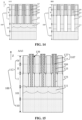
- FIG. 1 to FIG. 17 show schematic diagrams of a semiconductor structure corresponding to various operations of a method for manufacturing a semiconductor structure provided by the embodiments of the application.
- metal elements will be doped only at an end of the semiconductor channel by using relevant technical means, so as to reduce the resistivity of the end of the semiconductor channel and realize the ohmic contact between the end of the semiconductor channel and other conductive structures.
- the metal elements in the semiconductor channels will diffuse into the insulating layer, which reduces the insulating effect of the insulating layer, and increases the parasitic capacitance between adjacent semiconductor channels, thereby reducing the electrical performance of the semiconductor structure.
- the embodiments of the application provide a semiconductor structure and a method for manufacturing the semiconductor structure.
- the top surface of the semiconductor channel is provided with a metal semiconductor compound layer serving as a transition layer to realize the ohmic contact between the top surface of the semiconductor channel and other conductive structures, and to reduce the contact resistance between the top surface of the semiconductor channel and other conductive structures.
- a diffusion barrier layer is arranged between the metal semiconductor compound layer and the insulating layer to block the metal semiconductor compound layer from the insulating layer, which is beneficial to prevent metal elements in the metal semiconductor compound layer from diffusing into the insulating layer. Therefore, the embodiments of the application are beneficial to ensure good insulating performance of the insulating layer while reducing the contact resistance between the top surface of the semiconductor channel and other conductive structures through the metal semiconductor compound layer, so as to improve the electrical performance of the semiconductor structure.
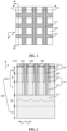
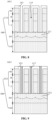
- FIG. 1 to FIG. 3 are diagrams of the semiconductor structure provided by the embodiments of the application.
- FIG. 1 is a top view of the semiconductor structure provided by the embodiments of the application.
- FIG. 2 is a schematic cross-sectional view of the semiconductor structure shown in FIG. 1 taken along a first cross-sectional direction AA1.
- FIG. 3 is a schematic cross-sectional view of the semiconductor structure shown in FIG. 1 taken along a second cross-sectional direction BB1.
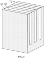
- FIG. 4 is a schematic cross-sectional view of a gate electrode surrounding a semiconductor channel and a diffusion barrier layer surrounding a metal semiconductor compound layer in the semiconductor structure.
- the semiconductor structure includes a base 100, dielectric layers 103, gate electrodes 104, metal semiconductor compound layers 105, diffusion barrier layers 106 and insulating layers 107.
- the base 100 includes bit lines 101 arranged at intervals and semiconductor channels 102 arranged at intervals.
- the bit lines 101 extend in a first direction.
- the semiconductor channels 102 are located at part of top surfaces of the bit lines 101.
- Each semiconductor channel 102 includes a first area I, a second area II, and a third area III arranged successively in a direction Z perpendicular to the top surfaces of the bit lines 101.
- the dielectric layers 103 are located between adjacent bit lines 101 and located on side walls of the semiconductor channels 102.
- the gate electrodes 104 surround the dielectric layers 103 in the second area II and extend in a second direction Y, in which the first direction X is different from the second direction Y.
- the metal semiconductor compound layers 105 are located on top surfaces of the semiconductor channels 102.
- the diffusion barrier layers 106 at least surround side walls of the metal semiconductor compound layers 105.
- the insulating layers 107 are located between the adjacent semiconductor channels 102 on the same bit line 101 and isolate the gate electrodes 104 and the diffusion barrier layers 106 located on each dielectric layer 103 from the gate electrodes 104 and the diffusion barrier layers 106 located on the dielectric layers 103 adjacent to each dielectric layer 103.
- the semiconductor channel 102, the dielectric layer 103 surrounding the side wall of the semiconductor channel 102 in the second area II, and the gate electrode 104 form a vertical GAA transistor.
- the base 100 includes a substrate 110.
- the bit line 101 is located between the substrate 110 and the GAA transistor, so that a 3D stacked semiconductor structure can be formed, which is beneficial to improve the integration density of the semiconductor structure.
- both the first area I and the third area II can serve as a source electrode or a drain electrode of the GAA transistor.
- the second area II corresponds to the dielectric layer 103 and the gate electrode 104 of the GAA transistor.
- the first direction X is perpendicular to the second direction Y, so that the semiconductor channel 102 is in an arrangement mode of 4F2 (F is the minimum pattern dimension that can be obtained under given process conditions), which is beneficial to improve the integration density of the semiconductor structure.
- the first direction intersects with the second direction, and an angle between the first direction and the second direction may not be 90°.
- bit lines 101 there are a plurality of bit lines 101 that are arranged at intervals in the base 100. Each bit line 101 may be in contact with at least one first area I. In an example shown in FIG. 1 , four bit lines 101 are arranged at intervals and each bit line 101 is in contact with four first areas I. In actual application, the number of the bit lines 101 and the number of the first areas I in contact with each bit line 101 may be reasonably set according to the actual electrical requirements.
- the semiconductor structure will be described in more detail below in combination with FIG. 1 to FIG. 3 .
- the type of the material of the base 100 may be an element semiconductor material or a crystalline inorganic compound semiconductor material.
- the element semiconductor material may be silicon or germanium.
- the crystalline inorganic compound semiconductor material may be silicon carbide, germanium silicon, gallium arsenide, indium gallium, or the like.
- the base 100 includes bit lines 101 and semiconductor channels 102.
- the base 100, the bit lines 101, and the semiconductor channels 102 have the same semiconductor element.
- the semiconductor channels 102 and the bit lines 101 may be formed by using the same film structure.
- the film structure consists of a semiconductor element, so that the semiconductor channels 102 are integrated with the bit lines 101, thereby overcoming an interface state defect between the semiconductor channels 102 and the bit lines 101, and improving the electrical performance of the semiconductor structure.
- the semiconductor element may include at least one of silicon, carbon, germanium, arsenic, gallium or indium, which will be illustrated by an example that both the bit lines 101 and the semiconductor channels 102 include silicon.
- the semiconductor structure may further include a metal silicide structure 111, and the metal silicide structure 111 is at least located in the bit lines 101 directly facing bottom surfaces of the insulating layers 107. That is, the metal silicide structure 111 is at least located in the bit lines 101 directly facing a bottom surface of the first insulating layer 117.
- the metal silicide structure 111 has relatively low resistivity compared with an unmetallized semiconductor material, thus the resistivity of the bit line 101 including the metal silicide structure 111 is lower compared with the semiconductor channel 102, which is beneficial to reduce the resistance of the bit line 101, reduce the contact resistance between the bit line 101 and the semiconductor channel 102 in the first area I, and further improve the electrical performance of the semiconductor structure.
- the resistivity of the bit line 101 is also lower than the resistivity of the substrate 110.
- the material of the areas of the bit lines 101 located directly below the first area I may be a semiconductor material, and the material of part areas of the bit lines 101 not covered by the first area I is a metal suicide. It can be understood that with the continuous reduction of the device dimension or the adjustment of manufacturing process parameters, the material of part areas of the bit lines 101 located directly below the first area I is a semiconductor material, and the material of other areas of the bit lines 101 located directly below the first area I may also be metal silicide.
- the "other areas” here are located at the periphery of "part areas”.
- a plurality of metal silicide structures 111 in the bit line 101 are communicated with each other to form part of the bit line 101, and a part of the metal silicide structure 111 may be located in the bit line 101, and another part of the metal silicide structure 111 may be located in the semiconductor channel 102 in the first area I.
- the plurality of metal silicon compound structures in the same bit line may be spaced from each other.
- the area of the base 100 defined by a dotted box similar to an ellipse is the metal silicide structure 111.
- the size of the contact area between adjacent metal silicide structures 111 is not limited.
- the bit line may include the metal silicide structure 111 in full thickness of the bit line.
- the depth of the metal silicide structure 111 gradually increases in the direction from the semiconductor channels 102 located on both sides of the insulating layer 107 to the insulating layer 107, that is, in the directions C1 and C2.
- the material of the metal silicide structure 111 includes at least one of cobalt silicide, nickel silicide, molybdenum silicide, titanium silicide, tungsten silicide, tantalum silicide, or platinum silicide.
- the semiconductor channel 102 may have a doping element, which is beneficial to improve the electrical conductivity of the semiconductor channel 102, thereby reducing the break-over voltage between the first area I and the third area III, that is, the break-over voltage between a source electrode and a drain electrode of the GAA transistor.
- the doping element is a P-type doping element or an N-type doping element.
- the N-type doping element may be at least one of arsenic, phosphorus, or antimony.
- the P-type doping element may be at least one of boron, indium, or gallium.
- the GAA transistor may be a junction-free transistor, that is, the types of the doping elements in the first area I, the second area II, and the third area II are the same.
- "Junction-free" refers to that there is no PN junction, that is, the doping concentration of the doping elements in the first area I, the second area II and the third area III is the same. This provides the following advantages. On one hand, there is no need to subjecting the first area I and the third area III with additional doping, so as to avoid the problem that it is difficult to control a doping process of the first area I and the third area III.
- the device is a junction-free transistor, which is beneficial to avoid a phenomenon of using an ultra-steep source-drain concentration gradient doping process to manufacture an ultra-steep PN junction in a nano-scale range. Therefore, this can avoid the problems such as threshold voltage drift, leakage current increase, and the like caused by doping mutation, is also beneficial to inhibit a short channel effect, and thus is helpful to further improve the integration density and the electrical performance of the semiconductor structure.
- the additional doping herein refers to a doping which is performed in such a manner that the types of the doping elements of the first area I and the third area III are different from the types of the doping elements of the second area II.
- the cross-sectional area of the semiconductor channel 102 in the first area I is greater than the cross-sectional area of the semiconductor channel 102 in the second area II.
- the cross-sectional area of the semiconductor channel 102 in the second area II is smaller than the cross-sectional area of the semiconductor channel 102 in the first area I.
- the semiconductor channel 102 in the second area II may serve as a channel area of the GAA transistor, which is beneficial to form a channel area with smaller cross-sectional area, is beneficial to improve the control capability of the gate electrode 104 surrounding the side wall of the channel area to the channel area, thereby making it easier to control the turn on or turn off of the GAA transistor.
- each dielectric layer 103 may include a first dielectric layer 113, a second dielectric layer 123 and a third dielectric layer 133.
- the first dielectric layer 113 is located between the adjacent bit lines 101, and located between the semiconductor channels 102 in the first area I on the adjacent bit lines 101.
- the second dielectric layer 123 is located on the side walls of the semiconductor channels 102 in the first area I and on a side wall of the first dielectric layer 113 in the first area I.
- the third dielectric layer 133 surrounds the side walls of the semiconductor channels 102 in the second area II and the third area III.
- the first dielectric layer 113 located between the adjacent bit lines 101 is configured to realize electrical insulation between the adjacent bit lines 101.
- the first dielectric layer 113, the second dielectric layer 123, and the insulating layer 107 located between the semiconductor channels 102 in the first areas I on the adjacent bit lines 101 work together to realize the electrical insulation between the semiconductor channels 102 in the first areas I spaced apart from each other in the first direction X and/or in the second direction Y.
- the third dielectric layer 133 surrounding the side wall of the semiconductor channel 102 in the second area II may serve as a gate dielectric layer between the subsequently formed gate electrode 104 and the semiconductor channel 102 in the second area II.
- the third dielectric layer 133 surrounding the side wall of the semiconductor channel 102 in the third area III and the insulating layer 107 work together to realize the electrical insulation between the semiconductor channels 102 in the third areas III spaced apart from each other in the first direction X and/or in the second direction Y.
- the third dielectric layer 133 may also be located on part of the side wall of the second dielectric layer 123, which is beneficial to further ensure the insulation between the gate electrode 104 and the semiconductor channel 102.
- the material of the first dielectric layer 113 is the same as the material of the second dielectric layer 123. Further, both the material of the first dielectric layer 113 and the material of the second dielectric layer 123 may be silicon oxide. In other embodiments, the material of the third dielectric layer 133, the material of the second dielectric layer 123, and the material of the first dielectric layer 113 may be the same. In yet other embodiments, the material of the third dielectric layer 133 may be different from the material of the second dielectric layer 123 and the material of the first dielectric layer 113.
- the material of the third dielectric layer 133, the material of the second dielectric layer 123 and the material of the first dielectric layer 113 only need to satisfy that the material of the third dielectric layer 133, the material of the second dielectric layer 123 and the material of the first dielectric layer 113 are materials with a good insulation effect.
- a single gate electrode 104 extends in the second direction Y, and surrounds the adjacent semiconductor channels 102 on the adjacent bit lines 101, and a single diffusion barrier layer 106 only surrounds a single metal semiconductor compound layer 105.
- an orthographic projection of the third dielectric layer 133 on the substrate 110 may overlap with an orthographic projection of the diffusion barrier layer 106 on the substrate 110.
- a single gate electrode 104 may surround a plurality of semiconductor channels 102.
- the third dielectric layer 133 is arranged between the gate electrode 104 and each of the plurality of semiconductor channels 102.
- Adjacent diffusion barrier layers 106 may be spaced apart by a second insulating layer 127.
- the material of the gate electrode 104 includes at least one of polysilicon, titanium nitride, tantalum nitride, copper or tungsten, and the material of the diffusion barrier layer 106 may be titanium nitride.
- the cross-sectional area of the semiconductor channel 102 in the first area I is greater than the cross-sectional area of the semiconductor channel 102 in the second area II.
- the dielectric layer 103 includes the first dielectric layer 113, the second dielectric layer 123, and the third dielectric layer 133. Therefore, the gate electrode 104 is at least located on part of the top surface of the first dielectric layer 113 and part of the top surface of the second dielectric layer 123, and the diffusion barrier layer 106 is located on the top surface of the third dielectric layer 133.
- the diffusion barrier layer 106 surrounds the side wall of the metal semiconductor compound layer 105, which is beneficial to prevent metal elements in the metal semiconductor compound layer 105 from diffusing into the insulating layer 107, so as to ensure good insulating performance of the insulating layer 107.
- the diffusion barrier layer 106 is located at the top surface of the third dielectric layer 133, which can also prevent relevant conductive elements in other conductive structures located on the top surface of the diffusion barrier layer 106 from diffusing into the third dielectric layer 133, to ensure good insulating performance of the third dielectric layer 133.
- an orthographic projection of the diffusion barrier layer 106 on the substrate 110 may cover an orthographic projection of the third dielectric layer 133 on the substrate 110, which is beneficial to more comprehensively prevent relevant conductive elements in other conductive structures on the top surface of the diffusion barrier layer 106 from diffusing into the third dielectric layer 133.
- the dielectric layer includes a first dielectric layer, a second dielectric layer, and a third dielectric layer, and in a plane perpendicular to the side wall of the semiconductor channel, the cross-sectional area of the semiconductor channel in the first area is equal to the cross-sectional area of the semiconductor channel in the second area, then the third dielectric layer and the gate electrode cover the top surface of the second dielectric layer together.
- the metal semiconductor compound layer 105 has relatively low resistivity compared with an unmetallized semiconductor material, thus the metal semiconductor compound layer 105 has lower resistivity compared with the semiconductor channel 102. If an electrical connection layer 108 is arranged on the top surface of each metal semiconductor compound layer 105, the metal semiconductor compound layer 105 may be used as the transition layer to form ohmic contact between the top surface of the semiconductor channel 102 and the electrical connection layer 108, and the electrical connection layer 108 is prevented from being in direct contact with the semiconductor material to form Schottky barrier contact.
- the ohmic contact is beneficial to reduce the contact resistance between the top surface of the semiconductor channel 102 and the electrical connection layer 108, so as to reduce the energy consumption of the semiconductor structure during working, improve a Resistance-Capacitance (RC) delay effect, and improve the electrical performance of the semiconductor structure.
- the material of the metal semiconductor compound layer 105 includes at least one of cobalt silicide, nickel silicide, molybdenum silicide, titanium silicide, tungsten silicide, tantalum silicide, or platinum silicide.
- the metal semiconductor compound layer 105 may have a doping element, and the doping element is a P-type doping element or an N-type doping element. Thus, this is beneficial to further improve the electrical conductivity of the metal semiconductor compound layer 105.
- the semiconductor channel 102 may have the doping element with the same type as the doping element of the metal semiconductor compound layer 105, and the concentration of the doping element in the metal semiconductor compound layer 105 is greater than the concentration of the doping element in the semiconductor channel 102.
- this is beneficial to further reduce the contact resistance between the metal semiconductor compound layer 105 and the semiconductor channel 102 while improving the electrical conductivity of the semiconductor channel 102.
- the top surfaces of the metal semiconductor compound layers 105 may be flush with the top surfaces of the diffusion barrier layers 106.
- the length of the metal semiconductor compound layer 105 is less than or equal the length of the diffusion barrier layer 106.
- the diffusion barrier layer 106 may at least surround a side wall of the entire metal semiconductor compound layer 105, and increase the total area over which the diffusion barrier layer 106 functions to prevent diffusion, so as to improve the effect of preventing the metal elements in the metal semiconductor compound layer 105 from diffusing into the insulating layer 107.
- the length of the diffusion barrier layer 106 is greater than the length of the metal semiconductor compound layer 105, that is, the diffusion barrier layer 106 further surrounds the side wall of part of the semiconductor channel 102, which is beneficial to improve the doping element in the semiconductor channel 102 from diffusing into the insulating layer 107.
- the ratio of the length of the metal semiconductor compound layer 105 to the length of the diffusion barrier layer 106 may be 0.8 to 1.2. Thus, this is beneficial to ensure that there is an appropriate spacing between the diffusion barrier layer 106 and the gate electrode 104 and avoid parasitic capacitance between the diffusion barrier layer 106 and the gate electrode 104.
- each insulating layer 107 includes a first insulating layer 117 and a second insulating layer 127.
- the first insulating layer 117 is located between the dielectric layers 103 of the adjacent semiconductor channels 102 and between the gate electrodes 104, and extends in the second direction Y, and the top surface of the first insulating layer 117 is not lower than the top surface of the metal semiconductor compound layer 105.
- the second insulating layer 127 is located at the top surface of a respective one of the gate electrodes 104, and located between the first insulating layer 117 and a respective one of the diffusion barrier layers 106.
- the first insulating layer 117 and the second insulating layer 127 work together to realize the electrical insulation between the adjacent semiconductor channels 102 and the electrical insulation between the adjacent gate electrodes 104.
- the second insulating layer 127 located at the top surface of the gate electrode 104 may realize the electrical insulation between the gate electrode 104 and other conductive structures.
- the semiconductor structure may further include electrical connection layers 108 located at the top surfaces of the metal semiconductor compound layers 105 and the top surfaces of the diffusion barrier layers 106.
- the insulating layers 107 isolate the adjacent electrical connection layers 108 at the top surfaces of the adjacent semiconductor channels 102 from each other.
- the electrical connection layer 108 may be configured to realize electrical connection between the semiconductor channel 102 and a capacitor structure (not shown in the figures).
- the metal semiconductor compound layer 105 has relatively low resistivity compared with an unmetallized semiconductor channel 102, which is beneficial to realize ohmic contact between the top surface of the semiconductor channel 102 and other conductive structures, such as the electrical connection layer 108, through the metal semiconductor compound layer 105, and reduce the contact resistance between the top surface of the semiconductor channel 102 and the electrical connection layer 108, so as to improve the electrical performance of the semiconductor channel 102.
- the metal semiconductor compound layer 105 is blocked from the insulating layer 107 by the diffusion barrier layer 106, which is beneficial to prevent metal elements in the metal semiconductor compound layer 105 from diffusing into the insulating layer 107 which may result in the reduction of the insulating performance of the insulating layer 107.
- the embodiments of the application are beneficial to ensure good insulating performance of the insulating layer 107 while reducing the contact resistance between the top surface of the semiconductor channel 102 and the electrical connection layer 108 through the metal semiconductor compound layer 105, so as to improve the electrical performance of the semiconductor structure.
- Another embodiment of the application further provides a method for manufacturing a semiconductor structure, which can be used to form the semiconductor structure mentioned above.
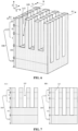
- FIG. 1 to FIG. 17 are schematic cross-sectional views of a semiconductor structure corresponding to various operations of a method for manufacturing a semiconductor structure provided by the embodiments of the application.
- the method for manufacturing the semiconductor structure provided by the embodiments of the application will be described in detail below in combination with the accompanying drawings. The parts that are the same as or correspond to the embodiments mentioned above will not be elaborated in detail below.
- FIG. 1 to FIG. 17 in the present embodiment are partial schematic diagrams of the semiconductor structure.
- FIG. 7 shows schematic cross-sectional views of a structure as shown in FIG. 6 taken along a first cross-sectional direction AA1 and a second cross-sectional direction BB1. It is to be noted that one or two of the schematic cross-sectional views taken along the first cross-sectional direction AA1 and the second cross-sectional direction BB1 will be set according to the requirement of statement subsequently.
- the base 100 includes bit lines 101 arranged at intervals and initial semiconductor channels 112 arranged at intervals.
- the bit lines 101 extend in a first direction X.
- the initial semiconductor channels 102 are located at part of top surfaces of the bit lines 101.
- Each initial semiconductor channel 112 includes a first area I, a second area II, and an initial third area IV arranged successively in a direction Z perpendicular to the top surfaces of the bit lines 101.
- the dielectric layers 103 are formed. The dielectric layers 103 are located between adjacent bit lines 101 and located on part of the side walls of the initial semiconductor channels 112.
- first area I and the second area II of the initial semiconductor channel 112 are a first area and a second area of subsequent semiconductor channel.
- the initial third area IV of the initial semiconductor channel 112 prepares for the subsequent formation of a third area of the semiconductor channel and a metal semiconductor compound layer.
- both the first area I and the subsequently formed third area II may serve as a source electrode or a drain electrode of the subsequently formed GAA transistor with the semiconductor channel, and the second area II corresponds to the dielectric layer and the gate electrode of the subsequently formed GAA transistor.
- the operation that the base 100 is provided may include the following operations.
- an initial base 120 is provided.
- Initial first dielectric layers 143 extending in the first direction X are arranged in the initial base 120.
- the initial base 120 and the initial first dielectric layers 143 are patterned, to form the bit lines 101 arranged at intervals and the initial semiconductor channels 112 arranged at intervals, and the initial first dielectric layers 143 located between the adjacent bit lines 101.
- the top surfaces of the initial first dielectric layers 143 are not lower than the top surfaces of the initial semiconductor channels 112.
- the side walls of the initial semiconductor channels 112, the side walls of the initial first dielectric layers 143, and part of the top surfaces of the bit lines 101 define grooves 109.
- the grooves 109 extend in the second direction Y.
- the type of the material of the initial base 120 may be an element semiconductor material or a crystalline inorganic compound semiconductor material.
- the element semiconductor material may be silicon or germanium.
- the crystalline inorganic compound semiconductor material may be silicon carbide, germanium silicon, gallium arsenide, indium gallium, or the like.
- the initial base 120 is the basis for forming the bit line 101 and the initial semiconductor channel 112.
- a substrate 110 is also formed while patterning the initial base 120 and the initial first dielectric layer 143 to form the bit line 101 and the initial semiconductor channel 112.
- a method for patterning the initial base 120 and the initial first dielectric layer 143 includes Self-Aligned Quadruple Patterning, SAQP, or Self-aligned Double Patterning, SADP.
- the initial base 120 may also be doped and annealed, so that an N-type doping element or a P-type doping element is doped in the initial base 120, which is beneficial to improve the electrical conductivity of the initial semiconductor channel 102 formed by taking the initial base 120 as the basis, thereby reducing the break-over voltage between the first area I and the initial third area III, that is, reducing the break-over voltage between a source electrode and a drain electrode in the subsequently formed GAA transistor.
- the N-type doping element or the P-type doping element is doped in the initial base 120, which is beneficial to improve the electrical conductivity of the bit line 101 formed by taking the initial base 120 as the basis, thereby reducing the contact resistance between the first area I and the bit line 101, and improving the electrical performance of the semiconductor structure.
- the doping element is a P-type doping element or an N-type doping element.
- the N-type doping element may be at least one of arsenic, phosphorus, or antimony.
- the P-type doping element may be at least one of boron, indium, or gallium.
- gate electrodes 104 are formed.
- the gate electrodes 104 surround the dielectric layers 103 in the second area II and extend in the second direction Y, and the first direction X is different from the second direction Y.
- the diffusion barrier layers 106 are formed.
- the diffusion barrier layers 106 surround the remaining portion of the side walls of the initial semiconductor channels 112, and there is a spacing between each of the diffusion barrier layers 106 and a respective one of the gate electrodes 104.
- the metal siliconizing treatment is performed on top surfaces of the initial semiconductor channels 112 to transform part of the initial semiconductor channels 112 in the initial third area IV into metal semiconductor compound layers 105, in which the remaining portion of the initial third area IV, the second area II, and the third area III form the semiconductor channels 102.
- the insulating layers 107 are formed. The insulating layers 107 are located between adjacent semiconductor channels 102 on the same bit line 101.
- the operation that the metal semiconductor compound layer 105 is formed through the metal siliconizing treatment may include the following operation.
- a first metal layer (not shown in the figures) is formed on the top surface of the initial semiconductor channel 112, in which the first metal layer provides metal elements for the metal semiconductor compound layer 105.
- the material of the first metal layer includes at least one of cobalt, nickel, molybdenum, titanium, tungsten, tantalum, or platinum.
- the operation that the dielectric layer 103, the gate electrode 104, the diffusion barrier layer 106, and the insulating layer 107 are formed may include the following operations.
- a first dielectric layer 113 is formed between the adjacent bit lines 101 and between the semiconductor channels 102 in the first area I on the adjacent bit lines 101.
- a second dielectric layer 123 is formed on side walls of the grooves 109 in the first area I.
- a first insulating layer 117 is formed. The first insulating layer 117 is located in the groove 109 and isolates the adjacent second dielectric layers 123 from each other. The top surface of the first insulating layer 117 is not lower than the top surface of the initial semiconductor channel 112.
- the top surface of the first insulating layer 117 is not lower than the top surface of the initial semiconductor channel 112, which is beneficial to form a second spacing between the first insulating layer 117 and the semiconductor channels 102 in the second area II and the third area III. Then, a gate electrode with an accurate dimension may be formed in the second spacing in a self-aligned manner.
- the gate electrode with high dimension accuracy can be formed without an etching process, which is beneficial to simplify the operation of forming the gate electrode, and a small-dimension gate electrode can be obtained by regulating and controlling the dimension of the second spacing.
- the operation that the first dielectric layer 113, the second dielectric layer 123, and the first insulating layer 117 are formed may include the following operations.
- initial second dielectric layers 153 are formed on the side walls of the grooves 109 (with reference to FIG. 7 ), and there is a first spacing 119 between adjacent initial second dielectric layers 153.
- the initial second dielectric layers 153 may be formed by using the following process operation. A deposition process is performed to form a surface that covers the top surfaces and all the exposed side walls of the semiconductor channels 102, and covers the exposed top surfaces and the side walls of the initial first dielectric layers 143.
- the material of the initial second dielectric layer 153 includes silicon oxide.
- the first insulating layer 117 is formed in the first spacing 119.
- the first insulating layer 117 may be formed by using the following process operations. A first insulating film that covers the top surface of the initial second dielectric layer 153 and fills the first spacing 119 is formed. The chemical mechanical flattening treatment is performed on the first insulating film until the initial second dielectric layer 153 is exposed, in which the remaining portion of the first insulating film forms the first insulating layer 117.
- the material of the first insulating layer 117 includes silicon nitride.
- the material of the initial first dielectric layer 143 and the material of the initial second dielectric layer 153 are the same, which is beneficial to remove part of the initial first dielectric layer 143 and part of the initial second dielectric layer 153 through the same removal operation, so as to form a second spacing.
- the metal siliconizing treatment is performed on part of the top surface of the bit line 101 exposed by the initial second dielectric layer 153 to form a metal silicide structure 111before the first insulating layer 117 is formed and after the initial second dielectric layer 153 is formed.
- the metal silicide structure 111 has relatively low resistivity compared with an unmetallized semiconductor material, thus the resistivity of the bit line 101 including the metal silicide structure 111 is lower compared with the semiconductor channel 102, which is beneficial to reduce the resistance of the bit line 101, reduce the contact resistance between the bit line 101 and the semiconductor channel 102 in the first area I, and further improve the electrical performance of the semiconductor structure.
- the operation that the metal siliconizing treatment is performed on part of the top surface of the bit line 101 exposed by the initial second dielectric layer 153 may include the following operation.
- a second metal layer (not shown in the figures) is formed on the exposed top surface of the bit line 101, in which the second metal layer provides metal elements for the metal silicide structure 111.
- the material of the second metal layer includes at least one of cobalt, nickel, molybdenum, titanium, tungsten, tantalum or platinum.
- the metal siliconizing treatment may also not be performed on the exposed top surface of the bit line, and the first insulating layer may be directly formed on the exposed top surface of the bit line.
- the initial first dielectric layer 143 and the initial second dielectric layer 153 are etched by taking the first insulating layer 117 as a mask, to form the first dielectric layer 113 and the second dielectric layer 123.
- the top surface of the semiconductor channel 102 is further exposed, which facilitates subsequent metal siliconizing treatment on the top surface of the semiconductor channel 102 to form the metal semiconductor compound layer.
- a third dielectric layer 133 and a second insulating layer 127 are formed.
- the third dielectric layer 133 is located on the side walls of the grooves 109 in the second area II and part of the side walls of the grooves 109 in the initial third area IV.
- the second insulating layer 127 is located between the first insulating layer 117 and the third dielectric layer 133.
- the diffusion barrier layers 106 are formed in the remaining portion of the side walls of the grooves 109 in the initial third area IV.
- the first dielectric layer 113, the second dielectric layer 123, and the third dielectric layer 133 form the dielectric layers 103.
- the first insulating layer 117 and the second insulating layer 127 form insulating layers 107.
- the operation that the third dielectric layer 133, the gate electrode 104, and second insulating layer 127 are formed may include the following operations.
- an initial third dielectric layer 163 is formed on the side walls of the initial semiconductor channels 112 in the second area II and the initial third area IV, and there is a second spacing 129 between the initial third dielectric layer 163 and the first insulating layer 117.
- the initial third dielectric layer 163 may be formed by using the following process operations. The thermal oxidation treatment is performed on the exposed surfaces of the initial semiconductor channels 112 in the second area II and the initial third area IV, to form an initial third dielectric layer 163.
- the material of the initial third dielectric layer 163 is silicon oxide.
- the initial third dielectric layer that covers the surfaces of the initial semiconductor channels in the second area and the initial third area may also be formed through a deposition process.
- the gate electrode 104 is formed in the second spacing 129 (with reference to FIG. 11 ) in the second area II.
- the operation that the gate electrode 104 is formed may include the following operations.
- an initial gate electrode 114 is formed, in which the initial gate electrode 114 fills the second spacing 129 and is located on the top surface of the initial third dielectric layer 163.
- the initial gate electrode 114 which surrounds the side wall of the semiconductor channel 102 in the initial third area IV and which is located on the top surface of the initial third dielectric layer 163 is removed by etching, in which the remaining portion of the initial gate electrode 114 forms the gate electrode 104, and the gate electrode 104 only surrounds the side wall of the semiconductor channel 102 in the second area II.
- the second insulating layer 127 is formed in the remaining portion of the second spacing 129.
- the second insulating layer 127 may be formed by using the following process operations.
- a deposition process is performed to form a second insulating film that fills the remaining portion of the second spacing 129 (with reference to FIG. 11 ) and covers the top surface of the initial third dielectric layer 163.
- the chemical mechanical grinding is performed on the second insulating film and the first insulating layer 117 until the initial third dielectric layer 163 is exposed, in which the remaining portion of the second insulating film forms the second insulating layer 127.
- the material of the second insulating film includes silicon nitride.
- the initial third dielectric layer 163 is etched by taking the second insulating layer 127 as a mask, to form the third dielectric layer 133.
- the third dielectric layer 133 In the operation that the third dielectric layer 133 is formed, not only the top surface of the initial semiconductor channel 112 is exposed, but also part of the side wall, close to the top surface, of the initial semiconductor channel 112 in the initial third area IV is also exposed, which prepares for subsequent formation of the diffusion barrier layer.
- the third dielectric layer 133, the second insulating layer 127, and the initial semiconductor channel 112 define grooves 139, and diffusion barrier layers 106 filling the grooves 139 are formed.
- the diffusion barrier layer 106 may be formed by using the following process operations. A barrier film that covers the top surface of the initial semiconductor channel 112 and fills the groove 139 is formed. The barrier film is etched until part of a side wall, close to the top surface, of the initial semiconductor channel 112 in the initial third area IV is exposed, in which the remaining portion of the barrier film forms the diffusion barrier layer 106.
- the material of the diffusion barrier layer 106 includes titanium nitride.
- the diffusion barrier layer 106 is beneficial to prevent metal elements in the metal semiconductor compound layer 105 from diffusing into the insulating layer 107, to ensure good insulating performance of the insulating layer 107.
- the diffusion barrier layer 106 is located at the top surface of the third dielectric layer 133, which can also prevent relevant conductive elements in other conductive structures located on the top surface of the diffusion barrier layer 106 from diffusing into the third dielectric layer 133, to ensure good insulating performance of the third dielectric layer 133.
- the metal siliconizing treatment is performed on the top surfaces of the initial semiconductor channels 112, to transform part of the initial semiconductor channels 112 in the initial third area IV into the metal semiconductor compound layers 105.
- the remaining portion of the initial third area IV, the second area II, and the third area III form the semiconductor channels 102.
- the metal semiconductor compound layer 105 has lower resistivity compared with the semiconductor channel 102.
- An electrical connection layer is formed on the top surface of the metal semiconductor compound layer 105, which is beneficial to take the metal semiconductor compound layer 105 as a transition layer to form ohmic contact between the top surface of the semiconductor channel 102 and the electrical connection layer, and prevent the electrical connection layer from being in direct contact with the semiconductor channel 102 to form Schottky barrier contact.
- the ohmic contact is beneficial to reduce the contact resistance between the top surface of the semiconductor channel 102 and the electrical connection layer, reduce the energy consumption of the semiconductor structure during working, improve the RC delay effect, and improve the electrical performance of the semiconductor structure.
- the method may further includes the following operation.
- the top surface of the initial semiconductor channel 112 is doped, so that part of the initial semiconductor channels 112 in the initial third area IV has a doping element, in which the doping element is a P-type doping element or an N-type doping element.
- the semiconductor channel 102 may have the doping element with the same type as the doping element in the metal semiconductor compound layer 105, and the concentration of the doping element in the metal semiconductor compound layer 105 is greater than the concentration of the doping element in the semiconductor channel 102.
- this is beneficial to further reduce the contact resistance between the metal semiconductor compound layer 105 and the semiconductor channel 102 while improving the electrical conductivity of the semiconductor channel 102.
- the top surface of the insulating layer 107 is higher than the top surface of the metal semiconductor compound layer 105.
- the insulating layer 107, the metal semiconductor compound layer 105, and the diffusion barrier layer 106 define a through hole 149.
- the method may further include the following operation.
- An electrical connection layer 108 that fills the through hole 149 is formed.
- the electrical connection layer 108 may be configured to realize electrical connection between the semiconductor channel 102 and a capacitor structure (not shown in the figures).
- a second spacing 129 is formed between the first insulating layer 117 and the semiconductor channels 102 in the second area II and the third area III, which is beneficial to form a gate electrode 104 with an accurate dimension in the second spacing 129 in a self-aligned manner.
- the gate electrode 104 with high dimension accuracy can be formed without an etching process, which is beneficial to simplify the operation of forming the gate electrode 104, and a small-dimension gate electrode 104 can be obtained by regulating and controlling the dimension of the second spacing 129.
- the metal semiconductor compound layer 105 serving as a transition layer is formed on the top surface of the semiconductor channel 102, to realize ohmic contact between the top surface of the semiconductor channel 102 and the electrical connection layer 108, and reduce the contact resistance between the top surface of the semiconductor channel 102 and the electrical connection layer 108.
- the diffusion barrier layer 106 is formed between the metal semiconductor compound layer 105 and the insulating layer 107 to block the metal semiconductor compound layer 105 from the insulating layer 107, which is beneficial to prevent the metal elements in the metal semiconductor compound layer 105 from diffusing into the insulating layer 107, thereby ensuring good insulating performance of the insulating layer 107 while reducing the contact resistance between the top surface of the semiconductor channel 102 and the electrical connection layer 108 through the metal semiconductor compound layer 105, and improving the electrical performance of the semiconductor structure.
- the embodiments of the application provide a semiconductor structure and a method for manufacturing the semiconductor structure.
- the semiconductor structure includes a base, dielectric layers, gate electrodes, metal semiconductor compound layers, diffusion barrier layers and insulating layers.
- the base includes bit lines arranged at intervals and semiconductor channels arranged at intervals. The bit lines extend in a first direction.
- the semiconductor channels are located at part of top surfaces of the bit lines. Each semiconductor channel includes a first area, a second area, and a third area arranged successively in a direction perpendicular to the top surfaces of the bit lines.
- the dielectric layers are located between adjacent bit lines and located on side walls of the semiconductor channels.
- the gate electrodes surround the dielectric layer in the second area and extend in a second direction, in which the first direction is different from the second direction.
- the metal semiconductor compound layers are located on top surfaces of the semiconductor channels.
- the diffusion barrier layers at least surround side walls of the metal semiconductor compound layers.
- the insulating layers are located between the adjacent semiconductor channels on the same bit line and isolate the gate electrodes and the diffusion barrier layers located on each dielectric layer from the gate electrodes and the diffusion barrier layers located on the dielectric layers adjacent to each dielectric layer.
- a vertical GAA transistor is formed in the base, and the bit lines are buried in the base and are located below the semiconductor channels, so that a Three-Dimensional, 3D, stacked semiconductor structure can be formed, which is beneficial to improve the integration density of the semiconductor structure.
- metal semiconductor compound layers are provided on the top surfaces of the semiconductor channels far away from the bit lines. Since the metal semiconductor compound layer has relatively low resistivity compared with an unmetallized semiconductor channel, the metal semiconductor compound layer can serve as a transition layer to realize ohmic contact between the top surface of the semiconductor channel and other conductive structures, and reduce the contact resistance between the top surface of the semiconductor channel and other conductive structures, so as to improve the electrical performance of the semiconductor channel.
- the diffusion barrier layer at least surrounds the side wall of the metal semiconductor compound layer, so that the metal semiconductor compound layer is blocked from the insulating layer by the diffusion barrier layer, which is beneficial to prevent metal elements in the metal semiconductor compound layer from diffusing into the insulating layer which may result in the reduction of the insulating performance of the insulating layer. Therefore, the embodiments of the application are beneficial to ensure good insulating performance of the insulating layer while reducing the contact resistance between the top surface of the semiconductor channel and other conductive structures through the metal semiconductor compound layer, so as to improve the electrical performance of the semiconductor structure.
Landscapes
- Engineering & Computer Science (AREA)
- Manufacturing & Machinery (AREA)
- Semiconductor Memories (AREA)
- Electrodes Of Semiconductors (AREA)
Applications Claiming Priority (2)
| Application Number | Priority Date | Filing Date | Title |
|---|---|---|---|
| CN202111243328.2A CN116033740B (zh) | 2021-10-25 | 2021-10-25 | 半导体结构及其制造方法 |
| PCT/CN2022/072992 WO2023070963A1 (fr) | 2021-10-25 | 2022-01-20 | Structure semi-conductrice et procédé de fabrication associé |
Publications (2)
| Publication Number | Publication Date |
|---|---|
| EP4199089A4 EP4199089A4 (fr) | 2023-06-21 |
| EP4199089A1 true EP4199089A1 (fr) | 2023-06-21 |
Family
ID=86055405
Family Applications (1)
| Application Number | Title | Priority Date | Filing Date |
|---|---|---|---|
| EP22715511.6A Pending EP4199089A1 (fr) | 2021-10-25 | 2022-01-20 | Structure semi-conductrice et procédé de fabrication associé |
Country Status (4)
| Country | Link |
|---|---|
| US (1) | US12336164B2 (fr) |
| EP (1) | EP4199089A1 (fr) |
| JP (1) | JP7483891B2 (fr) |
| KR (1) | KR102707225B1 (fr) |
Families Citing this family (3)
| Publication number | Priority date | Publication date | Assignee | Title |
|---|---|---|---|---|
| EP4138132A1 (fr) * | 2021-07-09 | 2023-02-22 | Changxin Memory Technologies, Inc. | Structure semi-conductrice et son procédé de fabrication |
| US12309998B2 (en) * | 2022-05-20 | 2025-05-20 | Changxin Memory Technologies, Inc. | Semiconductor structure and method for manufacturing semiconductor structure |
| CN121194461A (zh) * | 2024-06-21 | 2025-12-23 | 长鑫科技集团股份有限公司 | 半导体结构、半导体器件及半导体结构的制备方法 |
Family Cites Families (16)
| Publication number | Priority date | Publication date | Assignee | Title |
|---|---|---|---|---|
| US5770484A (en) | 1996-12-13 | 1998-06-23 | International Business Machines Corporation | Method of making silicon on insulator buried plate trench capacitor |
| KR100739532B1 (ko) * | 2006-06-09 | 2007-07-13 | 삼성전자주식회사 | 매몰 비트라인 형성 방법 |
| JP5623005B2 (ja) | 2008-02-01 | 2014-11-12 | ピーエスフォー ルクスコ エスエイアールエルPS4 Luxco S.a.r.l. | 半導体装置及びその製造方法 |
| KR101149043B1 (ko) * | 2009-10-30 | 2012-05-24 | 에스케이하이닉스 주식회사 | 매립형 비트라인을 구비하는 반도체 장치 및 그 제조방법 |
| JP2012038994A (ja) * | 2010-08-10 | 2012-02-23 | Elpida Memory Inc | 半導体装置及びその製造方法 |
| JP2013026382A (ja) * | 2011-07-20 | 2013-02-04 | Elpida Memory Inc | 半導体装置の製造方法 |
| US8395139B1 (en) | 2011-12-06 | 2013-03-12 | Nanya Technology Corp. | 1T1R resistive memory device and fabrication method thereof |
| US9023723B2 (en) * | 2012-05-31 | 2015-05-05 | Applied Materials, Inc. | Method of fabricating a gate-all-around word line for a vertical channel DRAM |
| KR20140003206A (ko) * | 2012-06-29 | 2014-01-09 | 에스케이하이닉스 주식회사 | 매립비트라인을 구비한 반도체 장치 및 그 제조방법 |
| KR102102782B1 (ko) | 2013-07-24 | 2020-04-22 | 에스케이하이닉스 주식회사 | 멀티 레이어 게이트를 갖는 반도체 장치, 이를 포함하는 전자 장치 및 그 반도체 장치의 제조 방법 |
| KR102269228B1 (ko) * | 2014-07-31 | 2021-06-25 | 삼성전자주식회사 | 반도체 장치의 제조 방법 |
| US10014305B2 (en) * | 2016-11-01 | 2018-07-03 | Micron Technology, Inc. | Methods of forming an array comprising pairs of vertically opposed capacitors and arrays comprising pairs of vertically opposed capacitors |
| US9935114B1 (en) * | 2017-01-10 | 2018-04-03 | Micron Technology, Inc. | Methods of forming an array comprising pairs of vertically opposed capacitors and arrays comprising pairs of vertically opposed capacitors |
| KR102373616B1 (ko) * | 2017-07-06 | 2022-03-11 | 삼성전자주식회사 | 반도체 장치 및 그 제조 방법 |
| CN108198815B (zh) | 2017-12-27 | 2020-12-22 | 中国科学院微电子研究所 | 半导体器件及其制造方法及包括该器件的电子设备 |
| CN113035776A (zh) | 2021-03-11 | 2021-06-25 | 长鑫存储技术有限公司 | 半导体结构及其制备方法 |
-
2022
- 2022-01-20 EP EP22715511.6A patent/EP4199089A1/fr active Pending
- 2022-01-20 KR KR1020227021222A patent/KR102707225B1/ko active Active
- 2022-01-20 JP JP2022539197A patent/JP7483891B2/ja active Active
- 2022-04-18 US US17/722,563 patent/US12336164B2/en active Active
Also Published As
| Publication number | Publication date |
|---|---|
| US20230128761A1 (en) | 2023-04-27 |
| EP4199089A4 (fr) | 2023-06-21 |
| KR102707225B1 (ko) | 2024-09-20 |
| US12336164B2 (en) | 2025-06-17 |
| KR20230062467A (ko) | 2023-05-09 |
| JP2023550855A (ja) | 2023-12-06 |
| JP7483891B2 (ja) | 2024-05-15 |
Similar Documents
| Publication | Publication Date | Title |
|---|---|---|
| EP4231342B1 (fr) | Structure semi-conductrice et son procédé de fabrication | |
| US9252239B2 (en) | Semiconductor power devices manufactured with self-aligned processes and more reliable electrical contacts | |
| US9735266B2 (en) | Self-aligned contact for trench MOSFET | |
| KR100385408B1 (ko) | 반도체 장치 및 그 제조 방법 | |
| US12336164B2 (en) | Semiconductor structure and method for manufacturing semiconductor structure | |
| US9722071B1 (en) | Trench power transistor | |
| US12309997B2 (en) | Semiconductor structure and method for fabricating same | |
| CN116033741B (zh) | 半导体结构及其制造方法 | |
| US12114485B2 (en) | Semiconductor structure and method for manufacturing same | |
| CN116033740B (zh) | 半导体结构及其制造方法 | |
| US20220278209A1 (en) | High voltage field effect transistors with metal-insulator-semiconductor contacts and method of making the same | |
| US12369295B2 (en) | Semiconductor structure and manufacturing method thereof | |
| US11996457B2 (en) | Semiconductor devices | |
| TWI823639B (zh) | 半導體裝置及其形成方法 | |
| RU2810689C1 (ru) | Полупроводниковая структура и способ ее изготовления | |
| US12408378B2 (en) | Semiconductor structure and method for manufacturing same | |
| US12414285B2 (en) | Semiconductor structure and manufacturing method thereof |
Legal Events
| Date | Code | Title | Description |
|---|---|---|---|
| STAA | Information on the status of an ep patent application or granted ep patent |
Free format text: STATUS: UNKNOWN |
|
| STAA | Information on the status of an ep patent application or granted ep patent |
Free format text: STATUS: THE INTERNATIONAL PUBLICATION HAS BEEN MADE |
|
| PUAI | Public reference made under article 153(3) epc to a published international application that has entered the european phase |
Free format text: ORIGINAL CODE: 0009012 |
|
| STAA | Information on the status of an ep patent application or granted ep patent |
Free format text: STATUS: REQUEST FOR EXAMINATION WAS MADE |
|
| 17P | Request for examination filed |
Effective date: 20220420 |
|
| A4 | Supplementary search report drawn up and despatched |
Effective date: 20230102 |
|
| AK | Designated contracting states |
Kind code of ref document: A1 Designated state(s): AL AT BE BG CH CY CZ DE DK EE ES FI FR GB GR HR HU IE IS IT LI LT LU LV MC MK MT NL NO PL PT RO RS SE SI SK SM TR |
|
| DAV | Request for validation of the european patent (deleted) | ||
| DAX | Request for extension of the european patent (deleted) |