EP4199355A1 - Agencement du circuit électronique destiné à la distribution de courant - Google Patents
Agencement du circuit électronique destiné à la distribution de courant Download PDFInfo
- Publication number
- EP4199355A1 EP4199355A1 EP21214298.8A EP21214298A EP4199355A1 EP 4199355 A1 EP4199355 A1 EP 4199355A1 EP 21214298 A EP21214298 A EP 21214298A EP 4199355 A1 EP4199355 A1 EP 4199355A1
- Authority
- EP
- European Patent Office
- Prior art keywords
- mosfet
- transistor
- circuit arrangement
- electronic circuit
- connection
- Prior art date
- Legal status (The legal status is an assumption and is not a legal conclusion. Google has not performed a legal analysis and makes no representation as to the accuracy of the status listed.)
- Granted
Links
Images



Classifications
-
- H—ELECTRICITY
- H03—ELECTRONIC CIRCUITRY
- H03K—PULSE TECHNIQUE
- H03K17/00—Electronic switching or gating, i.e. not by contact-making and –breaking
- H03K17/12—Modifications for increasing the maximum permissible switched current
- H03K17/122—Modifications for increasing the maximum permissible switched current in field-effect transistor switches
-
- H—ELECTRICITY
- H03—ELECTRONIC CIRCUITRY
- H03K—PULSE TECHNIQUE
- H03K17/00—Electronic switching or gating, i.e. not by contact-making and –breaking
- H03K17/14—Modifications for compensating variations of physical values, e.g. of temperature
- H03K17/145—Modifications for compensating variations of physical values, e.g. of temperature in field-effect transistor switches
-
- H—ELECTRICITY
- H03—ELECTRONIC CIRCUITRY
- H03K—PULSE TECHNIQUE
- H03K17/00—Electronic switching or gating, i.e. not by contact-making and –breaking
- H03K17/51—Electronic switching or gating, i.e. not by contact-making and –breaking characterised by the components used
- H03K17/56—Electronic switching or gating, i.e. not by contact-making and –breaking characterised by the components used by the use, as active elements, of semiconductor devices
- H03K17/687—Electronic switching or gating, i.e. not by contact-making and –breaking characterised by the components used by the use, as active elements, of semiconductor devices the devices being field-effect transistors
- H03K17/6877—Electronic switching or gating, i.e. not by contact-making and –breaking characterised by the components used by the use, as active elements, of semiconductor devices the devices being field-effect transistors the control circuit comprising active elements different from those used in the output circuit
Definitions
- the invention relates to an electronic circuit arrangement for power distribution.
- the invention also relates to a method for the even distribution of a current and the use of the electronic circuit arrangement in a circuit for simulating a battery.
- Fig. 1 a) and 1 b) shown basic circuits of parallel transistors T1, T2, T3, T4 known. These circuits are suitable, inter alia, for distributing the power loss of a current present at an input connection 6 downstream of an output connection 9 over a plurality of transistors T1, T2, T3, T4 connected in parallel.
- the in the 1 a) and b) Electronic circuits shown each have a terminal 10 for a control voltage.
- a parallel connection of transistors for current distribution always involves the challenge of distributing the current or power loss as evenly as possible so that individual components do not overheat.
- An electronic circuit is preferably specified in which a plurality of MOSFETs are connected in parallel in order to increase the maximum power loss with an even distribution of the current in the predominantly linear operation of the MOSFETs.
- linear operation or also as a “linear operating mode” of a MOSFET is referred to in technical circles, as also in the present context, a way of using the MOSFET, in which the MOSFET is not fully controlled by a predefined gate-source voltage, or otherwise Expressed as:
- the MOSFET In linear operation, the MOSFET has a significantly higher Nth drain-source voltage for a given drain-source current than - especially with a fully controlled MOSFET - a minimum achievable M- with the given drain-source current. te drain-source voltage.
- the technical object of the invention is achieved by an electronic circuit arrangement for evenly dividing a current, having a first MOSFET and a second MOSFET, the first MOSFET and the second MOSFET being connected in parallel in order to direct a current present at an input connection to an output connection of the circuit arrangement, the input connection being connected to the drain connection of the first MOSFET and to the drain connection of the second MOSFET, the electronic circuit arrangement comprising a connection for a control voltage, the control voltage at the gate connection of the first MOSFET and applied to the gate terminal of the second MOSFET, the first MOSFET has a first resistor at the gate terminal and the second MOSFET has a second resistor at the gate terminal, the source terminal of the first MOSFET has a first source resistor and the source terminal of the second MOSFET are connected to a second source resistor, the first source resistor and the second source resistor being connected to the output terminal of the circuit arrangement, characterized in that the circuit arrangement comprises a first transistor, the base of the first transistor having
- the basic idea of the present invention is to place a transistor in each MOSFET in such a way that the transistor is thermally coupled to the MOSFET. This achieves the technical advantage that the transistors also serve as temperature sensors and not only the current but also the temperature between the MOSFETs connected in parallel is balanced.
- the circuit can work with very small source resistances, which reduces the voltage drop when fully switched on. As a result, the maximum power loss for MOSFETs connected in parallel can be increased.
- the first transistor has a first capacitor at the collector connection and the second transistor has a second capacitor at the collector connection. This achieves the technical advantage that the behavior at higher frequencies is improved.
- the first transistor has a first diode at the collector connection and the second transistor has a second diode at the collector connection.
- This achieves the technical advantage that clamping of negative gate voltages is avoided.
- clamps derived from the English word “to clamp” for “lock” or “determine” or “clamp” etc.
- Predefined boundary conditions can occur, and wherein on the first MOSFET and / or on the second MOSFET the respective applied / n gate-source voltage / s through the / MOSFET / MOSFETs surrounding / n drive circuit / s in a for the application according to present disclosure is/are limited to unintended scope.
- the first transistor has a third resistor at the emitter connection and the second transistor has a fourth resistor at the emitter connection.
- the third resistor and the fourth resistor somewhat linearizes the inherently exponential voltage-current characteristic of the base-emitter path of the first transistor and the second transistor. This allows the effectiveness of the correction to be dosed.
- the first transistor and the second transistor are bipolar transistors.
- the first MOSFET and the first transistor are thermally connected to one another by means of a heat-conducting medium, as are the second MOSFET and the second transistor.
- the thermal coupling between the transistors can be ensured by means of a thermally conductive medium.
- the heat-conducting medium is a conductor track on a common circuit board.
- more than two MOSFETs are connected in parallel.
- the present invention is not limited to two MOSFETs connected in parallel.
- a plurality of MOSFETs can be connected in parallel and the maximum power loss can be increased by means of the circuit arrangement according to the invention.
- the electronic circuit arrangement comprises a second electronic circuit arrangement, the second electronic circuit arrangement corresponding to a mirroring of the first electronic circuit arrangement, the doping of the transistors being reversed in the mirrored second electronic circuit arrangement, and the forward direction of diodes being reversed , and the voltages and currents are negated, wherein the first electronic circuit arrangement and the second electronic circuit arrangement comprises a common output connection with common source resistances, or a common output connection with separate source resistances for the first electronic circuit arrangement and the second electronic circuit arrangement.
- the invention also relates to the use of the electronic circuit arrangement described above for the even distribution of a current and a temperature-dependent balancing of the current according to the method in a circuit for simulating a battery.
- the invention is helpful when several MOSFETs are connected in parallel in order to increase the maximum power loss in linear operation. This can be used in a battery cell simulation board, for example.
- a simulated battery cell can both release and absorb energy. In the latter case, this energy is converted into heat in the simulator.
- FIGS. 1 a) and 1 b) show two circuit diagrams of two transistor circuits from the prior art and have already been described in the introductory part of the description.
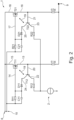
- the 2 shows a circuit diagram of an electronic circuit arrangement 1 for the equal distribution of a current according to a first exemplary embodiment of the invention.
- the basic idea is to distribute the current from an input terminal 6 of the circuit to an output terminal 9 of the circuit to the MOSFETs T11 and T21.
- the MOSFETs T11 and T21 For simplification, in the in 2 shown embodiment shown only two parallel-connected MOSFETs T11 and T21. However, the idea according to the invention can be extended to more than two MOSFETs connected in parallel.
- everyone in 2 MOSFETs T11, T21 shown has a source resistor R13 or R23, and a transistor T12 or T22.
- the transistors T12, T22 are placed in relation to their respective MOSFET T11, T21 in such a way that the transistors T12, T22 can follow the temperature of the respective MOSFET T11, T21 as well as possible. This is ensured by a thermal coupling between the first MOSFET T11 and the first transistor T12 and a thermal coupling 19, also between the second MOSFET T21 and the second transistor T22.
- a thermally conductive medium is provided for the thermal coupling 19 .
- traces of a shared circuit board can be used as the thermally conductive medium.
- the emitter connection 22 of the first transistor T12 and the emitter connection 23 of the second transistor T22 are connected to a current source 2 .
- the current source 2 is dimensioned, for example, for 1 mA per MOSFET T11, T21, so that an average of just under 1 V drops across the resistors R11, R21.
- the control voltage 10 is therefore about 1V higher than the mean value of the gate voltages. In the ideal case, exactly half of the total current flows through the resistors R13 and R23. This means that the current and voltage ratios at R12/R22, T12/T22 and R11/R21 are identical. Furthermore, ideally T11 and T21 as well as T12 and T22 the same temperature. If the balance is now disturbed, eg T11 is subjected to a higher load due to component scatter, the base voltage of T12 increases.
- MOSFET T11, T21 has a poor connection to a heat sink, for example.
- this MOSFET is specifically relieved by the electronic circuit arrangement 1 .
- five MOSFETs T11, T21, . . . connected in parallel can be provided for a total of 20 A rated current.
- the resistors R13 and R23 can be dimensioned with 15 m ⁇ , for example. In the ideal case, each MOSFET T11, T21 carries 4 A and resistors R13, R23 drop 60 mV. If one of the transistors T12, T22 is now 10° C.
- the 3 shows a circuit diagram of an electronic circuit arrangement 1 for dividing a current according to a further exemplary embodiment of the invention.
- the 2 Electronic circuit arrangement 1 shown is in the 3 shown embodiment shown mirrored.
- mirrored means that a second electronic circuit arrangement 3 is provided, NPN transistors being exchanged for PNP transistors and N-MOSFETs for P-MOSFETs, diodes being reversed and voltages and currents being negated.
- In 3 is the combination of circuitry from 2 and the mirrored circuit 3, each with two parallel-connected MOSFETs T11, T21, T13, T16.
- the 3 Circuit arrangement 1, 3 shown comprises an input terminal 7 and a control terminal 11 for a negative branch of the circuit arrangement 3 and an input terminal 8 and a control terminal 12 for a positive branch of the circuit arrangement 1.
- the negative and the positive branch use in the in 3 shown embodiment common source resistors R13, R23.
- the first electronic circuit arrangement 1 and the second electronic circuit arrangement 3 have a common output connection 9 with separate source resistors R13, R23 for the first electronic circuit arrangement 1 and the second electronic circuit arrangement 3.
- the negative and the positive branch each comprise a current source 4, 5.
- the current sources 4, 5 are supplied from voltages which must sufficiently exceed the voltage at the output terminal 9, eg against the input terminal 7, 8.
- the current sources 4, 5 must be sufficient , and to safely cover the adjustment range of the gate voltages for balancing. "Sufficient” or “sufficient” means that the power source (4) is supplied with such a high positive voltage and the power source (5) with such a large negative voltage that for each voltage to be output at the output (9) with with all the expected scattering of the components, the state can be reached in which all MOSFETs are in the Mth state, i.e. the MOSFETs are fully controllable.
- FIG. 12 shows a flowchart of a method for dividing a stream evenly according to an exemplary embodiment of the invention.
- the method starts in step S1 with the provision of an electronic circuit arrangement 1 as previously described.
- step S2 a current present at the input connection 6 is equalized after an output connection 9 by means of the first MOSFET T11 and the second MOSFET T21.
- the gate voltage 14 of the first MOSFET T11 is adjusted using the first transistor T12 and the gate voltage 17 of the second MOSFET T21 is adjusted using the second transistor T22.
- step S3 due to the thermal coupling 19 between the first MOSFET T11 and the first transistor T12 and the thermal coupling 19 between the second MOSFET T21 and the second transistor T22, the current is additionally increased if the temperature between the first MOSFET T11 and the second MOSFET T21 balanced.
Landscapes
- Amplifiers (AREA)
Priority Applications (3)
| Application Number | Priority Date | Filing Date | Title |
|---|---|---|---|
| EP21214298.8A EP4199355B1 (fr) | 2021-12-14 | 2021-12-14 | Agencement du circuit électronique destiné à la distribution de courant |
| CN202211601594.2A CN116264461A (zh) | 2021-12-14 | 2022-12-13 | 用于电流分配的电子电路装置 |
| US18/065,637 US12119812B2 (en) | 2021-12-14 | 2022-12-14 | Electronic circuit arrangement for current distribution |
Applications Claiming Priority (1)
| Application Number | Priority Date | Filing Date | Title |
|---|---|---|---|
| EP21214298.8A EP4199355B1 (fr) | 2021-12-14 | 2021-12-14 | Agencement du circuit électronique destiné à la distribution de courant |
Publications (2)
| Publication Number | Publication Date |
|---|---|
| EP4199355A1 true EP4199355A1 (fr) | 2023-06-21 |
| EP4199355B1 EP4199355B1 (fr) | 2024-09-25 |
Family
ID=78851233
Family Applications (1)
| Application Number | Title | Priority Date | Filing Date |
|---|---|---|---|
| EP21214298.8A Active EP4199355B1 (fr) | 2021-12-14 | 2021-12-14 | Agencement du circuit électronique destiné à la distribution de courant |
Country Status (1)
| Country | Link |
|---|---|
| EP (1) | EP4199355B1 (fr) |
Cited By (1)
| Publication number | Priority date | Publication date | Assignee | Title |
|---|---|---|---|---|
| US20250112629A1 (en) * | 2023-09-28 | 2025-04-03 | Texas Instruments Incorporated | Methods and apparatus to stabilize power fet circuitry |
Citations (4)
| Publication number | Priority date | Publication date | Assignee | Title |
|---|---|---|---|---|
| JPS6198018A (ja) * | 1984-10-19 | 1986-05-16 | Hitachi Ltd | スイツチング回路 |
| JPH09289442A (ja) * | 1996-02-20 | 1997-11-04 | Fuji Electric Co Ltd | 並列接続・可制御半導体素子の電流バランス回路 |
| WO2005015741A2 (fr) * | 2003-08-12 | 2005-02-17 | Philips Intellectual Property & Standards Gmbh | Fonctionnement et circuits d'un circuit de commande et de conversion de puissance |
| US20130002214A1 (en) * | 2011-06-30 | 2013-01-03 | Hon Hai Precision Industry Co., Ltd. | Current balance circuit |
-
2021
- 2021-12-14 EP EP21214298.8A patent/EP4199355B1/fr active Active
Patent Citations (4)
| Publication number | Priority date | Publication date | Assignee | Title |
|---|---|---|---|---|
| JPS6198018A (ja) * | 1984-10-19 | 1986-05-16 | Hitachi Ltd | スイツチング回路 |
| JPH09289442A (ja) * | 1996-02-20 | 1997-11-04 | Fuji Electric Co Ltd | 並列接続・可制御半導体素子の電流バランス回路 |
| WO2005015741A2 (fr) * | 2003-08-12 | 2005-02-17 | Philips Intellectual Property & Standards Gmbh | Fonctionnement et circuits d'un circuit de commande et de conversion de puissance |
| US20130002214A1 (en) * | 2011-06-30 | 2013-01-03 | Hon Hai Precision Industry Co., Ltd. | Current balance circuit |
Non-Patent Citations (1)
| Title |
|---|
| DIVERSE: "Differential Amplifier", WIKIPEDIA, 4 December 2021 (2021-12-04), INTERNET, pages 1 - 10, XP055925476, Retrieved from the Internet <URL:https://en.wikipedia.org/w/index.php?title=Differential_amplifier&oldid=1058519695> [retrieved on 20220527] * |
Cited By (1)
| Publication number | Priority date | Publication date | Assignee | Title |
|---|---|---|---|---|
| US20250112629A1 (en) * | 2023-09-28 | 2025-04-03 | Texas Instruments Incorporated | Methods and apparatus to stabilize power fet circuitry |
Also Published As
| Publication number | Publication date |
|---|---|
| EP4199355B1 (fr) | 2024-09-25 |
Similar Documents
| Publication | Publication Date | Title |
|---|---|---|
| DE69322415T2 (de) | Einschaltstromspitzen- begrenzer | |
| DE69505633T2 (de) | Gleichrichterbrückenschaltung mit aktiven schaltern und einer aktiven steuerschaltung | |
| DE3906927C2 (fr) | ||
| EP4199355B1 (fr) | Agencement du circuit électronique destiné à la distribution de courant | |
| DE1513409A1 (de) | Strombegrenzungsschaltung | |
| DE1513491B2 (de) | Schaltung zur begrenzung hoher gleichspannungen | |
| DE3433817C2 (fr) | ||
| DE69412657T2 (de) | Differentiale Bustreiber | |
| DE102014113715A1 (de) | Eine Schutzschaltung für den Schutz elektronischer Steuerungen vor transienten Automobil-Überspannungsimpulsen | |
| DE102005003643A1 (de) | Strombegrenzer für Ausgangstransistor | |
| DE2738187C2 (de) | Schaltungsanordnung für mehrere auf einem Bipolar-Baustein angeordnete Speicherzellen mit einer Regelschaltung zur Kennlinien-Anpassung der Speicherzellen | |
| DE3545039A1 (de) | Spannungsbegrenzungsschaltung | |
| DE4022253A1 (de) | Strombegrenzungsschaltung | |
| DE102021132970A1 (de) | Elektronische Schaltungsanordnung zur Stromverteilung | |
| DE10205194A1 (de) | Schaltungsanordnung zur Steuerung eines konstanten Stromes durch eine Last | |
| EP0523266A1 (fr) | Miroir à courant intégrable | |
| EP0961403B1 (fr) | Circuit amplificateur intégré compensé en température | |
| DE68925305T2 (de) | Strombegrenzungsschaltung mit Einheitsverstärkung | |
| EP0936525B1 (fr) | Circuit avec ligne caractéristique de diode idéale | |
| DE4113258A1 (de) | Leistungssteuerschaltung mit kurzschlussschutzschaltung | |
| DE2404850C3 (de) | Elektronische Sicherung für einen Gegentakt-Verstarker | |
| DE102023119863B3 (de) | Ausgangsschaltung für eine elektronische Schaltung zur Übermittlung von analogen Ausgangssignalen | |
| DE2304423B2 (de) | Steuerschaltungsanordnung fuer einen thyristor | |
| EP0990199B1 (fr) | Dispositif de reglage | |
| DE10212360B3 (de) | Schaltkreis zum Erzeugen einer einstellbaren Ausgangskennlinie |
Legal Events
| Date | Code | Title | Description |
|---|---|---|---|
| PUAI | Public reference made under article 153(3) epc to a published international application that has entered the european phase |
Free format text: ORIGINAL CODE: 0009012 |
|
| STAA | Information on the status of an ep patent application or granted ep patent |
Free format text: STATUS: THE APPLICATION HAS BEEN PUBLISHED |
|
| AK | Designated contracting states |
Kind code of ref document: A1 Designated state(s): AL AT BE BG CH CY CZ DE DK EE ES FI FR GB GR HR HU IE IS IT LI LT LU LV MC MK MT NL NO PL PT RO RS SE SI SK SM TR |
|
| STAA | Information on the status of an ep patent application or granted ep patent |
Free format text: STATUS: REQUEST FOR EXAMINATION WAS MADE |
|
| 17P | Request for examination filed |
Effective date: 20231221 |
|
| RBV | Designated contracting states (corrected) |
Designated state(s): AL AT BE BG CH CY CZ DE DK EE ES FI FR GB GR HR HU IE IS IT LI LT LU LV MC MK MT NL NO PL PT RO RS SE SI SK SM TR |
|
| GRAP | Despatch of communication of intention to grant a patent |
Free format text: ORIGINAL CODE: EPIDOSNIGR1 |
|
| STAA | Information on the status of an ep patent application or granted ep patent |
Free format text: STATUS: GRANT OF PATENT IS INTENDED |
|
| INTG | Intention to grant announced |
Effective date: 20240513 |
|
| RIC1 | Information provided on ipc code assigned before grant |
Ipc: H03K 17/14 20060101ALI20240430BHEP Ipc: H03K 17/687 20060101ALI20240430BHEP Ipc: H03K 17/12 20060101AFI20240430BHEP |
|
| GRAS | Grant fee paid |
Free format text: ORIGINAL CODE: EPIDOSNIGR3 |
|
| GRAA | (expected) grant |
Free format text: ORIGINAL CODE: 0009210 |
|
| STAA | Information on the status of an ep patent application or granted ep patent |
Free format text: STATUS: THE PATENT HAS BEEN GRANTED |
|
| AK | Designated contracting states |
Kind code of ref document: B1 Designated state(s): AL AT BE BG CH CY CZ DE DK EE ES FI FR GB GR HR HU IE IS IT LI LT LU LV MC MK MT NL NO PL PT RO RS SE SI SK SM TR |
|
| P01 | Opt-out of the competence of the unified patent court (upc) registered |
Free format text: CASE NUMBER: APP_47269/2024 Effective date: 20240820 |
|
| REG | Reference to a national code |
Ref country code: GB Ref legal event code: FG4D Free format text: NOT ENGLISH |
|
| REG | Reference to a national code |
Ref country code: CH Ref legal event code: EP |
|
| REG | Reference to a national code |
Ref country code: DE Ref legal event code: R096 Ref document number: 502021005242 Country of ref document: DE |
|
| REG | Reference to a national code |
Ref country code: IE Ref legal event code: FG4D Free format text: LANGUAGE OF EP DOCUMENT: GERMAN |
|
| REG | Reference to a national code |
Ref country code: LT Ref legal event code: MG9D |
|
| PG25 | Lapsed in a contracting state [announced via postgrant information from national office to epo] |
Ref country code: NO Free format text: LAPSE BECAUSE OF FAILURE TO SUBMIT A TRANSLATION OF THE DESCRIPTION OR TO PAY THE FEE WITHIN THE PRESCRIBED TIME-LIMIT Effective date: 20241225 |
|
| PG25 | Lapsed in a contracting state [announced via postgrant information from national office to epo] |
Ref country code: GR Free format text: LAPSE BECAUSE OF FAILURE TO SUBMIT A TRANSLATION OF THE DESCRIPTION OR TO PAY THE FEE WITHIN THE PRESCRIBED TIME-LIMIT Effective date: 20241226 Ref country code: FI Free format text: LAPSE BECAUSE OF FAILURE TO SUBMIT A TRANSLATION OF THE DESCRIPTION OR TO PAY THE FEE WITHIN THE PRESCRIBED TIME-LIMIT Effective date: 20240925 |
|
| PG25 | Lapsed in a contracting state [announced via postgrant information from national office to epo] |
Ref country code: BG Free format text: LAPSE BECAUSE OF FAILURE TO SUBMIT A TRANSLATION OF THE DESCRIPTION OR TO PAY THE FEE WITHIN THE PRESCRIBED TIME-LIMIT Effective date: 20240925 |
|
| PG25 | Lapsed in a contracting state [announced via postgrant information from national office to epo] |
Ref country code: LV Free format text: LAPSE BECAUSE OF FAILURE TO SUBMIT A TRANSLATION OF THE DESCRIPTION OR TO PAY THE FEE WITHIN THE PRESCRIBED TIME-LIMIT Effective date: 20240925 |
|
| PG25 | Lapsed in a contracting state [announced via postgrant information from national office to epo] |
Ref country code: RS Free format text: LAPSE BECAUSE OF FAILURE TO SUBMIT A TRANSLATION OF THE DESCRIPTION OR TO PAY THE FEE WITHIN THE PRESCRIBED TIME-LIMIT Effective date: 20241225 |
|
| REG | Reference to a national code |
Ref country code: NL Ref legal event code: MP Effective date: 20240925 |
|
| PG25 | Lapsed in a contracting state [announced via postgrant information from national office to epo] |
Ref country code: RS Free format text: LAPSE BECAUSE OF FAILURE TO SUBMIT A TRANSLATION OF THE DESCRIPTION OR TO PAY THE FEE WITHIN THE PRESCRIBED TIME-LIMIT Effective date: 20241225 Ref country code: NO Free format text: LAPSE BECAUSE OF FAILURE TO SUBMIT A TRANSLATION OF THE DESCRIPTION OR TO PAY THE FEE WITHIN THE PRESCRIBED TIME-LIMIT Effective date: 20241225 Ref country code: LV Free format text: LAPSE BECAUSE OF FAILURE TO SUBMIT A TRANSLATION OF THE DESCRIPTION OR TO PAY THE FEE WITHIN THE PRESCRIBED TIME-LIMIT Effective date: 20240925 Ref country code: GR Free format text: LAPSE BECAUSE OF FAILURE TO SUBMIT A TRANSLATION OF THE DESCRIPTION OR TO PAY THE FEE WITHIN THE PRESCRIBED TIME-LIMIT Effective date: 20241226 Ref country code: FI Free format text: LAPSE BECAUSE OF FAILURE TO SUBMIT A TRANSLATION OF THE DESCRIPTION OR TO PAY THE FEE WITHIN THE PRESCRIBED TIME-LIMIT Effective date: 20240925 Ref country code: BG Free format text: LAPSE BECAUSE OF FAILURE TO SUBMIT A TRANSLATION OF THE DESCRIPTION OR TO PAY THE FEE WITHIN THE PRESCRIBED TIME-LIMIT Effective date: 20240925 |
|
| PG25 | Lapsed in a contracting state [announced via postgrant information from national office to epo] |
Ref country code: NL Free format text: LAPSE BECAUSE OF FAILURE TO SUBMIT A TRANSLATION OF THE DESCRIPTION OR TO PAY THE FEE WITHIN THE PRESCRIBED TIME-LIMIT Effective date: 20240925 |
|
| PG25 | Lapsed in a contracting state [announced via postgrant information from national office to epo] |
Ref country code: IS Free format text: LAPSE BECAUSE OF FAILURE TO SUBMIT A TRANSLATION OF THE DESCRIPTION OR TO PAY THE FEE WITHIN THE PRESCRIBED TIME-LIMIT Effective date: 20250125 Ref country code: PT Free format text: LAPSE BECAUSE OF FAILURE TO SUBMIT A TRANSLATION OF THE DESCRIPTION OR TO PAY THE FEE WITHIN THE PRESCRIBED TIME-LIMIT Effective date: 20250127 |
|
| PG25 | Lapsed in a contracting state [announced via postgrant information from national office to epo] |
Ref country code: RO Free format text: LAPSE BECAUSE OF FAILURE TO SUBMIT A TRANSLATION OF THE DESCRIPTION OR TO PAY THE FEE WITHIN THE PRESCRIBED TIME-LIMIT Effective date: 20240925 Ref country code: SM Free format text: LAPSE BECAUSE OF FAILURE TO SUBMIT A TRANSLATION OF THE DESCRIPTION OR TO PAY THE FEE WITHIN THE PRESCRIBED TIME-LIMIT Effective date: 20240925 |
|
| PG25 | Lapsed in a contracting state [announced via postgrant information from national office to epo] |
Ref country code: ES Free format text: LAPSE BECAUSE OF FAILURE TO SUBMIT A TRANSLATION OF THE DESCRIPTION OR TO PAY THE FEE WITHIN THE PRESCRIBED TIME-LIMIT Effective date: 20240925 |
|
| PG25 | Lapsed in a contracting state [announced via postgrant information from national office to epo] |
Ref country code: EE Free format text: LAPSE BECAUSE OF FAILURE TO SUBMIT A TRANSLATION OF THE DESCRIPTION OR TO PAY THE FEE WITHIN THE PRESCRIBED TIME-LIMIT Effective date: 20240925 |
|
| PG25 | Lapsed in a contracting state [announced via postgrant information from national office to epo] |
Ref country code: CZ Free format text: LAPSE BECAUSE OF FAILURE TO SUBMIT A TRANSLATION OF THE DESCRIPTION OR TO PAY THE FEE WITHIN THE PRESCRIBED TIME-LIMIT Effective date: 20240925 Ref country code: PL Free format text: LAPSE BECAUSE OF FAILURE TO SUBMIT A TRANSLATION OF THE DESCRIPTION OR TO PAY THE FEE WITHIN THE PRESCRIBED TIME-LIMIT Effective date: 20240925 |
|
| PG25 | Lapsed in a contracting state [announced via postgrant information from national office to epo] |
Ref country code: SK Free format text: LAPSE BECAUSE OF FAILURE TO SUBMIT A TRANSLATION OF THE DESCRIPTION OR TO PAY THE FEE WITHIN THE PRESCRIBED TIME-LIMIT Effective date: 20240925 Ref country code: IT Free format text: LAPSE BECAUSE OF FAILURE TO SUBMIT A TRANSLATION OF THE DESCRIPTION OR TO PAY THE FEE WITHIN THE PRESCRIBED TIME-LIMIT Effective date: 20240925 |
|
| REG | Reference to a national code |
Ref country code: DE Ref legal event code: R097 Ref document number: 502021005242 Country of ref document: DE |
|
| PG25 | Lapsed in a contracting state [announced via postgrant information from national office to epo] |
Ref country code: MC Free format text: LAPSE BECAUSE OF FAILURE TO SUBMIT A TRANSLATION OF THE DESCRIPTION OR TO PAY THE FEE WITHIN THE PRESCRIBED TIME-LIMIT Effective date: 20240925 |
|
| PG25 | Lapsed in a contracting state [announced via postgrant information from national office to epo] |
Ref country code: DK Free format text: LAPSE BECAUSE OF FAILURE TO SUBMIT A TRANSLATION OF THE DESCRIPTION OR TO PAY THE FEE WITHIN THE PRESCRIBED TIME-LIMIT Effective date: 20240925 |
|
| REG | Reference to a national code |
Ref country code: CH Ref legal event code: PL |
|
| PLBE | No opposition filed within time limit |
Free format text: ORIGINAL CODE: 0009261 |
|
| STAA | Information on the status of an ep patent application or granted ep patent |
Free format text: STATUS: NO OPPOSITION FILED WITHIN TIME LIMIT |
|
| PG25 | Lapsed in a contracting state [announced via postgrant information from national office to epo] |
Ref country code: LU Free format text: LAPSE BECAUSE OF NON-PAYMENT OF DUE FEES Effective date: 20241214 |
|
| 26N | No opposition filed |
Effective date: 20250626 |
|
| PG25 | Lapsed in a contracting state [announced via postgrant information from national office to epo] |
Ref country code: SE Free format text: LAPSE BECAUSE OF FAILURE TO SUBMIT A TRANSLATION OF THE DESCRIPTION OR TO PAY THE FEE WITHIN THE PRESCRIBED TIME-LIMIT Effective date: 20240925 |
|
| REG | Reference to a national code |
Ref country code: BE Ref legal event code: MM Effective date: 20241231 |
|
| PG25 | Lapsed in a contracting state [announced via postgrant information from national office to epo] |
Ref country code: BE Free format text: LAPSE BECAUSE OF NON-PAYMENT OF DUE FEES Effective date: 20241231 |
|
| PG25 | Lapsed in a contracting state [announced via postgrant information from national office to epo] |
Ref country code: FR Free format text: LAPSE BECAUSE OF NON-PAYMENT OF DUE FEES Effective date: 20241231 |
|
| PG25 | Lapsed in a contracting state [announced via postgrant information from national office to epo] |
Ref country code: CH Free format text: LAPSE BECAUSE OF NON-PAYMENT OF DUE FEES Effective date: 20241231 |
|
| PG25 | Lapsed in a contracting state [announced via postgrant information from national office to epo] |
Ref country code: IE Free format text: LAPSE BECAUSE OF NON-PAYMENT OF DUE FEES Effective date: 20241214 |
|
| PGFP | Annual fee paid to national office [announced via postgrant information from national office to epo] |
Ref country code: DE Payment date: 20251211 Year of fee payment: 5 |
|
| PGFP | Annual fee paid to national office [announced via postgrant information from national office to epo] |
Ref country code: AT Payment date: 20260113 Year of fee payment: 5 |
|
| PG25 | Lapsed in a contracting state [announced via postgrant information from national office to epo] |
Ref country code: HR Free format text: LAPSE BECAUSE OF FAILURE TO SUBMIT A TRANSLATION OF THE DESCRIPTION OR TO PAY THE FEE WITHIN THE PRESCRIBED TIME-LIMIT Effective date: 20240925 |
|
| REG | Reference to a national code |
Ref country code: DE Ref legal event code: R081 Ref document number: 502021005242 Country of ref document: DE Owner name: DSPACE SE & CO KG, DE Free format text: FORMER OWNER: DSPACE GMBH, 33102 PADERBORN, DE |