EP4199662A1 - Leiterplatte und herstellungsverfahren dafür sowie endgerätevorrichtung - Google Patents
Leiterplatte und herstellungsverfahren dafür sowie endgerätevorrichtung Download PDFInfo
- Publication number
- EP4199662A1 EP4199662A1 EP22857003.2A EP22857003A EP4199662A1 EP 4199662 A1 EP4199662 A1 EP 4199662A1 EP 22857003 A EP22857003 A EP 22857003A EP 4199662 A1 EP4199662 A1 EP 4199662A1
- Authority
- EP
- European Patent Office
- Prior art keywords
- pad
- liquid metal
- metal body
- radio frequency
- circuit board
- Prior art date
- Legal status (The legal status is an assumption and is not a legal conclusion. Google has not performed a legal analysis and makes no representation as to the accuracy of the status listed.)
- Granted
Links
Images


Classifications
-
- H—ELECTRICITY
- H05—ELECTRIC TECHNIQUES NOT OTHERWISE PROVIDED FOR
- H05K—PRINTED CIRCUITS; CASINGS OR CONSTRUCTIONAL DETAILS OF ELECTRIC APPARATUS; MANUFACTURE OF ASSEMBLAGES OF ELECTRICAL COMPONENTS
- H05K1/00—Printed circuits
- H05K1/02—Details
- H05K1/0266—Marks, test patterns or identification means
- H05K1/0268—Marks, test patterns or identification means for electrical inspection or testing
-
- H—ELECTRICITY
- H05—ELECTRIC TECHNIQUES NOT OTHERWISE PROVIDED FOR
- H05K—PRINTED CIRCUITS; CASINGS OR CONSTRUCTIONAL DETAILS OF ELECTRIC APPARATUS; MANUFACTURE OF ASSEMBLAGES OF ELECTRICAL COMPONENTS
- H05K1/00—Printed circuits
- H05K1/02—Details
- H05K1/0286—Programmable, customizable or modifiable circuits
- H05K1/0293—Individual printed conductors which are adapted for modification, e.g. fusable or breakable conductors, printed switches
-
- H—ELECTRICITY
- H05—ELECTRIC TECHNIQUES NOT OTHERWISE PROVIDED FOR
- H05K—PRINTED CIRCUITS; CASINGS OR CONSTRUCTIONAL DETAILS OF ELECTRIC APPARATUS; MANUFACTURE OF ASSEMBLAGES OF ELECTRICAL COMPONENTS
- H05K1/00—Printed circuits
- H05K1/02—Details
- H05K1/11—Printed elements for providing electric connections to or between printed circuits
- H05K1/115—Via connections; Lands around holes or via connections
- H05K1/116—Lands, clearance holes or other lay-out details concerning the surrounding of a via
-
- H—ELECTRICITY
- H05—ELECTRIC TECHNIQUES NOT OTHERWISE PROVIDED FOR
- H05K—PRINTED CIRCUITS; CASINGS OR CONSTRUCTIONAL DETAILS OF ELECTRIC APPARATUS; MANUFACTURE OF ASSEMBLAGES OF ELECTRICAL COMPONENTS
- H05K3/00—Apparatus or processes for manufacturing printed circuits
- H05K3/30—Assembling printed circuits with electric components, e.g. with resistors
- H05K3/32—Assembling printed circuits with electric components, e.g. with resistors electrically connecting electric components or wires to printed circuits
- H05K3/34—Assembling printed circuits with electric components, e.g. with resistors electrically connecting electric components or wires to printed circuits by soldering
- H05K3/3465—Application of solder
- H05K3/3485—Application of solder paste, slurry or powder
-
- H—ELECTRICITY
- H05—ELECTRIC TECHNIQUES NOT OTHERWISE PROVIDED FOR
- H05K—PRINTED CIRCUITS; CASINGS OR CONSTRUCTIONAL DETAILS OF ELECTRIC APPARATUS; MANUFACTURE OF ASSEMBLAGES OF ELECTRICAL COMPONENTS
- H05K9/00—Screening of apparatus or components against electric or magnetic fields
- H05K9/0007—Casings
- H05K9/002—Casings with localised screening
- H05K9/0022—Casings with localised screening of components mounted on printed circuit boards [PCB]
- H05K9/0024—Shield cases mounted on a PCB, e.g. cans or caps or conformal shields
-
- H—ELECTRICITY
- H05—ELECTRIC TECHNIQUES NOT OTHERWISE PROVIDED FOR
- H05K—PRINTED CIRCUITS; CASINGS OR CONSTRUCTIONAL DETAILS OF ELECTRIC APPARATUS; MANUFACTURE OF ASSEMBLAGES OF ELECTRICAL COMPONENTS
- H05K1/00—Printed circuits
- H05K1/02—Details
- H05K1/0213—Electrical arrangements not otherwise provided for
- H05K1/0237—High frequency adaptations
- H05K1/0243—Printed circuits associated with mounted high frequency components
-
- H—ELECTRICITY
- H05—ELECTRIC TECHNIQUES NOT OTHERWISE PROVIDED FOR
- H05K—PRINTED CIRCUITS; CASINGS OR CONSTRUCTIONAL DETAILS OF ELECTRIC APPARATUS; MANUFACTURE OF ASSEMBLAGES OF ELECTRICAL COMPONENTS
- H05K1/00—Printed circuits
- H05K1/02—Details
- H05K1/11—Printed elements for providing electric connections to or between printed circuits
- H05K1/111—Pads for surface mounting, e.g. lay-out
-
- H—ELECTRICITY
- H05—ELECTRIC TECHNIQUES NOT OTHERWISE PROVIDED FOR
- H05K—PRINTED CIRCUITS; CASINGS OR CONSTRUCTIONAL DETAILS OF ELECTRIC APPARATUS; MANUFACTURE OF ASSEMBLAGES OF ELECTRICAL COMPONENTS
- H05K2201/00—Indexing scheme relating to printed circuits covered by H05K1/00
- H05K2201/03—Conductive materials
- H05K2201/0332—Structure of the conductor
- H05K2201/0335—Layered conductors or foils
- H05K2201/035—Paste overlayer, i.e. conductive paste or solder paste over conductive layer
-
- H—ELECTRICITY
- H05—ELECTRIC TECHNIQUES NOT OTHERWISE PROVIDED FOR
- H05K—PRINTED CIRCUITS; CASINGS OR CONSTRUCTIONAL DETAILS OF ELECTRIC APPARATUS; MANUFACTURE OF ASSEMBLAGES OF ELECTRICAL COMPONENTS
- H05K2201/00—Indexing scheme relating to printed circuits covered by H05K1/00
- H05K2201/10—Details of components or other objects attached to or integrated in a printed circuit board
- H05K2201/10007—Types of components
- H05K2201/10098—Components for radio transmission, e.g. radio frequency identification [RFID] tag, printed or non-printed antennas
-
- H—ELECTRICITY
- H05—ELECTRIC TECHNIQUES NOT OTHERWISE PROVIDED FOR
- H05K—PRINTED CIRCUITS; CASINGS OR CONSTRUCTIONAL DETAILS OF ELECTRIC APPARATUS; MANUFACTURE OF ASSEMBLAGES OF ELECTRICAL COMPONENTS
- H05K2203/00—Indexing scheme relating to apparatus or processes for manufacturing printed circuits covered by H05K3/00
- H05K2203/01—Tools for processing; Objects used during processing
- H05K2203/0104—Tools for processing; Objects used during processing for patterning or coating
- H05K2203/0126—Dispenser, e.g. for solder paste, for supplying conductive paste for screen printing or for filling holes
-
- H—ELECTRICITY
- H05—ELECTRIC TECHNIQUES NOT OTHERWISE PROVIDED FOR
- H05K—PRINTED CIRCUITS; CASINGS OR CONSTRUCTIONAL DETAILS OF ELECTRIC APPARATUS; MANUFACTURE OF ASSEMBLAGES OF ELECTRICAL COMPONENTS
- H05K2203/00—Indexing scheme relating to apparatus or processes for manufacturing printed circuits covered by H05K3/00
- H05K2203/14—Related to the order of processing steps
- H05K2203/1461—Applying or finishing the circuit pattern after another process, e.g. after filling of vias with conductive paste, after making printed resistors
-
- H—ELECTRICITY
- H05—ELECTRIC TECHNIQUES NOT OTHERWISE PROVIDED FOR
- H05K—PRINTED CIRCUITS; CASINGS OR CONSTRUCTIONAL DETAILS OF ELECTRIC APPARATUS; MANUFACTURE OF ASSEMBLAGES OF ELECTRICAL COMPONENTS
- H05K2203/00—Indexing scheme relating to apparatus or processes for manufacturing printed circuits covered by H05K3/00
- H05K2203/16—Inspection; Monitoring; Aligning
- H05K2203/162—Testing a finished product, e.g. heat cycle testing of solder joints
-
- H—ELECTRICITY
- H05—ELECTRIC TECHNIQUES NOT OTHERWISE PROVIDED FOR
- H05K—PRINTED CIRCUITS; CASINGS OR CONSTRUCTIONAL DETAILS OF ELECTRIC APPARATUS; MANUFACTURE OF ASSEMBLAGES OF ELECTRICAL COMPONENTS
- H05K2203/00—Indexing scheme relating to apparatus or processes for manufacturing printed circuits covered by H05K3/00
- H05K2203/17—Post-manufacturing processes
- H05K2203/173—Adding connections between adjacent pads or conductors, e.g. for modifying or repairing
-
- H—ELECTRICITY
- H05—ELECTRIC TECHNIQUES NOT OTHERWISE PROVIDED FOR
- H05K—PRINTED CIRCUITS; CASINGS OR CONSTRUCTIONAL DETAILS OF ELECTRIC APPARATUS; MANUFACTURE OF ASSEMBLAGES OF ELECTRICAL COMPONENTS
- H05K3/00—Apparatus or processes for manufacturing printed circuits
- H05K3/22—Secondary treatment of printed circuits
Definitions
- This application relates to the technical field of terminals, and in particular, to a circuit board and a manufacturing method thereof, and a terminal device.
- a radio frequency circuit is an important part in a circuit board of a terminal device such as a mobile phone, and usually includes a radio frequency front-end circuit and a radio frequency back-end circuit.
- the radio frequency front-end circuit includes a large quantity of components and has a relatively complex composition. Therefore, during actual production of the circuit board, it is required to test the radio frequency front-end circuit to detect quality and soldering problems of components in the radio frequency circuit.
- FIG. 1 is a schematic diagram showing testing of a circuit board of a current terminal device.
- the circuit board of the terminal device includes a radio frequency front-end circuit 11, a radio frequency back-end circuit 12, and a switch test socket 17 connected between the radio frequency front-end circuit 11 and the radio frequency back-end circuit 12.
- a test end 410 of a radio frequency test instrument 400 is inserted into the switch test socket 17 to disconnect the radio frequency front-end circuit 11 from the radio frequency back-end circuit 12, and the test end 410 is electrically connected to the radio frequency front-end circuit 11 to introduce a signal from the radio frequency front-end circuit 11 into the radio frequency test instrument 400 for testing.
- the test end 410 is pulled out of the switch test socket 17 to reconnect the radio frequency front-end circuit 11 to the radio frequency back-end circuit 12 to ensure a normal function of the circuit board.
- the radio frequency switch test socket 17 on the foregoing circuit board usually has no other function after the testing is completed, which occupies a layout area on the circuit board, and increases device costs of the terminal device.
- a related technology discloses a circuit board, in which two pads are used instead of the switch test socket. One of the pads is connected to a radio frequency front-end circuit, and the other is connected to a radio frequency back-end circuit.
- a test end of a radio frequency test instrument is connected to one of the pads, to introduce a signal from the radio frequency front-end circuit into the radio frequency test instrument for testing.
- serial devices are soldered between the two pads by using a low-temperature reflow soldering process, so that the radio frequency front-end circuit is connected to the radio frequency back-end circuit.
- the series devices are soldered between the two pads by using the low-temperature reflow soldering process.
- Low-temperature solder paste is required for soldering
- high-temperature solder paste is usually used for soldering other devices on the circuit board of the terminal device, which increases a risk of mixing up the solder paste.
- the high-temperature solder paste may be easily mixed up for soldering during soldering of the series devices, which increases a probability of a soldering defect, and reduces reliability of the connection between the radio frequency front-end circuit and the radio frequency back-end circuit.
- Embodiments of this application provide a circuit board and a manufacturing method thereof, and a terminal device, to resolve the problem of low reliability of connection between a radio frequency front-end circuit and a radio frequency back-end circuit in a circuit board of a terminal device in a related technology.
- an embodiment of this application provides a circuit board, including a substrate and a liquid metal body, where the substrate is provided with a radio frequency front-end circuit, a radio frequency back-end circuit, and a pad group, where the pad group includes a first pad electrically connected to the radio frequency front-end circuit and a second pad electrically connected to the radio frequency back-end circuit, and the second pad is spaced apart from the first pad; and the liquid metal body is arranged at a position of the pad group and connects the first pad to the second pad, so as to electrically connect the radio frequency front-end circuit to the radio frequency back-end circuit.
- a process for connection between the first pad and the second pad is simpler, and low-temperature solder paste is not needed for soldering, so that a soldering defect caused by mixing up solder paste is prevented, thereby improving reliability of the connection between the first pad and the second pad, and improving reliability of the connection between the radio frequency front-end circuit and the radio frequency back-end circuit.
- the liquid metal body is arranged on a side that is of the pad group and that is far away from the substrate, and is in contact with the first pad and the second pad.
- the liquid metal body is prevented from being in contact with the substrate, thereby reducing a risk that a line on the substrate is short-circuited by the liquid metal body.
- the first pad includes a first pad surface on a side far away from the substrate, and the second pad includes a second pad surface on a side far away from the substrate; and the liquid metal body has a layered structure, and is laminated with the first pad surface and the first pad surface.
- the first pad surface is flush with the second pad surface.
- the first pad and the second pad can be prevented from forming a step, so that the liquid metal body can be easily arranged on the first pad surface and the second pad surface.
- the liquid metal body is flush with a side edge that is of the first pad surface and that is far away from the second pad.
- the contact area between the liquid metal body and the second pad surface can be maximized, thereby better reducing the impedance of the liquid metal body.
- the liquid metal body is flush with a side edge that is of the second pad surface and that is far away from the first pad.
- the contact area between the liquid metal body and the second pad surface can be maximized, thereby better reducing the impedance of the liquid metal body.
- the circuit board further includes a first insulation layer, and the first insulation layer fills a gap between the first pad and the second pad.
- the first insulation layer can support a part that is of the liquid metal body and that is opposite to the gap between the first pad and the second pad, so as to better prevent the liquid metal body from being in contact with the substrate.
- the liquid metal body fills the gap between the first pad and the second pad.
- the liquid metal body can be well prevented from being separated from the pad group and moving to another position when the terminal device shakes.
- the circuit board further includes a second insulation layer, and the second insulation layer is arranged at a position of the liquid metal body to cover the liquid metal body.
- the liquid metal body can be prevented from being in contact with and short-circuited with an electronic device around the pad group.
- the liquid metal body has a layered structure, and the second insulation layer is stacked on a side that is of the liquid metal body and that is far away from the substrate.
- the second insulation layer can be easily arranged on the liquid metal body, so that a contact area between the second insulation layer and the liquid metal body is large, and the second insulation layer will not be easily separated from the liquid metal body.
- the second insulation layer is a heat curing adhesive layer or an ultraviolet curing adhesive layer.
- the second insulation layer has a certain mechanical strength, so that the position of the liquid metal body can be well limited at the pad group.
- a plurality of pad groups are provided, and the plurality of pad groups are arranged side by side.
- a test end of a radio frequency test instrument can be easily connected to the first pads of the plurality of pad groups, and reliability of connection between the test end and the pad group is improved.
- the circuit board further includes a first shielding can, and the first shielding can covers a region of the substrate provided with the radio frequency front-end circuit.
- the circuit board further includes a second shielding can, and the second shielding can covers a region of the substrate provided with the radio frequency back-end circuit.
- electromagnetic interference of another device on the substrate to the radio frequency back-end circuit during operation can be shielded, and electromagnetic interference of the radio frequency back-end circuit to another device around during operation can also be shielded.
- an embodiment of this application provides a terminal device, including a housing, an antenna, and the circuit board according to the first aspect, where the circuit board is arranged in the housing, and the antenna is electrically connected to a radio frequency back-end circuit of the circuit board.
- an embodiment of this application provides a method for manufacturing a circuit board, including: providing a substrate, where the substrate is provided with a radio frequency front-end circuit, a radio frequency back-end circuit, and a pad group, where the pad group includes a first pad electrically connected to the radio frequency front-end circuit and a second pad electrically connected to the radio frequency back-end circuit, and the second pad is spaced apart from the first pad; electrically connecting a test end of a radio frequency test instrument to the first pad, to test the radio frequency front-end circuit; and arranging a liquid metal body at a position of the pad group after the testing of the radio frequency front-end circuit is completed, to connect the first pad to the second pad, so as to electrically connect the radio frequency front-end circuit to the radio frequency back-end circuit.
- the arranging a liquid metal body at a position of the pad group after the testing of the radio frequency front-end circuit is completed, to connect the first pad to the second pad includes: arranging the liquid metal body on a side that is of the pad group and that is far away from the substrate, to enable the liquid metal body to be in contact with the first pad and the second pad.
- the liquid metal body is prevented from being in contact with the substrate, thereby reducing a risk that a line on the substrate is short-circuited by the liquid metal body.
- the method before the arranging the liquid metal body on a side that is of the pad group and that is far away from the substrate, the method further includes: filling a gap between the first pad and the second pad with an insulating material, to form a first insulation layer.
- the first insulation layer can support a part that is of the liquid metal body and that is opposite to a space between the first pad and the second pad, so as to better prevent the liquid metal body from being in contact with the substrate.
- the arranging the liquid metal body on a side that is of the pad group and that is far away from the substrate, to enable the liquid metal body to be in contact with the first pad and the second pad includes: laminating a mask with a mask hole on an upper layer of the substrate, so that the pad group is located in the mask hole; and coating the mask hole with a liquid metal material, to form the liquid metal body on the side that is of the pad group and that is far away from the substrate.
- the arranging a liquid metal body at a position of the pad group, to connect the first pad to the second pad includes: filling the gap between the first pad and the second pad with a liquid metal material, to form the liquid metal body.
- the liquid metal body can be well prevented from being separated from the pad group and moving to another position when the terminal device shakes.
- the filling the gap between the first pad and the second pad with a liquid metal material, to form the liquid metal body includes: laminating a mask with a mask hole on an upper layer of the substrate, so that the pad group is located in the mask hole; and coating the mask hole with a liquid metal material, to form the liquid metal body in the gap between the first pad and the second pad.
- the method further includes: coating the position of the liquid metal body with an insulating material, to form a second insulation layer covering the liquid metal body.
- the liquid metal body can be prevented from being in contact with and short-circuited with an electronic device around the pad group.
- the coating the position of the liquid metal body with an insulating material, to form a second insulation layer covering the liquid metal body includes: coating the position of the liquid metal body with an insulating adhesive material, and then curing to form the second insulation layer.
- the second insulation layer formed by curing the insulating adhesive material has a certain mechanical strength, so that the position of the liquid metal body can be well limited at the pad group.
- first and second are used for descriptive purposes only, and cannot be construed as indicating or implying relative importance or implicitly indicating the quantity of technical features indicated. Therefore, the features defined with “first” and “second” may explicitly or implicitly include one or more of the features.
- electrical connection should be understood in a broad sense, for example, as a direct connection for current conduction or as a capacitive coupling for electric energy conduction.
- Embodiments of this application provide a circuit board and a manufacturing method thereof, and a terminal device, to improve reliability of connection between a radio frequency front-end circuit and a radio frequency back-end circuit by using a liquid metal body instead of serial devices soldered to a pad in a related technology.
- the terminal device in the embodiments of this application may be a terminal device with an antenna structure, such as a mobile phone, a tablet computer, an e-reader, a wearable device (such as a smartwatch), a POS (point of sales terminal, point of sales information management system) terminal, a personal digital assistant (personal digital assistant, PDA), a vehicle-mounted device, or an Internet TV
- a terminal device with an antenna structure such as a mobile phone, a tablet computer, an e-reader, a wearable device (such as a smartwatch), a POS (point of sales terminal, point of sales information management system) terminal, a personal digital assistant (personal digital assistant, PDA), a vehicle-mounted device, or an Internet TV
- a circuit board of the terminal device in the embodiments of this application is described below in detail by using a mobile phone as an example.
- Another type of terminal device may be specifically arranged with reference to a design concept of a circuit board in the mobile phone embodiments, and details are not described herein again.
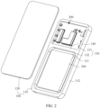
- FIG. 2 is an exploded view of a mobile phone in some embodiments of this application.
- the mobile phone includes a housing 100, a circuit board 200, and a battery 300.
- the housing 100 includes a front housing 110 (also referred to as a middle frame) and a rear cover 120 (also referred to as a battery cover).
- the front housing 110 includes a bottom wall 111 and a side wall 112 arranged on an edge of the bottom wall 111.
- the rear cover 120 is buckled on the front housing 110, and the rear cover 120 forms an accommodating space 130 with the bottom wall 111 and the side wall 112 of the front housing 110.
- the accommodating space 130 includes a circuit board accommodating space 131 and a battery accommodating space 132 separated by a partition wall 140.
- the circuit board 200 is arranged in the circuit board accommodating space 131, and the battery 300 is arranged in the battery accommodating space 132 and is electrically connected to the circuit board 200 by using an electrical connector (not shown in the figure).
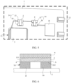
- FIG. 3 is a schematic diagram of a structure of a circuit board 200 in FIG. 2 ;
- FIG. 4 is a partial schematic diagram of FIG. 3 ;
- FIG. 5 is a schematic diagram of a structure of the circuit board 200 in FIG. 3 after removal of a second insulation layer 4.
- the circuit board 200 includes a substrate 1 and a liquid metal body 2.
- the substrate 1 is provided with a radio frequency front-end circuit 11, a radio frequency back-end circuit 12, an antenna spring 13, and a pad group 14, where the pad group 14 includes a first pad 15 electrically connected to the radio frequency front-end circuit 11 and a second pad 16 electrically connected to the radio frequency back-end circuit 12, and the second pad 16 is spaced apart from the first pad 15.
- Contour shapes of the first pad 15 and the second pad 16 are rectangular (as shown in FIG. 5 ), but are not limited thereto, and contour shapes of the first pad 15 and the second pad 16 may alternatively be circular, elliptical, or the like.
- the terminal device further includes an antenna.
- the antenna includes an antenna radiator arranged in the circuit board accommodating space 131, and the antenna radiator is electrically connected to the radio frequency back-end circuit 12 by using the antenna spring 13.
- a quantity of antenna springs 13 may be one or more, specifically depending on a quantity of antenna radiators.
- the foregoing substrate 1 is a circuit board 200 without any circuit device or chip soldered.
- the radio frequency front-end circuit 11 refers to a part of a circuit between the antenna and an intermediate frequency (or baseband) circuit, and in this part of the circuit, a signal is transmitted in the form of a radio frequency.
- the radio frequency front-end circuit 11 usually includes an amplifier, a filter, a frequency converter, and the like.
- the radio frequency back-end circuit 12 includes, but is not limited to, an antenna matching circuit.
- the liquid metal body 2 is arranged at a position of the pad group 14 and connects the first pad 15 to the second pad 16, so as to electrically connect the radio frequency front-end circuit 11 to the radio frequency back-end circuit 12.
- a material of the liquid metal body 2 is a liquid metal material, which is a general name of a kind of metal materials that are in a liquid state at a low temperature.
- the liquid metal material not only has extremely strong thermal conductivity and electrical conductivity of metal materials, but also has certain fluidity.
- the liquid metal material may be made into paste, which is sticky in texture and has strong adsorbability.
- the material of the liquid metal body may be a low-melting-point metal, such as gallium (Ga) as well as sodium (Na), potassium (K), and lithium (Li) among alkali metals, or may be a low-melting-point alloy, such as a gallium metal alloy, which is not specifically limited herein.
- a low-melting-point metal such as gallium (Ga) as well as sodium (Na), potassium (K), and lithium (Li) among alkali metals
- a low-melting-point alloy such as a gallium metal alloy, which is not specifically limited herein.
- Table 1 shows electrical parameters when the liquid metal body is a gallium metal alloy. According to data in Table 1, it can be learned that electrical conductivity and impedance of the liquid metal body 2 can fully meet a use requirement for a radio frequency circuit. Table 1 Electrical parameters when the liquid metal body 2 is a gallium metal alloy Physical item Unit Numerical value ⁇ ⁇ mm 2 /m 0.363 I m 0.00115 S mm 2 0.083 R ⁇ 0.05
- R ⁇ I / S , where ⁇ is a resistivity of the liquid metal body 2; I is a length of the liquid metal body 2; S is a cross-sectional area of the liquid metal body 2; and R is impedance of the liquid metal body 2.
- the liquid metal body 2 is arranged at the position of the pad group 14, and the first pad 15 is connected to the second pad 16.
- the connection can be completed by arranging the liquid metal body 2 at the first pad 15 and the second pad 16, a process for the connection between the first pad 15 and the second pad 16 is simpler, and low-temperature solder paste is not needed for soldering, so that a soldering defect caused by mixing up solder paste is prevented, thereby improving reliability of the connection between the first pad 15 and the second pad 16, and improving reliability of the connection between the radio frequency front-end circuit 11 and the radio frequency back-end circuit 12.
- the liquid metal material can be applied onto the pad group 14 by using an existing dot coating device to form the liquid metal body 2, without an additional device, so that a process route of the circuit board 200 is simpler, which reduces manufacturing costs of the circuit board 200.
- FIG. 5 and FIG. 6 show a first embodiment of a position of the liquid metal body 2 at the pad group 14, and FIG. 6 shows a sectional view of the circuit board 200 in FIG. 4 at the pad group 14.
- the liquid metal body 2 is arranged on a side that is of the pad group 14 and that is far away from the substrate 1, and is in contact with the first pad 15 and the second pad 16.
- the arrangement of the liquid metal body 2 on a side that is of the pad group 14 and that is far away from the substrate 1 can make the liquid metal body 2 spaced apart from the substrate 1 by a distance, so that the liquid metal body 2 is prevented from being in contact with the substrate 1, thereby reducing a risk that a line on the substrate 1 is short-circuited by the liquid metal body 2.
- the surface of the liquid metal body 2 has certain tension, which can span a gap between the first pad 15 and the second pad 16.
- the first pad 15 includes a first pad surface 151 on a side far away from the substrate 1
- the second pad 16 includes a second pad surface 161 on a side far away from the substrate 1.
- the liquid metal body 2 has a layered structure, and is laminated with the first pad surface 151 and the first pad surface 151.
- the liquid metal body 2 may alternatively be set to be in another shape, such as a water drop shape or a conical shape.
- the liquid metal body 2 is flush with a side edge (a side edge a of the first pad surface 151 shown in FIG. 6 ) that is of the first pad surface 151 and that is far away from the second pad 16. In this way, the contact area between the liquid metal body 2 and the first pad surface 151 can be maximized, thereby better reducing impedance of the liquid metal body 2, and facilitating transmission of a radio frequency signal on the liquid metal body 2.
- the liquid metal body 2 is flush with a side edge (a side edge b of the second pad surface 161 shown in FIG. 6 ) that is of the second pad surface 161 and that is far away from the first pad 15. In this way, the contact area between the liquid metal body 2 and the second pad surface 161 can be maximized, thereby better reducing impedance of the liquid metal body 2, and facilitating transmission of a radio frequency signal on the liquid metal body 2.
- the liquid metal body 2 may be flush with the side edge a of the first pad surface 151 and the side edge b of the second pad surface 161, or may be flush with only the side edge a of the first pad surface 151 or the side edge b of the second pad surface 161, specifically depending on an actual situation.
- the first pad surface 151 is flush with the second pad surface 161. In this way, the first pad 15 and the second pad 16 can be prevented from forming a step, so that the liquid metal body 2 can be easily arranged on the first pad surface 151 and the second pad surface 161.
- FIG. 7 is a diagram of a structure of a circuit board 200 according to some other embodiments of this application at a pad group 14.
- the circuit board 200 further includes a first insulation layer 3, and the first insulation layer 3 fills a gap between the first pad 15 and the second pad 16.
- the first insulation layer 3 can support a part that is of the liquid metal body 2 and that is opposite to the gap between the first pad 15 and the second pad 16, so as to better prevent the liquid metal body 2 from being in contact with the substrate 1, thereby greatly reducing a risk that a line on the substrate 1 is short-circuited by the liquid metal body 2.
- the first insulation layer 3 may be an insulating adhesive layer, and the insulating adhesive layer may be formed by curing a thermosetting adhesive or an ultraviolet curing adhesive.
- the circuit board 200 further includes a second insulation layer 4, and the second insulation layer 4 is arranged at a position of the liquid metal body 2 to cover the liquid metal body 2.
- the liquid metal body 2 is covered with the second insulation layer 4, so that the second insulation layer 4 can isolate the liquid metal body 2, thereby preventing the liquid metal body 2 from being in contact and short-circuited with an electronic device around the pad group 14.
- the second insulation layer 4 is a thermosetting adhesive layer
- the thermosetting adhesive layer is formed by heating and curing a thermosetting adhesive, and has a certain mechanical strength. Covering the liquid metal body 2 with the thermosetting adhesive layer can not only achieve an insulating effect, but also well limit the position of the liquid metal body 2 at the pad group 14, so as to prevent the liquid metal body 2 from being separated from the pad group 14 and moving to another position when a terminal device shakes.
- thermosetting adhesive layer is a UF (Underfill; underfill) adhesive layer
- a main component of a UF adhesive is an epoxy resin
- the second insulation layer 4 is an ultraviolet curing adhesive layer
- the ultraviolet curing adhesive layer is an adhesive layer formed by curing an ultraviolet curing adhesive (alias: photosensitive adhesive, or shadowless adhesive) through ultraviolet irradiation, also has a certain mechanical strength, and can not only achieve an insulating effect, but also well limit the position of the liquid metal body 2 at the pad group 14.
- an ultraviolet curing adhesive alias: photosensitive adhesive, or shadowless adhesive
- the liquid metal body 2 has a layered structure, and the second insulation layer 4 is stacked on a side that is of the liquid metal body 2 and that is far away from the substrate 1.
- the liquid metal body 2 is arranged into the layered structure, and the second insulation layer 4 is stacked on the side that is of the liquid metal body 2 and that is far away from the substrate 1.
- the second insulation layer 4 can be easily arranged on the liquid metal body 2, so that a contact area between the second insulation layer 4 and the liquid metal body 2 is large, and the second insulation layer 4 will not be easily separated from the liquid metal body 2.
- FIG. 8 shows a second embodiment of a position of the liquid metal body 2 at the pad group 14.
- the liquid metal body 2 fills the gap between the first pad 15 and the second pad 16.
- the liquid metal body 2 fills the gap between the first pad 15 and the second pad 16, so that the first pad 15 and the second pad 16 can limit the position of the liquid metal body 2, which can better prevent the liquid metal body 2 from being separated from the pad group 14 and moving to another position when a terminal device shakes.
- the second insulation layer 4 is stacked on a side that is of the liquid metal body 2 and that is far away from the substrate 1. In this way, the second insulation layer 4, the first pad 15, and the second pad 16 wrap the liquid metal body 2, so that the position of the liquid metal body 2 can be better limited, thereby better preventing the liquid metal body 2 from being separated from the pad group 14 and moving to another position when a terminal device shakes.
- the second insulation layer 4 covers the first pad surface 151 and the second pad surface 161. In this way, the second insulation layer 4 can protect the first pad 15 and the second pad 16, so as to prevent transmission of radio frequency signals between the first pad 15 and the second pad 16 from being affected when another conductive device is in contact with the first pad surface 151 and the second pad surface 161.
- a specific type of the second insulation layer 4 in this embodiment may be set with reference to the type setting of the second insulation layer 4 in the embodiments shown in FIG. 4 and FIG. 6 . Details are not described herein again.
- a plurality of pad groups 14 are provided, and the plurality of pad groups 14 are arranged side by side.
- the first pad 15 in each pad group 14 is electrically connected to the radio frequency front-end circuit 11, and the second pad 16 in each pad group 14 is electrically connected to the radio frequency back-end circuit 12.
- the first pad 15 in each pad group 14 is connected to the second pad 16 by using the liquid metal body 2.
- a test end 410 of a radio frequency test instrument 400 can be connected to the first pads 15 of the plurality of pad groups 14, thereby improving reliability of connection between the test end 410 and the pad groups 14.
- the plurality of pad groups 14 are arranged side by side, so that the test end 410 of the radio frequency test instrument 400 can be easily connected to the first pads 15 of the plurality of pad groups 14.
- the circuit board 200 further includes a first shielding can 5, and the first shielding can 5 covers a region of the substrate 1 provided with the radio frequency front-end circuit 11.
- the first shielding can 5 can not only shield electromagnetic interference of another device on the substrate 1 to the radio frequency front-end circuit 11 during operation, but also shield electromagnetic interference of the radio frequency front-end circuit 11 to another device around during operation.
- the circuit board 200 further includes a second shielding can, and the second shielding can covers a region of the substrate 1 provided with the radio frequency back-end circuit 12.
- the second shielding can not only shield electromagnetic interference of another device on the substrate 1 to the radio frequency back-end circuit 12 during operation, but also shield electromagnetic interference of the radio frequency back-end circuit 12 to another device around during operation.
- FIG. 9a is a process diagram of a method for manufacturing the circuit board 200 shown in FIG. 6 , and a diagram on the right side in FIG. 9a is a top view of the diagram on the left side; and FIG. 9b is a flowchart of a method for manufacturing the circuit board 200 shown in FIG. 6 .
- the method for manufacturing the circuit board 200 includes the following steps.
- the substrate 1 is provided with a radio frequency front-end circuit 11, a radio frequency back-end circuit 12, and a pad group 14, where the pad group 14 includes a first pad 15 electrically connected to the radio frequency front-end circuit 11 and a second pad 16 electrically connected to the radio frequency back-end circuit 12, and the second pad 16 is spaced apart from the first pad 15.
- S200 As shown in (2) in FIG. 9a , electrically connect a test end 410 of a radio frequency test instrument 400 to the first pad 15, to test the radio frequency front-end circuit 11.
- the test end 410 of the radio frequency test instrument 400 may be a test probe, and the test probe can be inserted into the first pad 15 to implement electrical connection to the first pad 15.
- the radio frequency test instrument 400 sends a test signal to the first pad 15 by using the test end 410, to test the radio frequency front-end circuit 11. After the testing is completed, the test end 410 needs to be removed from the first pad 15 to disconnect from the first pad 15.
- a liquid metal body 2 is at a position of the pad group 14 to connect the first pad 15 to the second pad 16, so as to electrically connect the radio frequency front-end circuit 11 to the radio frequency back-end circuit 12.
- a dot coating device can extrude and apply a liquid metal material at the pad group 14 by using a needle tube, to form the liquid metal body 2.
- the liquid metal body 2 can be isolated by arranging the second insulation layer 4, thereby preventing the liquid metal body 2 from being in contact and short-circuited with an electronic device around the pad group 14.
- the second insulation layer 4 may not be provided if the electronic device around the pad group 14 can be prevented from being in contact with the liquid metal body 2.
- step S300 includes the following steps.
- S310 Arrange the liquid metal body 2 on a side that is of the pad group 14 and that is far away from the substrate 1, to enable the liquid metal body 2 to be in contact with the first pad 15 and the second pad 16.
- the liquid metal body 2 can be spaced apart from the substrate 1 by a distance, so that the liquid metal body 2 is prevented from being in contact with the substrate 1, thereby reducing a risk that a line on the substrate 1 is short-circuited by the liquid metal body 2.
- step S310 includes the following steps.
- S311 As shown in (3) in FIG. 9a , laminate a mask 500 with a mask hole 510 on an upper layer of the substrate 1, so that the pad group 14 is located in the mask hole 510.
- the mask 500 may be made of an insulating material, such as plastic.
- the mask hole 510 When the liquid metal body 2 covers a part of the first pad surface 151 and a part of the second pad surface 161, for example, when a width d1 of the liquid metal body 2 is less than a size d2 of the first pad 15, as shown in (3) and (4) in FIG. 9a , the mask hole 510 needs to be made into a step shape.
- the mask hole 510 includes a large hole section 511 and a small hole section 512, and a size of the large hole section 511 matches a size of a region where the pad group 14 is located.
- the first pad 15 and the second pad 16 are located in the large hole section 511.
- a hole wall of the small hole section 512, the first pad surface 151, and the second pad surface 161 form a "container".
- the formed liquid metal body 2 can cover a part of the first pad surface 151 and a part of the second pad surface 161 by coating the inside of the "container" with the liquid metal material.
- the mask hole 510 needs to be made into a straight hole shape. After the mask hole 510 is coated with the liquid metal material, the formed liquid metal body 2 can completely cover the first pad surface 151 and the second pad surface 161.
- the part of the liquid metal material may be scraped off.
- the liquid metal body 2 is manufactured by arranging the mask 500, so that a coating position and a coating amount of the liquid metal material can be accurately controlled, thereby ensuring that the liquid metal body 2 can accurately connect the first pad 15 to the second pad 16.
- step S400 includes: coating the position of the liquid metal body 2 with an insulating adhesive material, and then curing to form the second insulation layer 4.
- the insulating adhesive material may be applied to a side that is of the liquid metal body 2 and that is far away from the substrate 1, to form the second insulation layer 4.
- the second insulation layer 4 formed by curing the insulating adhesive material has a certain mechanical strength, and can well limit the position of the liquid metal body 2 at the pad group 14, so as to prevent the liquid metal body 2 from being separated from the pad group 14 and moving to another position when a terminal device shakes.
- the foregoing insulating adhesive material may be a thermosetting adhesive or an ultraviolet curing adhesive.
- FIG. 10 is a process diagram of a method for manufacturing the circuit board 200 shown in FIG. 7 .
- the method for manufacturing the circuit board 200 shown in FIG. 10 differs from the method for manufacturing the circuit board 200 shown in FIG. 9a in that in the method for manufacturing the circuit board 200 shown in FIG. 10 , before step S300, an insulating material fills a gap between a first pad 15 and a second pad 16, to form a first insulation layer 3.
- the method for manufacturing the circuit board 200 includes the following steps.
- S200 As shown in (2) in FIG. 10 , electrically connect a test end 410 of a radio frequency test instrument 400 to the first pad 15, to test a radio frequency front-end circuit 11.
- the first insulation layer 3 can support a part that is of the liquid metal body 2 and that is opposite to a space between the first pad 15 and the second pad 16, so as to better prevent the liquid metal body 2 from being in contact with the substrate 1, thereby greatly reducing a risk that a line on the substrate 1 is short-circuited by the liquid metal body 2.
- the liquid metal body 2 can be isolated by arranging the second insulation layer 4, thereby preventing the liquid metal body 2 from being in contact and short-circuited with an electronic device around the pad group 14.
- the second insulation layer 4 may not be provided if the electronic device around the pad group 14 can be prevented from being in contact with the liquid metal body 2.
- step S300 and step S400 may be set with reference to the description in FIG. 9a . Details are not described herein again.
- FIG. 11a is a process diagram of a method for manufacturing the circuit board 200 shown in FIG. 8 , and a diagram on the right side in FIG. 11a is a top view of the diagram on the left side; and FIG. 11b is a flowchart of a method for manufacturing the circuit board 200 shown in FIG. 8 .
- the method for manufacturing the circuit board 200 includes the following steps.
- N100 As shown in (1) in FIG. 11a , provide a substrate 1.
- the substrate 1 is provided with a radio frequency front-end circuit 11, a radio frequency back-end circuit 12, and a pad group 14, where the pad group 14 includes a first pad 15 electrically connected to the radio frequency front-end circuit 11 and a second pad 16 electrically connected to the radio frequency back-end circuit 12, and the second pad 16 is spaced apart from the first pad 15.
- N200 As shown in (2) in FIG. 11a , electrically connect a test end 410 of a radio frequency test instrument 400 to the first pad 15, to test the radio frequency front-end circuit 11.
- the test end 410 of the radio frequency test instrument 400 may be a test probe, and the test probe can be inserted into the first pad 15 to implement electrical connection to the first pad 15.
- the radio frequency test instrument 400 sends a test signal to the first pad 15 by using the test end 410, to test the radio frequency front-end circuit 11. After the testing is completed, the test end 410 needs to be removed from the first pad 15 to disconnect from the first pad 15.
- N300 As shown in (3) ⁇ (5) in FIG. 11a , fill a gap between the first pad 15 and the second pad 16 with a liquid metal material, to form a liquid metal body 2.
- the liquid metal material can be extruded and applied to the gap between the first pad 15 and the second pad 16 through a needle tube of a dot coating device, to form the liquid metal body 2.
- N400 As shown in (4) in FIG. 11a , coat the position of the liquid metal body 2 with an insulating material, to form a second insulation layer 4 covering the liquid metal body 2.
- the insulating material is applied to a side that is of the liquid metal body 2 and that is far away from the substrate 1, to form the second insulation layer 4.
- the liquid metal body 2 can be isolated by arranging the second insulation layer 4, thereby preventing the liquid metal body 2 from being in contact and short-circuited with an electronic device around the pad group 14.
- the second insulation layer 4 may not be provided if the electronic device around the pad group 14 can be prevented from being in contact with the liquid metal body 2.
- step N300 includes the following steps.
- N310 As shown in (3) in FIG. 11a , laminate a mask 500 with a mask hole 510 on an upper layer of the substrate 1, so that the pad group 14 is located in the mask hole 510.
- the mask 500 may be made of an insulating material, such as plastic.
- N320 As shown in (4) and (5) in FIG. 11a , coat the mask hole 510 with a liquid metal material, to form a liquid metal body 2 in the gap between the first pad 15 and the second pad 16.
- a size of the mask hole 510 may match a size of a region where the pad group 14 is located, so that a hole wall of the mask hole 510 can achieve a blocking effect to prevent the liquid metal material from overflowing from two ends of the gap between the first pad 15 and the second pad 16.
- the mask hole 510 is coated with the liquid metal material, if a part of the liquid metal material overflows the mask hole 510, the part of the liquid metal material may be scraped off.
- the liquid metal body 2 is manufactured by arranging the mask 500, so that a coating position and a coating amount of the liquid metal material can be accurately controlled, thereby ensuring that the liquid metal body 2 is located in the gap between the first pad 15 and the second pad 16 to connect the first pad 15 to the second pad 16.
- step N400 includes: coating the position of the liquid metal body 2 with an insulating adhesive material, and then curing to form the second insulation layer 4. Specifically, the insulating adhesive material is applied to a side that is of the liquid metal body 2 and that is far away from the substrate 1, to form the second insulation layer 4.
- the second insulation layer 4 formed by curing the insulating adhesive material has a certain mechanical strength, and can well limit the position of the liquid metal body 2 at the pad group 14, so as to prevent the liquid metal body 2 from being separated from the pad group 14 and moving to another position when a terminal device shakes.
- the foregoing insulating adhesive material may be a thermosetting adhesive or an ultraviolet curing adhesive.
Landscapes
- Engineering & Computer Science (AREA)
- Microelectronics & Electronic Packaging (AREA)
- Manufacturing & Machinery (AREA)
- Combinations Of Printed Boards (AREA)
- Printing Elements For Providing Electric Connections Between Printed Circuits (AREA)
Applications Claiming Priority (2)
| Application Number | Priority Date | Filing Date | Title |
|---|---|---|---|
| CN202111258940.7A CN115003017B (zh) | 2021-10-27 | 2021-10-27 | 一种电路板及其制作方法、终端设备 |
| PCT/CN2022/115228 WO2023071486A1 (zh) | 2021-10-27 | 2022-08-26 | 一种电路板及其制作方法、终端设备 |
Publications (3)
| Publication Number | Publication Date |
|---|---|
| EP4199662A1 true EP4199662A1 (de) | 2023-06-21 |
| EP4199662A4 EP4199662A4 (de) | 2024-06-19 |
| EP4199662B1 EP4199662B1 (de) | 2025-09-17 |
Family
ID=83018592
Family Applications (1)
| Application Number | Title | Priority Date | Filing Date |
|---|---|---|---|
| EP22857003.2A Active EP4199662B1 (de) | 2021-10-27 | 2022-08-26 | Leiterplatte und herstellungsverfahren dafür sowie endgerätevorrichtung |
Country Status (4)
| Country | Link |
|---|---|
| US (1) | US12219695B2 (de) |
| EP (1) | EP4199662B1 (de) |
| CN (1) | CN115003017B (de) |
| WO (1) | WO2023071486A1 (de) |
Families Citing this family (3)
| Publication number | Priority date | Publication date | Assignee | Title |
|---|---|---|---|---|
| CN117135818B (zh) * | 2023-04-11 | 2024-12-10 | 荣耀终端有限公司 | 单板、终端及射频测试方法 |
| CN117135819B (zh) * | 2023-04-11 | 2024-06-11 | 荣耀终端有限公司 | 终端 |
| CN116963385B (zh) * | 2023-09-21 | 2023-11-24 | 荣耀终端有限公司 | 电路板组件和终端设备 |
Family Cites Families (9)
| Publication number | Priority date | Publication date | Assignee | Title |
|---|---|---|---|---|
| EP0385142B1 (de) * | 1989-02-28 | 1995-09-27 | Fujitsu Limited | Elektrische Verbindungsvorrichtung |
| US8153517B2 (en) * | 2009-06-14 | 2012-04-10 | Terepac Corporation | Processes and structures for IC fabrication |
| US10770771B2 (en) | 2016-04-07 | 2020-09-08 | Commscope Technologies Llc | Variable capacitors and switches fabricated using electrowetting on dielectric techniques and related phase shifters, base station antennas and other devices |
| US10355371B2 (en) | 2017-03-03 | 2019-07-16 | Microsoft Technology Licensing, Llc | Flexible conductive bonding |
| CN108112188A (zh) | 2017-12-20 | 2018-06-01 | 深圳大学 | 一种基于液态金属的焊接方法 |
| JP2020173912A (ja) | 2019-04-08 | 2020-10-22 | イリソ電子工業株式会社 | 接続構造 |
| CN111510170A (zh) | 2020-04-08 | 2020-08-07 | 惠州Tcl移动通信有限公司 | 一种射频电路测试装置及其测试方法 |
| CN112595920B (zh) * | 2021-02-26 | 2021-05-25 | 荣耀终端有限公司 | 一种射频传导测试方法及相关装置 |
| CN213023255U (zh) | 2021-03-23 | 2021-04-20 | 荣耀终端有限公司 | 一种射频测试探针结构、射频测试装置以及系统 |
-
2021
- 2021-10-27 CN CN202111258940.7A patent/CN115003017B/zh active Active
-
2022
- 2022-08-26 US US18/041,767 patent/US12219695B2/en active Active
- 2022-08-26 WO PCT/CN2022/115228 patent/WO2023071486A1/zh not_active Ceased
- 2022-08-26 EP EP22857003.2A patent/EP4199662B1/de active Active
Also Published As
| Publication number | Publication date |
|---|---|
| WO2023071486A1 (zh) | 2023-05-04 |
| CN115003017B (zh) | 2023-04-07 |
| US20240138056A1 (en) | 2024-04-25 |
| US12219695B2 (en) | 2025-02-04 |
| US20240237194A9 (en) | 2024-07-11 |
| CN115003017A (zh) | 2022-09-02 |
| EP4199662A4 (de) | 2024-06-19 |
| EP4199662B1 (de) | 2025-09-17 |
Similar Documents
| Publication | Publication Date | Title |
|---|---|---|
| EP4199662A1 (de) | Leiterplatte und herstellungsverfahren dafür sowie endgerätevorrichtung | |
| CN204597019U (zh) | 将电缆固定于布线基板的固定结构、以及电缆 | |
| US6417747B1 (en) | Low cost, large scale RF hybrid package for simple assembly onto mixed signal printed wiring boards | |
| US6777620B1 (en) | Circuit board | |
| US8929062B2 (en) | Wireless terminal device | |
| JP2020512688A (ja) | 消費者向け電子製品のメインボードおよび端末 | |
| US10062993B1 (en) | Flexible cable for pluggable modules | |
| CN213694596U (zh) | 电路板结构及电子设备 | |
| CN105555018A (zh) | 一种印刷电路板及电子终端 | |
| US20200084882A1 (en) | Printed circuit board assembly for edge-coupling to an integrated circuit | |
| CN108668425B (zh) | 信号传输线本体及其制作方法、USB Type C连接器 | |
| US20110174526A1 (en) | Circuit module | |
| US20130029500A1 (en) | Connector and fabrication method thereof | |
| CN105578749B (zh) | 电路板连接组件及移动终端 | |
| CN109065223B (zh) | 一种信号传输线及其制作方法、终端设备 | |
| US11145586B2 (en) | Interposer and electronic device | |
| CN103490191B (zh) | 设有usb连接器的电子设备 | |
| US20230078536A1 (en) | Conductive features on system-in-package surfaces | |
| CN112736517A (zh) | 一种电连接器及包括其的集成器件 | |
| HK40074414B (en) | Circuit board, method for manufacturing same, and terminal device | |
| HK40074414A (en) | Circuit board, method for manufacturing same, and terminal device | |
| EP3890105B1 (de) | Hochfrequenzübertragungsvorrichtung und hochfrequenzsignalübertragungsverfahren | |
| CN214013203U (zh) | 一种电连接器及包括其的集成器件 | |
| CN222216031U (zh) | 线路板、显示模组和电子设备 | |
| CN224111567U (zh) | 一种电子设备及其芯片堆叠架构 |
Legal Events
| Date | Code | Title | Description |
|---|---|---|---|
| STAA | Information on the status of an ep patent application or granted ep patent |
Free format text: STATUS: UNKNOWN |
|
| STAA | Information on the status of an ep patent application or granted ep patent |
Free format text: STATUS: THE INTERNATIONAL PUBLICATION HAS BEEN MADE |
|
| PUAI | Public reference made under article 153(3) epc to a published international application that has entered the european phase |
Free format text: ORIGINAL CODE: 0009012 |
|
| STAA | Information on the status of an ep patent application or granted ep patent |
Free format text: STATUS: REQUEST FOR EXAMINATION WAS MADE |
|
| 17P | Request for examination filed |
Effective date: 20230222 |
|
| AK | Designated contracting states |
Kind code of ref document: A1 Designated state(s): AL AT BE BG CH CY CZ DE DK EE ES FI FR GB GR HR HU IE IS IT LI LT LU LV MC MK MT NL NO PL PT RO RS SE SI SK SM TR |
|
| A4 | Supplementary search report drawn up and despatched |
Effective date: 20240522 |
|
| RIC1 | Information provided on ipc code assigned before grant |
Ipc: H05K 3/22 20060101ALN20240515BHEP Ipc: H05K 1/02 20060101ALI20240515BHEP Ipc: H05K 1/11 20060101AFI20240515BHEP |
|
| STAA | Information on the status of an ep patent application or granted ep patent |
Free format text: STATUS: EXAMINATION IS IN PROGRESS |
|
| 17Q | First examination report despatched |
Effective date: 20241203 |
|
| DAV | Request for validation of the european patent (deleted) | ||
| DAX | Request for extension of the european patent (deleted) | ||
| GRAP | Despatch of communication of intention to grant a patent |
Free format text: ORIGINAL CODE: EPIDOSNIGR1 |
|
| STAA | Information on the status of an ep patent application or granted ep patent |
Free format text: STATUS: GRANT OF PATENT IS INTENDED |
|
| RIC1 | Information provided on ipc code assigned before grant |
Ipc: H05K 3/22 20060101ALN20250226BHEP Ipc: H05K 1/02 20060101ALI20250226BHEP Ipc: H05K 1/11 20060101AFI20250226BHEP |
|
| RIC1 | Information provided on ipc code assigned before grant |
Ipc: H05K 3/22 20060101ALN20250303BHEP Ipc: H05K 1/02 20060101ALI20250303BHEP Ipc: H05K 1/11 20060101AFI20250303BHEP |
|
| RIC1 | Information provided on ipc code assigned before grant |
Ipc: H05K 3/22 20060101ALN20250312BHEP Ipc: H05K 1/02 20060101ALI20250312BHEP Ipc: H05K 1/11 20060101AFI20250312BHEP |
|
| RIC1 | Information provided on ipc code assigned before grant |
Ipc: H05K 3/22 20060101ALN20250320BHEP Ipc: H05K 1/02 20060101ALI20250320BHEP Ipc: H05K 1/11 20060101AFI20250320BHEP |
|
| INTG | Intention to grant announced |
Effective date: 20250331 |
|
| GRAS | Grant fee paid |
Free format text: ORIGINAL CODE: EPIDOSNIGR3 |
|
| GRAA | (expected) grant |
Free format text: ORIGINAL CODE: 0009210 |
|
| STAA | Information on the status of an ep patent application or granted ep patent |
Free format text: STATUS: THE PATENT HAS BEEN GRANTED |
|
| AK | Designated contracting states |
Kind code of ref document: B1 Designated state(s): AL AT BE BG CH CY CZ DE DK EE ES FI FR GB GR HR HU IE IS IT LI LT LU LV MC MK MT NL NO PL PT RO RS SE SI SK SM TR |
|
| REG | Reference to a national code |
Ref country code: GB Ref legal event code: FG4D |
|
| REG | Reference to a national code |
Ref country code: CH Ref legal event code: EP |
|
| REG | Reference to a national code |
Ref country code: DE Ref legal event code: R096 Ref document number: 602022021759 Country of ref document: DE |
|
| REG | Reference to a national code |
Ref country code: IE Ref legal event code: FG4D |
|
| REG | Reference to a national code |
Ref country code: NL Ref legal event code: FP |
|
| PG25 | Lapsed in a contracting state [announced via postgrant information from national office to epo] |
Ref country code: NO Free format text: LAPSE BECAUSE OF FAILURE TO SUBMIT A TRANSLATION OF THE DESCRIPTION OR TO PAY THE FEE WITHIN THE PRESCRIBED TIME-LIMIT Effective date: 20251217 |
|
| REG | Reference to a national code |
Ref country code: LT Ref legal event code: MG9D |
|
| PG25 | Lapsed in a contracting state [announced via postgrant information from national office to epo] |
Ref country code: FI Free format text: LAPSE BECAUSE OF FAILURE TO SUBMIT A TRANSLATION OF THE DESCRIPTION OR TO PAY THE FEE WITHIN THE PRESCRIBED TIME-LIMIT Effective date: 20250917 |
|
| PG25 | Lapsed in a contracting state [announced via postgrant information from national office to epo] |
Ref country code: HR Free format text: LAPSE BECAUSE OF FAILURE TO SUBMIT A TRANSLATION OF THE DESCRIPTION OR TO PAY THE FEE WITHIN THE PRESCRIBED TIME-LIMIT Effective date: 20250917 |
|
| PG25 | Lapsed in a contracting state [announced via postgrant information from national office to epo] |
Ref country code: GR Free format text: LAPSE BECAUSE OF FAILURE TO SUBMIT A TRANSLATION OF THE DESCRIPTION OR TO PAY THE FEE WITHIN THE PRESCRIBED TIME-LIMIT Effective date: 20251218 |
|
| PG25 | Lapsed in a contracting state [announced via postgrant information from national office to epo] |
Ref country code: SE Free format text: LAPSE BECAUSE OF FAILURE TO SUBMIT A TRANSLATION OF THE DESCRIPTION OR TO PAY THE FEE WITHIN THE PRESCRIBED TIME-LIMIT Effective date: 20250917 |
|
| PG25 | Lapsed in a contracting state [announced via postgrant information from national office to epo] |
Ref country code: LV Free format text: LAPSE BECAUSE OF FAILURE TO SUBMIT A TRANSLATION OF THE DESCRIPTION OR TO PAY THE FEE WITHIN THE PRESCRIBED TIME-LIMIT Effective date: 20250917 |
|
| PG25 | Lapsed in a contracting state [announced via postgrant information from national office to epo] |
Ref country code: BG Free format text: LAPSE BECAUSE OF FAILURE TO SUBMIT A TRANSLATION OF THE DESCRIPTION OR TO PAY THE FEE WITHIN THE PRESCRIBED TIME-LIMIT Effective date: 20250917 |
|
| PG25 | Lapsed in a contracting state [announced via postgrant information from national office to epo] |
Ref country code: RS Free format text: LAPSE BECAUSE OF FAILURE TO SUBMIT A TRANSLATION OF THE DESCRIPTION OR TO PAY THE FEE WITHIN THE PRESCRIBED TIME-LIMIT Effective date: 20251217 |
|
| REG | Reference to a national code |
Ref country code: AT Ref legal event code: MK05 Ref document number: 1839559 Country of ref document: AT Kind code of ref document: T Effective date: 20250917 |
|
| PG25 | Lapsed in a contracting state [announced via postgrant information from national office to epo] |
Ref country code: SM Free format text: LAPSE BECAUSE OF FAILURE TO SUBMIT A TRANSLATION OF THE DESCRIPTION OR TO PAY THE FEE WITHIN THE PRESCRIBED TIME-LIMIT Effective date: 20250917 |
|
| PG25 | Lapsed in a contracting state [announced via postgrant information from national office to epo] |
Ref country code: ES Free format text: LAPSE BECAUSE OF FAILURE TO SUBMIT A TRANSLATION OF THE DESCRIPTION OR TO PAY THE FEE WITHIN THE PRESCRIBED TIME-LIMIT Effective date: 20250917 |
|
| PG25 | Lapsed in a contracting state [announced via postgrant information from national office to epo] |
Ref country code: AT Free format text: LAPSE BECAUSE OF FAILURE TO SUBMIT A TRANSLATION OF THE DESCRIPTION OR TO PAY THE FEE WITHIN THE PRESCRIBED TIME-LIMIT Effective date: 20250917 |
|
| PG25 | Lapsed in a contracting state [announced via postgrant information from national office to epo] |
Ref country code: IT Free format text: LAPSE BECAUSE OF FAILURE TO SUBMIT A TRANSLATION OF THE DESCRIPTION OR TO PAY THE FEE WITHIN THE PRESCRIBED TIME-LIMIT Effective date: 20250917 |
|
| PG25 | Lapsed in a contracting state [announced via postgrant information from national office to epo] |
Ref country code: IS Free format text: LAPSE BECAUSE OF FAILURE TO SUBMIT A TRANSLATION OF THE DESCRIPTION OR TO PAY THE FEE WITHIN THE PRESCRIBED TIME-LIMIT Effective date: 20260117 |
|
| PG25 | Lapsed in a contracting state [announced via postgrant information from national office to epo] |
Ref country code: CZ Free format text: LAPSE BECAUSE OF FAILURE TO SUBMIT A TRANSLATION OF THE DESCRIPTION OR TO PAY THE FEE WITHIN THE PRESCRIBED TIME-LIMIT Effective date: 20250917 Ref country code: PT Free format text: LAPSE BECAUSE OF FAILURE TO SUBMIT A TRANSLATION OF THE DESCRIPTION OR TO PAY THE FEE WITHIN THE PRESCRIBED TIME-LIMIT Effective date: 20260119 |
|
| PG25 | Lapsed in a contracting state [announced via postgrant information from national office to epo] |
Ref country code: PL Free format text: LAPSE BECAUSE OF FAILURE TO SUBMIT A TRANSLATION OF THE DESCRIPTION OR TO PAY THE FEE WITHIN THE PRESCRIBED TIME-LIMIT Effective date: 20250917 |
|
| PG25 | Lapsed in a contracting state [announced via postgrant information from national office to epo] |
Ref country code: SK Free format text: LAPSE BECAUSE OF FAILURE TO SUBMIT A TRANSLATION OF THE DESCRIPTION OR TO PAY THE FEE WITHIN THE PRESCRIBED TIME-LIMIT Effective date: 20250917 Ref country code: EE Free format text: LAPSE BECAUSE OF FAILURE TO SUBMIT A TRANSLATION OF THE DESCRIPTION OR TO PAY THE FEE WITHIN THE PRESCRIBED TIME-LIMIT Effective date: 20250917 |