EP4199664A1 - Mehrmodulwandler mit verbesserter kühlung - Google Patents
Mehrmodulwandler mit verbesserter kühlung Download PDFInfo
- Publication number
- EP4199664A1 EP4199664A1 EP21214518.9A EP21214518A EP4199664A1 EP 4199664 A1 EP4199664 A1 EP 4199664A1 EP 21214518 A EP21214518 A EP 21214518A EP 4199664 A1 EP4199664 A1 EP 4199664A1
- Authority
- EP
- European Patent Office
- Prior art keywords
- semiconductor
- carrier plate
- semiconductor module
- openings
- fins
- Prior art date
- Legal status (The legal status is an assumption and is not a legal conclusion. Google has not performed a legal analysis and makes no representation as to the accuracy of the status listed.)
- Granted
Links
Images





Classifications
-
- H—ELECTRICITY
- H05—ELECTRIC TECHNIQUES NOT OTHERWISE PROVIDED FOR
- H05K—PRINTED CIRCUITS; CASINGS OR CONSTRUCTIONAL DETAILS OF ELECTRIC APPARATUS; MANUFACTURE OF ASSEMBLAGES OF ELECTRICAL COMPONENTS
- H05K7/00—Constructional details common to different types of electric apparatus
- H05K7/20—Modifications to facilitate cooling, ventilating, or heating
- H05K7/2089—Modifications to facilitate cooling, ventilating, or heating for power electronics, e.g. for inverters for controlling motor
- H05K7/20909—Forced ventilation, e.g. on heat dissipaters coupled to components
-
- H—ELECTRICITY
- H05—ELECTRIC TECHNIQUES NOT OTHERWISE PROVIDED FOR
- H05K—PRINTED CIRCUITS; CASINGS OR CONSTRUCTIONAL DETAILS OF ELECTRIC APPARATUS; MANUFACTURE OF ASSEMBLAGES OF ELECTRICAL COMPONENTS
- H05K7/00—Constructional details common to different types of electric apparatus
- H05K7/14—Mounting supporting structure in casing or on frame or rack
- H05K7/1422—Printed circuit boards receptacles, e.g. stacked structures, electronic circuit modules or box like frames
- H05K7/1427—Housings
- H05K7/1432—Housings specially adapted for power drive units or power converters
- H05K7/14339—Housings specially adapted for power drive units or power converters specially adapted for high voltage operation
Definitions
- the invention relates to a semiconductor module and a converter assembly.
- each cell may comprise protection like varistors and snubbers, which are all series-connected to equally share the total blocking voltage in the range of tens of kV.
- no heat sinks for the diodes are provided so that mainly the relative small semiconductor device surface is available for convection cooling which significantly limits the current, and, therefore, the rectifier power density.
- heat sinks are mounted onto each diode but the airflow along the fins is blocked by structures required for mechanical stability or electrical functionality (such as printed circuit boards).
- air insulation requires large distances in medium voltage (10 cm and more, dependent on the voltages) and no air flow guidance is provided, the air flow goes mainly through the open insulation spaces instead of along the heat sink fins. This results in very poor fan utilization, significant current limitation, and low power density.
- a first aspect of the invention relates to a semiconductor module.
- a semiconductor module may be an assembly for electrically and mechanically interconnecting semiconductor devices, such as diodes, transistors, thyristors, etc. and optionally electrical devices such as resistors, capacitors, varistors, etc.
- the semiconductor module may be a medium voltage module adapted for processing voltages of about 10 kV to 30 kV and/or currents of more than 10 A.
- the semiconductor module comprises a plurality of semiconductor devices connected in series and arranged along a length direction of the semiconductor module; a carrier plate for carrying the semiconductor devices, the carrier plate extending along the length direction and a width direction; and a plurality of heat sinks for air cooling, the heat sinks being connected to the carrier plate, being in thermal contact with the semiconductor devices and protruding from the carrier plate in a height direction of the carrier plate.
- the length direction, height direction and width direction may be orthogonal with respect to each other. It has to be understood that these directions are relative orientations of the semiconductor module and do not refer to an orientation of the semiconductor module in space and/or with respect to gravity.
- the carrier plate may comprise a substrate, such as a printed circuit board, for electrically interconnecting the semiconductor devices and optionally a support frame for mechanically supporting the components of the semiconductor module, such as the semiconductor devices and the substrate.
- the carrier plate may have a rectangular shape.
- the heat sinks which may be made of a thermally conducting material, such as metal, may have an interface for direct contact with the semiconductor devices and a radiation part, where heat exchange with air is possible.
- the heat sinks may be mechanically connected to the substrate and/or to the support frame. As the heat sinks, also the semiconductor devices may protrude from the carrier plate in the height direction. It may be that all electrical components and the heat sinks of the semiconductor module are arranged on the same side of the semiconductor module.
- the semiconductor devices may be diodes and the semiconductor module may provide a passive switching device of a rectifier.
- the semiconductor devices may be and/or may comprise transistors and/or thyristors and the semiconductor module may provide an active switching device of a converter.
- low-voltage semiconductors may be employed, which are usually cheaper than higher-rated semiconductors and which, over time, may keep falling faster in price.
- the heat sinks comprise fins and the carrier plate comprises openings, which are designed such that a cooling air flow in the height direction through the openings passes along the fins.
- the openings between the fins may extend in the height direction.
- the openings between the fins overlap with the openings in the carrier plate.
- the a heat sink fin structure may substantially have the same shape as the corresponding opening in the carrier plate.
- the semiconductor module may be seen as a diode module.
- the diodes may be arranged in series-connected cells wherein the one or more diodes of each cell are attached to a heat sink.
- the fins and/or the air flow channels may be aligned substantially orthogonal to a main current flow direction through the semiconductor module.
- the carrier plate may have openings below the heat sink fins in order to allow air flow substantially orthogonal to the carrier plate and through these openings and through the openings between the fins of the heats.
- the openings in the carrier plate overlap at least 80%, at least 90% or all of the openings between the fins. This overlap may be in a view direction along the height direction. It also may be that each heat sink has a dedicated opening in the carrier plate and/or that the dedicated opening in the carrier plate overlaps at least 80%, at least 90% or all of the openings between the fins of the heat sink.
- the carrier plate comprises a printed circuit board to which the semiconductor devices are connected.
- a printed circuit board may comprise a substrate, which may be made of plastics material, and a metallization layer, which is structured to provide conductor lines for interconnecting the semiconductor devices.
- the openings in the carrier plate is provided by openings in the printed circuit board.
- the printed circuit board may comprise a substantially rectangular shape with rectangular openings in edges running along the length direction.
- the carrier plate comprises a support frame to which the printed circuit board is connected.
- the printed circuit board may be bolted, screwed and/or glued to the support frame.
- the support frame may have a substantially flat body with a rectangular shape. Both the printed circuit board and the support frame may be aligned in parallel to each other.
- the support frame also may provide openings for substantially orthogonal air flow.
- the printed circuit board together with the support frame may be used as main structure for mechanical stability of the semiconductor module, wherein the printed circuit board also may provide the air flow openings. Therefore, no additional parts are needed for cooling air guidance.
- the support frame is made of an electrically insulating material, such as a plastics material. This may prevent eddy currents and/or may provide isolation standards.
- the support frame may provide insulation due to its material properties and/or may guarantee insulation distances to neighbouring semiconductor modules.
- the support frames may not only be used for providing mechanical support and for air flow guidance, but also to guarantee the required insulation distances.
- the openings in the carrier plate are provided by openings in the support frame.
- the openings in the support frame may be holes, which are surrounded by the material of the support frame.
- the openings in the support frame and the openings in the printed circuit boards may overlap.
- the carrier plate and/or the support frame has two edges running in parallel to the length direction, in particular to insert the semiconductor module into an assembly box.
- the carrier plate provide a simple mechanism to put them into and/or remove them from their dedicated slot in the assembly box like a drawer for easy assembly and/or maintenance.
- the assembly box therefore may have grooves for receiving the edges.
- the two edges have a different cross-section, in particular to prevent the insertion of the module into the assembly box in a wrong direction.
- one edge (and the corresponding groove in the assembly box) may have a rectangular cross-section.
- the other edge (and the corresponding groove in the assembly box) may have a triangular cross-section.
- the carrier plate has connectors at ends with respect to the length direction, which connectors are different, in particular to prevent the insertion of the module into a plug in the wrong direction.
- the connectors may be connected to the printed circuit board.
- the plug may be provided by an assembly box which provides slots for receiving semiconductor modules. With the grooves and/or the plugs, the assembly box may define the orientation of a semiconductor module inside the assembly box. The orientation may conform with a polarity of the semiconductor module.
- the fins comprise plate fins, which extend in planes in parallel to the height direction. Between the plate fins, air flow channels are provided.
- the fins comprise pin fins. This may allow a more whirled air flow may be generated.
- each heat sink comprises a cooling interface in contact with at least one semiconductor device.
- the cooling interface may be a substantially flat part of the heat sink to which the one or more semiconductor devices are connected.
- the cooling interface may be parallel to the height direction.
- the cooling interface is aligned orthogonal to the length direction.
- at least two semiconductor devices may be arranged in a row in parallel to the width direction and are in contact with one heat sink. This may result in a more compact semiconductor module with respect to the length direction.
- the heat sinks are U-shaped.
- the legs of the U may extend besides the printed circuit board.
- the legs of the U may extend over openings in the support frame.
- the bottom of the U, which may comprise the cooling interface, may be aligned in parallel to the width direction.
- the cooling interface is aligned in parallel to the length direction.
- semiconductor devices may be arranged in a row in parallel to the width direction wherein at least two semiconductor devices are in contact with one heat sink. This may result in a compact semiconductor module with respect to the width direction.
- the heat sinks are comb-shaped, i.e. solely may have fins, which extend orthogonal in one direction from a flat cooling interface.
- the fins may extend besides the printed circuit board and/or over openings in the support frame.
- a part of each heat sink protrudes over a border of the printed circuit board and/or extends over an opening of the support frame.
- the printed circuit board may be less width than the assembly of the components on it.
- the semiconductor devices are diodes.
- the semiconductor devices may comprise passive semiconductor switches, such as diodes, and/or active semiconductor switches, such as thyristors and transistors.
- the semiconductor devices may be thyristors and optionally in addition with diodes.
- the semiconductor devices may be transistors (such as IGBTs, MOSFETs, HEMTs) and optionally in addition with diodes.
- the semiconductor module further comprises a plurality of equivalently designed semiconductor circuits, which are connected in series, each of which comprises at least one of the semiconductor devices.
- Each of the equivalently designed semiconductor circuits may be seen as a cell of the semiconductor module.
- each semiconductor circuit and/or each cell comprises at least one of a resistor, a varistor, and a filter circuit connected in parallel to the at least one of the semiconductor devices.
- the filter circuit may comprise a series-connected resistor and capacitor.
- Each cell may provide components for voltage balancing and/or protection.
- a further aspect of the invention relates to a converter assembly.
- the converter assembly provides electrical and mechanical connections for assembling a plurality of semiconductor modules into an electrical converter. It has to be understood that features of the semiconductor modules may be features of the converter assembly.
- the converter assembly comprises an assembly box with a plurality of slots aligned in parallel to each other and a plurality of semiconductor modules such as described herein, which are arranged in the slots and/or inserted into the slots.
- the assembly box may comprise vertical walls aligned in parallel to the height direction and/or horizontal walls aligned in parallel to the width direction. There may be one slot per semiconductor module.
- the semiconductor modules are electrically interconnected via the assembly box to form an electrical converter.
- the semiconductor modules are aligned such that all their height directions are oriented in parallel and at least two semiconductor modules are stacked in the height direction with respect to each other. It may be that semiconductor modules for each phase of the converter (such as three) are stacked with respect to each other.
- the assembly box comprises openings, such that a cooling air flow in height direction can pass through the semiconductor modules.
- the openings of the assembly box which may be provided in the horizontal walls, may allow an air flow in height direction, i.e. orthogonal to a direction of the orientation of the carrier plate of the semiconductor module, i.e. the length and width direction.
- the air flow is oriented orthogonal to a direction of the main current flow, i.e. the length direction.
- the assembly box comprises a fan box with fans for generating the air flow along the height direction.
- the fan box may be arranged on a top or bottom side of the assembly box.
- the fan box may be a mechanical structure on top or bottom for mounting fans which are aligned with air flow openings in the assembly box.
- the main air flow direction through the converter assembly is substantially orthogonal to the main current direction through the semiconductor modules in order to achieve a maximum fan utilization.
- first semiconductor modules are aligned in first slots such that their length directions point towards a back wall of the assembly box and second semiconductor modules in second slots are aligned such that their length directions point away from the back wall.
- Semiconductor modules of different orientations may have a different polarity.
- the AC phase inputs of the electrical converter may be arranged on a front side of the assembly box and the DC inputs may be on a back side of the assembly box.
- the length direction may be seen as a forward conducting direction or forward direction of a semiconductor module.
- first plugs for receiving a first type of connector are provided at the back wall in the first slots and second plugs, designed differently to the first plugs, for receiving a second type of connector are provided at the back wall in the second slots.
- Specific plugs in the assembly box back wall in each slot may guarantee the correct insertion of each semiconductor module in terms of its orientation and/or forward direction.
- the plugs inside the slots located at the back wall may be designed to enforce a specific electrical alignment of the semiconductor modules, which have according connectors that may be mounted on their printed circuit boards.
- the electrical converter may be a rectifier, and the diodes on an upper phase branch and/or phase leg have an opposite forward direction than the diodes of a lower phase branch and/or phase leg.
- the assembly box comprises vertical walls with two grooves in each slot for guiding two edges of a semiconductor module.
- the two grooves may be provided on the same height and on opposite walls of a slot.
- the grooves in the vertical walls are used to guide the insertion of the semiconductor modules.
- the grooves may have a different cross-section.
- the grooves may be designed to enforce a specific electrical alignment of the semiconductor modules. For example, for a first semiconductor module in a first slot and a second semiconductor module in a second slot with opposite polarity and/or forward direction, the two grooves of the first slot may be arranged mirror symmetric to the two grooves of the second slot.
- the assembly box is made from an insulating material, such as a plastics material.
- the vertical walls, the horizontal walls and the back wall may be made of insulating material. This may prevent eddy currents and may fulfil isolation standards.
- the assembly box comprises vertical walls, which are aligned in parallel to the height direction. Not only the horizontal walls but also the vertical walls may comprise openings, which may be designed such that an air flow in width direction can leave the assembly box. These openings in the vertical walls result in an additional air flow to the sides of the converter assembly. Experiments have shown that the heat transport away from the semiconductor devices can be increased in this way.
- the converter assembly comprises 6, 12, 18 or 24 semiconductor modules, which are electrically interconnected to form a 6-pulse, 12-pulse, 18-pulse, or 24-pulse inverter.
- the converter assembly may be provided by the converter assembly.
- 3 semiconductor modules for each phase are stacked with respect to each other in height direction. This results in rows of 2, 4, 6 and 8 semiconductor modules in width direction for a 6-pulse, 12-pulse, 18-pulse, or 24-pulse inverter, respectively.
- advantageous characteristics of the semiconductor modules and the converter assembly are: extreme high power density, very simple and robust design, low cost design, highly modular setup, replaceable parts, very simple and easy maintenance, scalable in term of voltage, current and pulse-number, rectangular shape and highly flexible form factor for optimum cabinet-fitting.
- Fig. 1 shows a circuit diagram for an electrical converter system 10 interconnected between an AC source 12, such as an AC grid, and a DC load 14.
- the electrical converter system 10 comprises an 18-pulse rectifier 16 with 18 phase branches 18, which are depicted with one diode symbol, but such as shown in Fig. 2 are composed of a plurality of series-connected diodes.
- diode bridge rectifiers can already fulfill grid harmonic standards at comparably low cost, high efficiency, high compactness and high robustness.
- a medium voltage grid 12 like fast charging (for example electric vehicles, trucks, buses, ships and ferries, large drones), processing industry (for example H2-production), large drives for pumps and blowers and also data centers, very often 12-pulse diode rectifiers are employed together with according line-frequency 12-pulse transformers.
- the rectifier 16 may be a 6-, 12-, 18- or 24-pulse rectifier.
- Fig. 1 furthermore shows that a line-interphase-transformer (LIT) 20 is interconnected between the AC source 12 and the rectifier 16.
- the LIT 20 provides a phase-shifted three-phase system without galvanic insulation.
- the LIT 20 may be used for to significantly reduce footprint, weight and cost of the rectifier. It is further possible to step down the voltage employing a medium frequency transformer in a second stage.
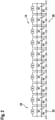
- Fig. 2 shows a circuit diagram for one of the phase branches 18 of the rectifier 16.
- the phase branch 18 comprises a plurality (for example more than 5) series-connected semiconductor devices 22 (here diodes).
- the semiconductor devices may be transistors or thyristors.
- Each semiconductor device 22 is part of a cell 24, which besides the semiconductor devices 22 comprises a varistor V, a resistor R1 and a series-connection of a resistor R2 and a capacitor C connected in parallel.
- These components of the phase branch 18 form a passive balancing and protection network of the phase branch 18. It is possible that solely the resistor R1, solely the series-connection of the resistor R2 and the capacitor or solely the varistor V is present. Also combinations of these components are possible.
- phase branch 18 may process currents between about 50 to 100 A.
- every phase branch 18 as shown in Fig. 2 is provided by a semiconductor module 26, examples of which will be described with respect to Fig. 4 to 8 .
- Fig. 3 shows a schematic perspective layout of an inverter 16 composed of 18 phase branches 18 provided by 18 semiconductor modules 26.
- an inverter 16 composed of semiconductor modules 26 with semiconductor devices 22 is described.
- the semiconductor devices 22 may be diodes and the inverter 16 may be a rectifier. It also is possible that the semiconductor devices 22 are active semiconductor switches and that the inverter 16 can be actively controlled.
- each semiconductor module 26 has an orientation or forward direction, which is aligned in parallel or antiparallel to a length direction L of the semiconductor modules 26 and the inverter 16.
- Three of the semiconductor modules 26 are stacked with each other in a height direction H. These semiconductor modules 26 are connected on one side to an AC phase input A1, B1, C1 or A2, B2, C2 or A3, B3, C3 and on another side to the DC+ input or DC- input.
- the stacked semiconductor modules 26 are all oriented in the same direction and are all connected to the same DC input, DC+, DC-.
- the orientation in the width direction W is alternating.
- Half of the semiconductor modules 26 are row-wise mounted in opposing directions.
- the orientation of a semiconductor module 26 may be enforced by dedicated plugs at the back of slots, where the semiconductor modules 26 are inserted as will be explained with respect to Fig. 9-11 . Also special grooves may enforce the orientation.
- the arrow 28 depicts a mounting movement of the semiconductor module 26 into the slots along the length direction L.
- the semiconductor modules 26 have special openings and specially aligned heat sinks to allow an air flow 30 through the inverter 16 along the height direction H (substantially parallel or antiparallel to the height direction H).
- the air flow 30 is substantially orthogonal to a current flow, which is substantially in parallel (or antiparallel) to the length direction L.
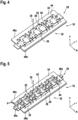
- Fig. 4-7 show a semiconductor module 26, which provides one of the phase legs 18, in different assembly stages.
- Fig. 4 shows a carrier plate 32 of a semiconductor module 26, which comprises a support frame 34 and a printed circuit board 36, which is attached on top of the support frame 34.
- the attachment may be done with screws, bolts or glue.
- the support frame 34 may be made of an electrically insulating material. This may guarantee the required insulation distance. Openings 38 in the support frame 34, which are surrounded by the material of the support frame 34 and openings 40 in the border of the printed circuit board 36, which overlap each other, generate openings 42 in the support frame 34, which allow an air flow 30 through the support frame 34 in height direction H.
- the support frame 34 also has protrusions 44 for supporting heat sinks.
- Fig. 4 also shows that edges 46a, 46b of the support frame 34, which run in parallel to the length direction, have a different cross-section.
- Edge 46a has a rectangular cross-section
- edge 46b has a triangular cross-section. This is used for enforcing an orientation of the semiconductor module 26 in the inverter 16.
- Fig. 5 shows the semiconductor module 26 with varistors V and semiconductor devices 22 mounted to the printed circuit board 36.
- the components V, 22 all protrude in the height direction from the printed circuit board 36. From a view direction in height direction, the components V, 22 do not overlap the openings 42 in the carrier plate 32.
- two connectors 48a, 48b are mounted to ends of the printed circuit board 36.
- the connectors 48a, 48b are of different type so as to enforce an orientation of the semiconductor module 26 in the inverter 16, when connected to a corresponding plug.
- Fig. 6 shows additionally that heat sinks 50 are mounted to the carrier plate 32.
- the fins 52 of the heat sinks are aligned in parallel to the height direction H and in parallel to the air flow direction 30, which is substantially orthogonal to the current flow 54 in length direction.
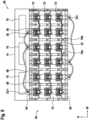
- Fig. 7 shows a top view in height direction onto the semiconductor module 26 as shown in Fig. 6 .
- the heat sinks 50 have a cooling interface 56, which is aligned orthogonal to the length direction L and to which two semiconductor devices 22 are connected.
- the two semiconductor devices 22 of a cell 24 are arranged in a row along the width directions W. The same applies to the varistors V.
- Every heat sink 50 is U-shaped, wherein the legs of the U and the fins 52 connected thereto are protruding beyond the border of the printed circuit board 36 and protrude over the opening 38, 42.
- the fins 52 connected to the bottom of the U are situated above the opening 40, 42.
- Fig. 8 shows a top view of further embodiments of a semiconductor module 26.
- the printed circuit board 36 does not have air flow openings but is substantially rectangular. Solely the support frame 34 provides openings 38, 42.
- the semiconductor devices 22 are aligned in two rows along edges of the printed circuit board 36 in length direction L.
- the heat sinks 50 have a cooling interface 56, which is aligned orthogonal to the width direction W and to which two semiconductor devices 22 are connected. There are two heat sinks 50 per cell 24.
- every heat sink 50 is comb-shaped, wherein the fins 52, which are aligned orthogonal to the length direction L, are protruding beyond the border of the printed circuit board 36 and protrude over the opening 38, 42.
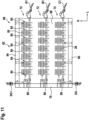
- Fig. 9 , 10 and 11 show a converter assembly 60 in a cross-sectional front view, top view and side view.
- the converter assembly 60 comprises an assembly box 62 made of a horizontal top wall 64, a horizontal bottom wall 66, a back wall 70 and vertical walls 68.
- the assembly box 62 and in particular the walls 64, 66, 68 are made of an insulating material. As shown, the walls 64, 66, 68 may be interconnected by screwing. However, also other types of interconnections like bolts are possible.
- the horizontal top wall 64 and the horizontal bottom wall 66 are orthogonal to the height direction H.
- the vertical walls 68 are orthogonal to the width direction W.
- the back wall 70 is orthogonal to the length direction L.
- slots 72 for receiving semiconductor modules 26 are formed inside the assembly box 62. In each slot 72, one semiconductor module 26 is accommodated.
- the semiconductor modules 26 are designed such as shown in Fig. 6 and 7 . However, also other semiconductor modules 26, for example such as shown in Fig. 8 , may be used.
- the inverter formed from the semiconductor modules 26 is like the one shown in Fig. 1 and 3 .
- the 18 semiconductor modules 26 in the assembly box 62 are electrically interconnected to form an 18-pulse inverter.
- each semiconductor module 26 may comprise 7 cells, such as shown in Fig. 6 to 8 . However, other numbers of cells are possible.
- the semiconductor modules 26 are electrically interconnected with a DC+ output and a DC- output and at the front side, the semiconductor modules 26 are electrically interconnected with AC inputs A1, A2, A3, B1, B2, B3, C1, C2, C3, such as shown in Fig. 3 .
- Other dimensions are possible.
- Fig. 9 additionally shows schematically a top box 74 with fans 76, the fans 76 generating an air flow in parallel or antiparallel to the height direction H.
- the airflow passes through the semiconductor modules 26 and in particular through the heat sinks 50 of the semiconductor modules 26. Due to the openings 38 (see Fig. 6-8 ) in the support frames 34 of the semiconductor modules 26 and the alignment of the fins 52, the air flow can pass directly through the semiconductor modules 26.
- the semiconductor modules 26 have different orientations in the slots 72, either their length direction is aligned parallel to the length direction L of the assembly box 62 or their length direction is aligned anti-parallel to the length direction L of the assembly box 62. This is also shown in Fig. 3 .
- the parallel aligned semiconductor modules 26 provide the upper branches of the inverter, which the anti-parallel aligned semiconductor modules 26 provide the lower branches.
- the semiconductor modules 26 are designed exchangeable and there are grooves 78a, 78b provided in the vertical walls 68 for inserting the semiconductor modules 26 in a simple way.
- the grooves 78a, 78b of one slot 72 are designed to receive the edges 46a, 46b of the carrier plate 32 of the respective semiconductor module 26.
- the grooves 78a have a rectangular cross-section, while the grooves 78b have a triangular cross-section.
- First semiconductor modules 26 are aligned in first slots 72 such that their length directions L point towards the back wall 70 of the assembly box 62 and second semiconductor modules 26 are aligned in second slots 72 such that their length directions L point away from the back wall 70.
- plugs 80 are arranged at back wall 70.
- First plugs 80 for receiving a first type of connector 48a of the semiconductor modules 26 are provided at the back wall 70 in the first slots 72 and second plugs 80, designed differently to the first plugs 80, for receiving a second type of connector 48a are provided at the back wall 70 in the second slots 72.
- the assembly box 62 has openings 82 in the top wall 64 and in the bottom wall 66, such that a cooling air flow in height direction H can pass through the semiconductor modules 26.
- the fans 76 may be arranged above these openings 82.
- the vertical walls 68 comprise openings 84, such that a cooling air flow in width direction W can leave the assembly box 62.
Landscapes
- Engineering & Computer Science (AREA)
- Microelectronics & Electronic Packaging (AREA)
- Physics & Mathematics (AREA)
- Thermal Sciences (AREA)
- Rectifiers (AREA)
Priority Applications (1)
| Application Number | Priority Date | Filing Date | Title |
|---|---|---|---|
| EP21214518.9A EP4199664B1 (de) | 2021-12-14 | 2021-12-14 | Mehrmodulwandler mit verbesserter kühlung |
Applications Claiming Priority (1)
| Application Number | Priority Date | Filing Date | Title |
|---|---|---|---|
| EP21214518.9A EP4199664B1 (de) | 2021-12-14 | 2021-12-14 | Mehrmodulwandler mit verbesserter kühlung |
Publications (3)
| Publication Number | Publication Date |
|---|---|
| EP4199664A1 true EP4199664A1 (de) | 2023-06-21 |
| EP4199664B1 EP4199664B1 (de) | 2026-02-11 |
| EP4199664C0 EP4199664C0 (de) | 2026-02-11 |
Family
ID=78916820
Family Applications (1)
| Application Number | Title | Priority Date | Filing Date |
|---|---|---|---|
| EP21214518.9A Active EP4199664B1 (de) | 2021-12-14 | 2021-12-14 | Mehrmodulwandler mit verbesserter kühlung |
Country Status (1)
| Country | Link |
|---|---|
| EP (1) | EP4199664B1 (de) |
Citations (6)
| Publication number | Priority date | Publication date | Assignee | Title |
|---|---|---|---|---|
| US3573574A (en) * | 1969-08-12 | 1971-04-06 | Gen Motors Corp | Controlled rectifier mounting assembly |
| US3646400A (en) * | 1970-12-21 | 1972-02-29 | Gen Electric | Air-cooling system for hvdc valve with staggered rectifiers |
| US3697814A (en) * | 1971-06-21 | 1972-10-10 | Gen Motors Corp | Bridge rectifier heat sink assembly |
| DE2718967A1 (de) * | 1976-03-17 | 1978-11-09 | Siemens Ag | Stromrichterbaueinheit |
| US6262906B1 (en) * | 1996-05-21 | 2001-07-17 | Siemens Aktiengesellschaft | Air-cooled power converter, drive device for rolling stands, and power converter system |
| US20140374394A1 (en) * | 2013-06-24 | 2014-12-25 | Illinois Tool Works Inc. | Integrated electrical components of a welding power supply |
-
2021
- 2021-12-14 EP EP21214518.9A patent/EP4199664B1/de active Active
Patent Citations (6)
| Publication number | Priority date | Publication date | Assignee | Title |
|---|---|---|---|---|
| US3573574A (en) * | 1969-08-12 | 1971-04-06 | Gen Motors Corp | Controlled rectifier mounting assembly |
| US3646400A (en) * | 1970-12-21 | 1972-02-29 | Gen Electric | Air-cooling system for hvdc valve with staggered rectifiers |
| US3697814A (en) * | 1971-06-21 | 1972-10-10 | Gen Motors Corp | Bridge rectifier heat sink assembly |
| DE2718967A1 (de) * | 1976-03-17 | 1978-11-09 | Siemens Ag | Stromrichterbaueinheit |
| US6262906B1 (en) * | 1996-05-21 | 2001-07-17 | Siemens Aktiengesellschaft | Air-cooled power converter, drive device for rolling stands, and power converter system |
| US20140374394A1 (en) * | 2013-06-24 | 2014-12-25 | Illinois Tool Works Inc. | Integrated electrical components of a welding power supply |
Also Published As
| Publication number | Publication date |
|---|---|
| EP4199664B1 (de) | 2026-02-11 |
| EP4199664C0 (de) | 2026-02-11 |
Similar Documents
| Publication | Publication Date | Title |
|---|---|---|
| US8004836B2 (en) | Arrangement for a motor controller | |
| EP2277365B1 (de) | Mit einer verdampfbaren dielektrischen füssigkeit gekühlter modularer hochleistungsantriebsblock | |
| US9270199B2 (en) | Power conversion apparatus with a laminated bus bar comprising an exposed heat radiating portion | |
| US7443692B2 (en) | Power converter architecture employing at least one capacitor across a DC bus | |
| CN103477549B (zh) | 两件式变流器单元 | |
| US7830111B2 (en) | Power delivery system including interchangeable cells | |
| JP3300566B2 (ja) | パワーモジュール及び電力変換装置 | |
| CN102714494A (zh) | 发电装置的断路器的电路布置 | |
| US20130320896A1 (en) | Modular inverter arrangement | |
| CN105429443A (zh) | 具有多相的变流器的变流器布置 | |
| KR102531831B1 (ko) | 전력 변환 유닛 | |
| KR20180052707A (ko) | 절연을 갖는 인쇄 회로 기판 전력 셀 및 중간 전압 다중-셀 전력 공급부 | |
| CN113994559B (zh) | 层压母排、电力变换器、电力变换装置及不间断电源装置 | |
| EP3528605B1 (de) | Kompakte bauweise von mehrstufigen stromrichtersystemen | |
| EP4199664B1 (de) | Mehrmodulwandler mit verbesserter kühlung | |
| JP2022145741A (ja) | 無停電電源装置用制御装置 | |
| JP2015115523A (ja) | 電力変換装置用半導体装置および電力変換装置 | |
| WO2018177732A1 (en) | 3-level power module | |
| CN207150437U (zh) | 用于将dc电力转换为三相ac电力的转换系统以及包括该转换系统的电动机系统 | |
| JP7771523B2 (ja) | 電力変換装置 | |
| KR100833569B1 (ko) | 대용량 전력변환기용 균등분배 병렬구조의 igbt스택장치 | |
| US20210328522A1 (en) | Rectifier assembly | |
| JP7841628B2 (ja) | 電力変換装置 | |
| CN205755209U (zh) | 电力电子器件 | |
| KR102877586B1 (ko) | 전력 변환 장치 |
Legal Events
| Date | Code | Title | Description |
|---|---|---|---|
| PUAI | Public reference made under article 153(3) epc to a published international application that has entered the european phase |
Free format text: ORIGINAL CODE: 0009012 |
|
| STAA | Information on the status of an ep patent application or granted ep patent |
Free format text: STATUS: THE APPLICATION HAS BEEN PUBLISHED |
|
| AK | Designated contracting states |
Kind code of ref document: A1 Designated state(s): AL AT BE BG CH CY CZ DE DK EE ES FI FR GB GR HR HU IE IS IT LI LT LU LV MC MK MT NL NO PL PT RO RS SE SI SK SM TR |
|
| STAA | Information on the status of an ep patent application or granted ep patent |
Free format text: STATUS: REQUEST FOR EXAMINATION WAS MADE |
|
| 17P | Request for examination filed |
Effective date: 20231218 |
|
| RBV | Designated contracting states (corrected) |
Designated state(s): AL AT BE BG CH CY CZ DE DK EE ES FI FR GB GR HR HU IE IS IT LI LT LU LV MC MK MT NL NO PL PT RO RS SE SI SK SM TR |
|
| GRAP | Despatch of communication of intention to grant a patent |
Free format text: ORIGINAL CODE: EPIDOSNIGR1 |
|
| STAA | Information on the status of an ep patent application or granted ep patent |
Free format text: STATUS: GRANT OF PATENT IS INTENDED |
|
| INTG | Intention to grant announced |
Effective date: 20250919 |
|
| GRAS | Grant fee paid |
Free format text: ORIGINAL CODE: EPIDOSNIGR3 |
|
| GRAA | (expected) grant |
Free format text: ORIGINAL CODE: 0009210 |
|
| STAA | Information on the status of an ep patent application or granted ep patent |
Free format text: STATUS: THE PATENT HAS BEEN GRANTED |
|
| AK | Designated contracting states |
Kind code of ref document: B1 Designated state(s): AL AT BE BG CH CY CZ DE DK EE ES FI FR GB GR HR HU IE IS IT LI LT LU LV MC MK MT NL NO PL PT RO RS SE SI SK SM TR |
|
| REG | Reference to a national code |
Ref country code: CH Ref legal event code: F10 Free format text: ST27 STATUS EVENT CODE: U-0-0-F10-F00 (AS PROVIDED BY THE NATIONAL OFFICE) Effective date: 20260211 Ref country code: GB Ref legal event code: FG4D |
|
| REG | Reference to a national code |
Ref country code: DE Ref legal event code: R096 Ref document number: 602021047647 Country of ref document: DE |
|
| REG | Reference to a national code |
Ref country code: IE Ref legal event code: FG4D |
|
| U01 | Request for unitary effect filed |
Effective date: 20260304 |
|
| U07 | Unitary effect registered |
Designated state(s): AT BE BG DE DK EE FI FR IT LT LU LV MT NL PT RO SE SI Effective date: 20260310 |