EP4200462B1 - Fenêtre pour systèmes de dépôt chimique en phase vapeur et procédés associés - Google Patents
Fenêtre pour systèmes de dépôt chimique en phase vapeur et procédés associés Download PDFInfo
- Publication number
- EP4200462B1 EP4200462B1 EP21766306.1A EP21766306A EP4200462B1 EP 4200462 B1 EP4200462 B1 EP 4200462B1 EP 21766306 A EP21766306 A EP 21766306A EP 4200462 B1 EP4200462 B1 EP 4200462B1
- Authority
- EP
- European Patent Office
- Prior art keywords
- substrate
- curvature
- radius
- window
- gas
- Prior art date
- Legal status (The legal status is an assumption and is not a legal conclusion. Google has not performed a legal analysis and makes no representation as to the accuracy of the status listed.)
- Active
Links
Images



Classifications
-
- C—CHEMISTRY; METALLURGY
- C23—COATING METALLIC MATERIAL; COATING MATERIAL WITH METALLIC MATERIAL; CHEMICAL SURFACE TREATMENT; DIFFUSION TREATMENT OF METALLIC MATERIAL; COATING BY VACUUM EVAPORATION, BY SPUTTERING, BY ION IMPLANTATION OR BY CHEMICAL VAPOUR DEPOSITION, IN GENERAL; INHIBITING CORROSION OF METALLIC MATERIAL OR INCRUSTATION IN GENERAL
- C23C—COATING METALLIC MATERIAL; COATING MATERIAL WITH METALLIC MATERIAL; SURFACE TREATMENT OF METALLIC MATERIAL BY DIFFUSION INTO THE SURFACE, BY CHEMICAL CONVERSION OR SUBSTITUTION; COATING BY VACUUM EVAPORATION, BY SPUTTERING, BY ION IMPLANTATION OR BY CHEMICAL VAPOUR DEPOSITION, IN GENERAL
- C23C16/00—Chemical coating by decomposition of gaseous compounds, without leaving reaction products of surface material in the coating, i.e. chemical vapour deposition [CVD] processes
- C23C16/44—Chemical coating by decomposition of gaseous compounds, without leaving reaction products of surface material in the coating, i.e. chemical vapour deposition [CVD] processes characterised by the method of coating
- C23C16/455—Chemical coating by decomposition of gaseous compounds, without leaving reaction products of surface material in the coating, i.e. chemical vapour deposition [CVD] processes characterised by the method of coating characterised by the method used for introducing gases into reaction chamber or for modifying gas flows in reaction chamber
- C23C16/45502—Flow conditions in reaction chamber
-
- C—CHEMISTRY; METALLURGY
- C23—COATING METALLIC MATERIAL; COATING MATERIAL WITH METALLIC MATERIAL; CHEMICAL SURFACE TREATMENT; DIFFUSION TREATMENT OF METALLIC MATERIAL; COATING BY VACUUM EVAPORATION, BY SPUTTERING, BY ION IMPLANTATION OR BY CHEMICAL VAPOUR DEPOSITION, IN GENERAL; INHIBITING CORROSION OF METALLIC MATERIAL OR INCRUSTATION IN GENERAL
- C23C—COATING METALLIC MATERIAL; COATING MATERIAL WITH METALLIC MATERIAL; SURFACE TREATMENT OF METALLIC MATERIAL BY DIFFUSION INTO THE SURFACE, BY CHEMICAL CONVERSION OR SUBSTITUTION; COATING BY VACUUM EVAPORATION, BY SPUTTERING, BY ION IMPLANTATION OR BY CHEMICAL VAPOUR DEPOSITION, IN GENERAL
- C23C16/00—Chemical coating by decomposition of gaseous compounds, without leaving reaction products of surface material in the coating, i.e. chemical vapour deposition [CVD] processes
- C23C16/44—Chemical coating by decomposition of gaseous compounds, without leaving reaction products of surface material in the coating, i.e. chemical vapour deposition [CVD] processes characterised by the method of coating
- C23C16/455—Chemical coating by decomposition of gaseous compounds, without leaving reaction products of surface material in the coating, i.e. chemical vapour deposition [CVD] processes characterised by the method of coating characterised by the method used for introducing gases into reaction chamber or for modifying gas flows in reaction chamber
- C23C16/45502—Flow conditions in reaction chamber
- C23C16/45504—Laminar flow
-
- C—CHEMISTRY; METALLURGY
- C23—COATING METALLIC MATERIAL; COATING MATERIAL WITH METALLIC MATERIAL; CHEMICAL SURFACE TREATMENT; DIFFUSION TREATMENT OF METALLIC MATERIAL; COATING BY VACUUM EVAPORATION, BY SPUTTERING, BY ION IMPLANTATION OR BY CHEMICAL VAPOUR DEPOSITION, IN GENERAL; INHIBITING CORROSION OF METALLIC MATERIAL OR INCRUSTATION IN GENERAL
- C23C—COATING METALLIC MATERIAL; COATING MATERIAL WITH METALLIC MATERIAL; SURFACE TREATMENT OF METALLIC MATERIAL BY DIFFUSION INTO THE SURFACE, BY CHEMICAL CONVERSION OR SUBSTITUTION; COATING BY VACUUM EVAPORATION, BY SPUTTERING, BY ION IMPLANTATION OR BY CHEMICAL VAPOUR DEPOSITION, IN GENERAL
- C23C16/00—Chemical coating by decomposition of gaseous compounds, without leaving reaction products of surface material in the coating, i.e. chemical vapour deposition [CVD] processes
- C23C16/44—Chemical coating by decomposition of gaseous compounds, without leaving reaction products of surface material in the coating, i.e. chemical vapour deposition [CVD] processes characterised by the method of coating
- C23C16/455—Chemical coating by decomposition of gaseous compounds, without leaving reaction products of surface material in the coating, i.e. chemical vapour deposition [CVD] processes characterised by the method of coating characterised by the method used for introducing gases into reaction chamber or for modifying gas flows in reaction chamber
- C23C16/45517—Confinement of gases to vicinity of substrate
-
- C—CHEMISTRY; METALLURGY
- C23—COATING METALLIC MATERIAL; COATING MATERIAL WITH METALLIC MATERIAL; CHEMICAL SURFACE TREATMENT; DIFFUSION TREATMENT OF METALLIC MATERIAL; COATING BY VACUUM EVAPORATION, BY SPUTTERING, BY ION IMPLANTATION OR BY CHEMICAL VAPOUR DEPOSITION, IN GENERAL; INHIBITING CORROSION OF METALLIC MATERIAL OR INCRUSTATION IN GENERAL
- C23C—COATING METALLIC MATERIAL; COATING MATERIAL WITH METALLIC MATERIAL; SURFACE TREATMENT OF METALLIC MATERIAL BY DIFFUSION INTO THE SURFACE, BY CHEMICAL CONVERSION OR SUBSTITUTION; COATING BY VACUUM EVAPORATION, BY SPUTTERING, BY ION IMPLANTATION OR BY CHEMICAL VAPOUR DEPOSITION, IN GENERAL
- C23C16/00—Chemical coating by decomposition of gaseous compounds, without leaving reaction products of surface material in the coating, i.e. chemical vapour deposition [CVD] processes
- C23C16/44—Chemical coating by decomposition of gaseous compounds, without leaving reaction products of surface material in the coating, i.e. chemical vapour deposition [CVD] processes characterised by the method of coating
- C23C16/455—Chemical coating by decomposition of gaseous compounds, without leaving reaction products of surface material in the coating, i.e. chemical vapour deposition [CVD] processes characterised by the method of coating characterised by the method used for introducing gases into reaction chamber or for modifying gas flows in reaction chamber
- C23C16/45585—Compression of gas before it reaches the substrate
-
- C—CHEMISTRY; METALLURGY
- C23—COATING METALLIC MATERIAL; COATING MATERIAL WITH METALLIC MATERIAL; CHEMICAL SURFACE TREATMENT; DIFFUSION TREATMENT OF METALLIC MATERIAL; COATING BY VACUUM EVAPORATION, BY SPUTTERING, BY ION IMPLANTATION OR BY CHEMICAL VAPOUR DEPOSITION, IN GENERAL; INHIBITING CORROSION OF METALLIC MATERIAL OR INCRUSTATION IN GENERAL
- C23C—COATING METALLIC MATERIAL; COATING MATERIAL WITH METALLIC MATERIAL; SURFACE TREATMENT OF METALLIC MATERIAL BY DIFFUSION INTO THE SURFACE, BY CHEMICAL CONVERSION OR SUBSTITUTION; COATING BY VACUUM EVAPORATION, BY SPUTTERING, BY ION IMPLANTATION OR BY CHEMICAL VAPOUR DEPOSITION, IN GENERAL
- C23C16/00—Chemical coating by decomposition of gaseous compounds, without leaving reaction products of surface material in the coating, i.e. chemical vapour deposition [CVD] processes
- C23C16/44—Chemical coating by decomposition of gaseous compounds, without leaving reaction products of surface material in the coating, i.e. chemical vapour deposition [CVD] processes characterised by the method of coating
- C23C16/455—Chemical coating by decomposition of gaseous compounds, without leaving reaction products of surface material in the coating, i.e. chemical vapour deposition [CVD] processes characterised by the method of coating characterised by the method used for introducing gases into reaction chamber or for modifying gas flows in reaction chamber
- C23C16/45587—Mechanical means for changing the gas flow
- C23C16/45591—Fixed means, e.g. wings, baffles
-
- C—CHEMISTRY; METALLURGY
- C23—COATING METALLIC MATERIAL; COATING MATERIAL WITH METALLIC MATERIAL; CHEMICAL SURFACE TREATMENT; DIFFUSION TREATMENT OF METALLIC MATERIAL; COATING BY VACUUM EVAPORATION, BY SPUTTERING, BY ION IMPLANTATION OR BY CHEMICAL VAPOUR DEPOSITION, IN GENERAL; INHIBITING CORROSION OF METALLIC MATERIAL OR INCRUSTATION IN GENERAL
- C23C—COATING METALLIC MATERIAL; COATING MATERIAL WITH METALLIC MATERIAL; SURFACE TREATMENT OF METALLIC MATERIAL BY DIFFUSION INTO THE SURFACE, BY CHEMICAL CONVERSION OR SUBSTITUTION; COATING BY VACUUM EVAPORATION, BY SPUTTERING, BY ION IMPLANTATION OR BY CHEMICAL VAPOUR DEPOSITION, IN GENERAL
- C23C16/00—Chemical coating by decomposition of gaseous compounds, without leaving reaction products of surface material in the coating, i.e. chemical vapour deposition [CVD] processes
- C23C16/44—Chemical coating by decomposition of gaseous compounds, without leaving reaction products of surface material in the coating, i.e. chemical vapour deposition [CVD] processes characterised by the method of coating
- C23C16/458—Chemical coating by decomposition of gaseous compounds, without leaving reaction products of surface material in the coating, i.e. chemical vapour deposition [CVD] processes characterised by the method of coating characterised by the method used for supporting substrates in the reaction chamber
-
- C—CHEMISTRY; METALLURGY
- C23—COATING METALLIC MATERIAL; COATING MATERIAL WITH METALLIC MATERIAL; CHEMICAL SURFACE TREATMENT; DIFFUSION TREATMENT OF METALLIC MATERIAL; COATING BY VACUUM EVAPORATION, BY SPUTTERING, BY ION IMPLANTATION OR BY CHEMICAL VAPOUR DEPOSITION, IN GENERAL; INHIBITING CORROSION OF METALLIC MATERIAL OR INCRUSTATION IN GENERAL
- C23C—COATING METALLIC MATERIAL; COATING MATERIAL WITH METALLIC MATERIAL; SURFACE TREATMENT OF METALLIC MATERIAL BY DIFFUSION INTO THE SURFACE, BY CHEMICAL CONVERSION OR SUBSTITUTION; COATING BY VACUUM EVAPORATION, BY SPUTTERING, BY ION IMPLANTATION OR BY CHEMICAL VAPOUR DEPOSITION, IN GENERAL
- C23C16/00—Chemical coating by decomposition of gaseous compounds, without leaving reaction products of surface material in the coating, i.e. chemical vapour deposition [CVD] processes
- C23C16/44—Chemical coating by decomposition of gaseous compounds, without leaving reaction products of surface material in the coating, i.e. chemical vapour deposition [CVD] processes characterised by the method of coating
- C23C16/48—Chemical coating by decomposition of gaseous compounds, without leaving reaction products of surface material in the coating, i.e. chemical vapour deposition [CVD] processes characterised by the method of coating by irradiation, e.g. photolysis, radiolysis, particle radiation
- C23C16/481—Chemical coating by decomposition of gaseous compounds, without leaving reaction products of surface material in the coating, i.e. chemical vapour deposition [CVD] processes characterised by the method of coating by irradiation, e.g. photolysis, radiolysis, particle radiation by radiant heating of the substrate
-
- C—CHEMISTRY; METALLURGY
- C23—COATING METALLIC MATERIAL; COATING MATERIAL WITH METALLIC MATERIAL; CHEMICAL SURFACE TREATMENT; DIFFUSION TREATMENT OF METALLIC MATERIAL; COATING BY VACUUM EVAPORATION, BY SPUTTERING, BY ION IMPLANTATION OR BY CHEMICAL VAPOUR DEPOSITION, IN GENERAL; INHIBITING CORROSION OF METALLIC MATERIAL OR INCRUSTATION IN GENERAL
- C23C—COATING METALLIC MATERIAL; COATING MATERIAL WITH METALLIC MATERIAL; SURFACE TREATMENT OF METALLIC MATERIAL BY DIFFUSION INTO THE SURFACE, BY CHEMICAL CONVERSION OR SUBSTITUTION; COATING BY VACUUM EVAPORATION, BY SPUTTERING, BY ION IMPLANTATION OR BY CHEMICAL VAPOUR DEPOSITION, IN GENERAL
- C23C16/00—Chemical coating by decomposition of gaseous compounds, without leaving reaction products of surface material in the coating, i.e. chemical vapour deposition [CVD] processes
- C23C16/44—Chemical coating by decomposition of gaseous compounds, without leaving reaction products of surface material in the coating, i.e. chemical vapour deposition [CVD] processes characterised by the method of coating
- C23C16/48—Chemical coating by decomposition of gaseous compounds, without leaving reaction products of surface material in the coating, i.e. chemical vapour deposition [CVD] processes characterised by the method of coating by irradiation, e.g. photolysis, radiolysis, particle radiation
- C23C16/482—Chemical coating by decomposition of gaseous compounds, without leaving reaction products of surface material in the coating, i.e. chemical vapour deposition [CVD] processes characterised by the method of coating by irradiation, e.g. photolysis, radiolysis, particle radiation using incoherent light, UV to IR, e.g. lamps
-
- C—CHEMISTRY; METALLURGY
- C23—COATING METALLIC MATERIAL; COATING MATERIAL WITH METALLIC MATERIAL; CHEMICAL SURFACE TREATMENT; DIFFUSION TREATMENT OF METALLIC MATERIAL; COATING BY VACUUM EVAPORATION, BY SPUTTERING, BY ION IMPLANTATION OR BY CHEMICAL VAPOUR DEPOSITION, IN GENERAL; INHIBITING CORROSION OF METALLIC MATERIAL OR INCRUSTATION IN GENERAL
- C23C—COATING METALLIC MATERIAL; COATING MATERIAL WITH METALLIC MATERIAL; SURFACE TREATMENT OF METALLIC MATERIAL BY DIFFUSION INTO THE SURFACE, BY CHEMICAL CONVERSION OR SUBSTITUTION; COATING BY VACUUM EVAPORATION, BY SPUTTERING, BY ION IMPLANTATION OR BY CHEMICAL VAPOUR DEPOSITION, IN GENERAL
- C23C16/00—Chemical coating by decomposition of gaseous compounds, without leaving reaction products of surface material in the coating, i.e. chemical vapour deposition [CVD] processes
- C23C16/44—Chemical coating by decomposition of gaseous compounds, without leaving reaction products of surface material in the coating, i.e. chemical vapour deposition [CVD] processes characterised by the method of coating
- C23C16/48—Chemical coating by decomposition of gaseous compounds, without leaving reaction products of surface material in the coating, i.e. chemical vapour deposition [CVD] processes characterised by the method of coating by irradiation, e.g. photolysis, radiolysis, particle radiation
- C23C16/488—Protection of windows for introduction of radiation into the coating chamber
-
- C—CHEMISTRY; METALLURGY
- C23—COATING METALLIC MATERIAL; COATING MATERIAL WITH METALLIC MATERIAL; CHEMICAL SURFACE TREATMENT; DIFFUSION TREATMENT OF METALLIC MATERIAL; COATING BY VACUUM EVAPORATION, BY SPUTTERING, BY ION IMPLANTATION OR BY CHEMICAL VAPOUR DEPOSITION, IN GENERAL; INHIBITING CORROSION OF METALLIC MATERIAL OR INCRUSTATION IN GENERAL
- C23C—COATING METALLIC MATERIAL; COATING MATERIAL WITH METALLIC MATERIAL; SURFACE TREATMENT OF METALLIC MATERIAL BY DIFFUSION INTO THE SURFACE, BY CHEMICAL CONVERSION OR SUBSTITUTION; COATING BY VACUUM EVAPORATION, BY SPUTTERING, BY ION IMPLANTATION OR BY CHEMICAL VAPOUR DEPOSITION, IN GENERAL
- C23C16/00—Chemical coating by decomposition of gaseous compounds, without leaving reaction products of surface material in the coating, i.e. chemical vapour deposition [CVD] processes
- C23C16/44—Chemical coating by decomposition of gaseous compounds, without leaving reaction products of surface material in the coating, i.e. chemical vapour deposition [CVD] processes characterised by the method of coating
- C23C16/52—Controlling or regulating the coating process
-
- H—ELECTRICITY
- H10—SEMICONDUCTOR DEVICES; ELECTRIC SOLID-STATE DEVICES NOT OTHERWISE PROVIDED FOR
- H10P—GENERIC PROCESSES OR APPARATUS FOR THE MANUFACTURE OR TREATMENT OF DEVICES COVERED BY CLASS H10
- H10P14/00—Formation of materials, e.g. in the shape of layers or pillars
- H10P14/60—Formation of materials, e.g. in the shape of layers or pillars of insulating materials
- H10P14/63—Formation of materials, e.g. in the shape of layers or pillars of insulating materials characterised by the formation processes
- H10P14/6326—Deposition processes
- H10P14/6349—Deposition of epitaxial materials
-
- C—CHEMISTRY; METALLURGY
- C30—CRYSTAL GROWTH
- C30B—SINGLE-CRYSTAL GROWTH; UNIDIRECTIONAL SOLIDIFICATION OF EUTECTIC MATERIAL OR UNIDIRECTIONAL DEMIXING OF EUTECTOID MATERIAL; REFINING BY ZONE-MELTING OF MATERIAL; PRODUCTION OF A HOMOGENEOUS POLYCRYSTALLINE MATERIAL WITH DEFINED STRUCTURE; SINGLE CRYSTALS OR HOMOGENEOUS POLYCRYSTALLINE MATERIAL WITH DEFINED STRUCTURE; AFTER-TREATMENT OF SINGLE CRYSTALS OR A HOMOGENEOUS POLYCRYSTALLINE MATERIAL WITH DEFINED STRUCTURE; APPARATUS THEREFOR
- C30B25/00—Single-crystal growth by chemical reaction of reactive gases, e.g. chemical vapour-deposition growth
- C30B25/02—Epitaxial-layer growth
- C30B25/16—Controlling or regulating
- C30B25/165—Controlling or regulating the flow of the reactive gases
Definitions
- the field relates generally to the use of chemical vapor deposition systems in processing semiconductor wafers and, more specifically, to windows and to methods for controlling the uniformity of gas flow within a chemical vapor deposition process chamber.
- uniformity in the thickness of a deposited film on a substrate is dependent on, among other factors, uniformity in the flow distribution of gasses within the process chamber. As the requirements for uniformity in film thickness become more stringent, the desire for more uniform flow rate distribution of gasses in the process chamber increases.
- a source gas is introduced into the process chamber through a gas manifold and is directed between a gap defined between an upper window of the process chamber and a substrate positioned on a substrate support.
- the upper windows of conventional CVD devices do not direct a uniform gas flow distribution across the substrate surface in the processing chamber.
- some conventional upper windows include a curved surface spanning the process chamber and facing the substrate that may be convex, dipping towards the center of the substrate.
- such conventional upper windows may produce a turbulent gas flow about the substrate resulting in dips or depressions in the epitaxy deposited on the substrate.
- some conventional CVD systems attempt to minimize the depth of the dips in the epitaxy thickness profile by operating at a decreased growth rate (e.g., at a lower deposition temperature within the processing chamber and/or at a reduced gas flow rate).
- a decreased growth rate e.g., at a lower deposition temperature within the processing chamber and/or at a reduced gas flow rate.
- such system of operation can result in longer process times with only moderate changes in the depth of the dips in the deposited epitaxy.
- US 2010/251958 A1 describes a single wafer processing epitaxial growth method by which a single crystal substrate is placed in a reaction chamber with an upper wall having a downward convexity and an epitaxial layer is deposited on the single crystal substrate by introducing raw material gas and carrier gas into the reaction chamber through a gas feed port, in which, after any one of the radius of curvature of the upper wall of the reaction chamber and a difference between an upper end of the gas feed port and a lower end of the upper wall of the reaction chamber in the height direction or both are adjusted in accordance with the flow rate of the carrier gas which is introduced into the reaction chamber through the gas feed port, an epitaxial layer is deposited on the single crystal substrate.
- US 6,869,485 B2 describes a semiconductor processing chamber wherein the inner surface of the window is substantially flat and parallel to the wafer to be processed.
- the window is thin in a center portion and thicker in a surrounding peripheral portion. The thickness increases in the radially outward direction, defined between the flat inner surface and a concave outer surface.
- the chamber employs multiple outlet ports for distributing gas laterally in a short length.
- One aspect of the present invention is directed to a system for depositing a layer on a substrate.
- the system includes a processing chamber defining a gas inlet for introducing gas into the processing chamber and a gas outlet to allow the gas to exit the processing chamber.
- a substrate support is positioned within the processing chamber and is configured to receive a substrate.
- a transparent upper window includes a convex first face spaced from the substrate support to define an air gap therebetween.
- the upper window is positioned within the processing chamber to direct the gas from the gas inlet, through the air gap, and to the gas outlet.
- the first face includes a radially outer surface and a radially inner surface circumscribed within the outer surface.
- the outer surface has a first radius of curvature and the inner surface has a second radius of curvature that is different from the first radius of curvature.
- the window includes a frame for attaching the window to a processing chamber of the substrate processing system and a transparent body connected to the frame.
- the body extends between a convex first face and an opposed second face.
- the first face includes a radially outer surface and a radially inner surface circumscribed within the outer surface.
- the outer surface extends radially from the frame to the inner surface and the inner surface extends radially inward from the outer surface to a radial center of the window.
- the outer surface has a first radius of curvature and the inner surface has a second radius of curvature that is different from the first radius of curvature.
- Yet another aspect of the present invention is directed to a method of depositing a layer on a substrate.
- the method includes providing a substrate on a substrate support within a processing chamber.
- the processing chamber includes a gas inlet and a gas outlet.
- the method further includes providing an upper window in the processing chamber.
- the upper window is transparent to enable radiant heating light to pass through the upper window.
- the upper window has a convex first face spaced from the substrate to define an air gap therebetween.
- the first face includes a radially outer surface and a radially inner surface circumscribed within the outer surface.
- the outer surface has a first radius of curvature and the inner surface has a second radius of curvature that is different from the first radius of curvature.
- the method further includes directing a gas flow through the gas inlet, into the air gap between the first face and the substrate, and to and to the gas outlet.
- a chemical vapor deposition (CVD) system also referred to herein as a "substrate processing system,” is indicated generally at 100 in Figure 1 .
- the illustrated system is a single substrate system, however, the system and methods disclosed herein for providing a more uniform gas flow distribution are suitable for use in other system designs including, for example, multiple substrate systems.
- One example of a CVD system suitable for use in accordance with the present invention is the Applied Materials EPI Centura 300.
- curvature refers to an amount by which a curve of a surface and/or a face deviates from a plane and the phrase "radius of curvature” refers to the radius of a circle and/or sphere whose perimeter has a curvature matching the curvature of the surface and/or face.
- a surface and/or face having a relatively large curvature includes a relatively high deviation from a plane at any point along the curve and a relatively short radius of curvature.
- a surface or face having a relatively small curvature will have a relatively low deviation from a plane at any point along the curve and a relatively large radius of curvature.
- the CVD system 100 includes a reaction or processing chamber 102 for depositing and/or growing thin films on a substrate 104 (e.g., a semiconductor wafer), a gas injection port 106 disposed at one end of the processing chamber 102, and a gas discharge port 108 disposed at an opposite end of the processing chamber 102.
- a gas manifold 140 disposed between the gas injecting port 106 and the processing chamber 102 is used to direct incoming gas 110 into the processing chamber 102 enclosed by an upper window 112 and a lower window 114 through the gas injection port 106.
- the gas manifold 140 includes an injector baffle or gas distribution plate disposed between the gas injecting port 106 and the processing chamber 102, and an inject insert liner assembly 170 disposed adjacent to the baffle plate and upstream from the processing chamber 102.
- an incoming process gas 110 flows through the gas manifold 140 and into the processing chamber 102 through gas inlet 103.
- the gas 110 then flows over the substrate surface 116 and reacts with the substrate surface 116, or precursors disposed thereon, to deposit a film on the substrate surface 116.
- the gas 110 then flows out of the processing chamber 102 and through the gas discharge port 108.
- the substrate 104 upon which the film is deposited is supported by a susceptor 120 within the processing chamber 102.
- the susceptor 120 is connected to a shaft 122 that is connected to a motor (not shown) of a rotation mechanism (not shown) for rotation of the shaft 122, susceptor 120 and substrate 104 about a vertical axis X of the CVD system 100.
- the outside edge 124 of the susceptor 120 and inside edge of a preheat ring 126 (for heating the incoming gas 110 prior to contact with the substrate 104) are separated by a gap to allow rotation of the susceptor 120.
- the substrate 104 is rotated to prevent an excess of material from being deposited on the wafer leading edge and provide a more uniform epitaxial layer.
- Incoming gas 110 may be heated prior to contacting the substrate 104.
- Both the preheat ring 126 and the susceptor 120 are generally opaque to absorb radiant heating light (e.g., infrared light) produced by high intensity radiant heating lamps 128 that may be located above and below the processing chamber 102.
- Equipment other than high intensity lamps 128 may be used to provide heat to the processing chamber 102 such as, for example, resistance heaters and inductive heaters. Maintaining the preheat ring 126 and the susceptor 120 at a temperature above ambient allows the preheat ring 126 and the susceptor 120 to transfer heat to the incoming gas 110 as the gas 110 passes over the preheat ring 126 and the susceptor 120.
- the diameter of the substrate 104 may be less than the diameter of the susceptor 120 to allow the susceptor 120 to heat incoming gas 110 before it contacts the substrate 104.
- the preheat ring 126 and susceptor 120 may be constructed of opaque graphite coated with silicon carbide.
- the upper and lower chamber walls 130, 132 define the outer perimeter of the processing chamber 102, and contact the gas injection port 106 and the gas discharge port 108.
- the CVD system 100 may include upper and lower liners 134, 136 disposed within the processing chamber to prevent reactions between the gas 110 and the chamber walls 130, 132 (which are typically fabricated from metallic materials, such as stainless steel).
- the liners 134, 136 may be fabricated from suitably non-reactive materials, such as quartz.
- the upper and lower windows 112, 114 each comprise a generally annular body 142 made of a transparent material, such as quartz, to allow radiant heating light to pass into the processing chamber 102 and onto the preheat ring 126, the susceptor 120, and the substrate 104.
- the windows 112, 114 may be planar, or, as shown in Fig. 1 , the windows 112, 114 may have a generally dome-shaped configuration and/or inwardly concave configuration.
- the lower window 114 has a generally dome-shaped configuration and the upper window has an inwardly concave configuration.
- the upper and lower windows 112, 114 are each coupled or connected (terms used interchangeable herein) to the upper and lower chamber walls 130, 132 of the processing chamber 102, respectively.
- the upper window 112 includes a rim 138, or more broadly, a frame, attached to the upper chamber wall 130.
- the upper window 112 does not include the rim 138 and may be coupled to the upper chamber wall 130 in any manner that enables the upper window 112 to function as described herein.
- the upper window 112 further includes the transparent body 142, which is attached, or optionally connected, to the rim 138 and extends between an upper concave face 144 and a lower convex face 146 of the upper window 112.
- the upper face 144 and the lower face 146 are each circumscribed within the rim 138.
- the upper face 144 is oriented to face away from the substrate 104.
- the lower face 146 is oriented to face the substrate 104.
- the upper face 144 is curved substantially in correspondence with the lower face 146.
- the upper concave face 144 is shaped in any manner that enables the upper window 112 to function as described herein.
- the upper face 144 may have a generally planar and/or dome shaped configuration.
- the lower face 146 of the upper window 112 and the susceptor 120 may define a longitudinal gap, indicated generally at 147, therebetween.
- the gap 147 is sized to direct incoming gas 110 from the gas inlet 103, along the substrate surface 116 to the gas outlet 105, when the substrate is positioned within the susceptor.
- the gap 147 is approximately 20 millimeters at its narrowest point. In other embodiments, the gap is any size that enables the CVD system to operate as described herein.
- the lower face 146 is shaped to direct the process gas 110 over the substrate during operation of the CVD system to provide a substantially uniform vapor deposition on the substrate 104.
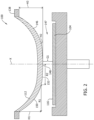
- Fig. 2 shows an enlarged view of portions of the CVD system 100 and Fig. 3 shows a bottom view of the upper window 112.
- Fig. 4 is an enlarged cross-section of a portion of the upper window 112 shown in Fig. 2 .
- Fig. 2 wherein portions of the CVD system 100 have been removed for illustration, the shape of the upper window 112 is shown in greater detail. It will be understood that the dimensions of the upper window 112 are not drawn to scale in Fig. 2 and, more particularly, that the curvatures of the upper window 112 are exaggerated for purposes of illustration.
- the lower face 146 defines a lowermost point, indicated generally at 148.
- the lowermost point 148 of the lower face 146 is the point wherein the gap 147 defined between the lower face 146 and the substrate surface 116 is at its most narrow.
- the lowermost point 148 is spaced a gap distance, indicated at G 1 , from the substrate 104.
- the lowermost point 148 of the lower face 146 is also be located at the radial center of the lower face 146, or, more generally, at the radial center of the upper window 112.
- the lower face 146 of the upper window 112 includes a radially outer surface 150 and a radially inner surface 152 circumscribed within the outer surface 150. More specifically, as shown in the embodiment of Fig. 2 , the outer surface 150 extends a first radial distance, indicated at R 1 , radially inward from the rim 138 to the inner surface 152. The outer surface 150 is curved such that the outer surface also extends a height, indicated generally at H 1 , from the rim 138 to the inner surface 152. More specifically, in the example embodiment, the outer surface 150 of the lower face 146 has a constant curvature between the rim 138 and the inner surface 152. Alternatively, the outer surface 150 may include multiple surfaces having varied curvatures from one another.
- the inner surface 152 of the lower face 146 extends a second radial distance in a plane tangential to the lowermost point 148 (also a "radial center" of the upper window in the example embodiment), indicated at R 2 , between the outer surface 150 and the lowermost point 148 of the upper window 112.
- the radius R 2 of the inner surface 152 may be between 5 millimeters and 200 millimeters, between 25 millimeters and 125 millimeters, between 50 millimeters and 100 millimeters, or between 70 millimeters and 90 millimeters. In the embodiment of Fig. 2 , the radius R 2 of the inner surface 152 is approximately 75 millimeters.
- the inner surface 152 may also be curved such that the inner surface 152 also extends a height, indicated at H 2 between the outer surface 150 and the lowermost point 148 (i.e., the radial center) of the upper window 112. As shown in the embodiment of Fig. 2 , the inner surface 152 has a constant curvature from the outer surface 150 to the lowermost point 148 and from the lowermost point 148 to a diametrically opposed portion of the outer surface 150. Alternatively, the inner surface 152 may include multiple surfaces having varied curvatures from one another.
- the lower face 146 extends an overall height, indicated at H 3 from the rim 138 to the lowermost point 148. More specifically, in the embodiment shown in Fig. 2 , the overall height H 3 is equal to the sum total of the height H 1 of the outer surface 150 and the height H 2 of the inner surface 152. The overall height H 3 may be between 6 millimeters and 20 millimeters, 8 millimeters and 16 millimeters, or 9 millimeters and 12 millimeters. In the embodiment of Fig. 2 , the overall height H 3 of the lower face 146 is approximately 10 millimeters.
- the radius of curvature of the outer surface 150 is suitably between 700 millimeters and 1,500 millimeters, between 800 and 1,400 millimeters, or between 900 millimeters and 1300 millimeters. In the embodiment shown in Fig. 2 , the radius of curvature of the outer surface 150 is 1,260 millimeters.
- the radius of curvature of the inner surface 152 is suitably between 3,000 millimeters and 13,000 millimeters, between 6,000 millimeters and 10,000 millimeters, or between 7,000 millimeters and 9,000 millimeters. In the embodiment shown in Fig. 2 , the radius of curvature of the inner surface 152 is 8,000 millimeters.
- Figs. 5-8 are graphs showing the measured thickness profiles of epitaxy deposited on the substrate surfaces for each of the test windows.
- the Y-axis in the graph represents the thickness in nanometers of epitaxy deposited on the substrate surface, with the zero adjusted to the lowest measured thickness on the substrate.
- the X-axis in the graph indicates the distance from the radial center of the substrate. More specifically, Fig. 5 shows the measured thickness profile 402 from the above tests, described with respect to Table 1, performed on the large curvature window.
- Fig. 6 shows the measured thickness profile 502 from the above tests performed on the large curvature window.
- Fig. 7 shows the measured thickness profile 602 from the above tests performed on the first dual curvature window, having an inner surface radius of 75 millimeters.
- Fig. 8 shows the measured thickness profile 702 from the above tests performed on the second dual curvature window, having an inner surface radius of 100 millimeters.
- the large curvature window resulted in significant dips 404 in the epitaxy thickness profile around one third of the radial distance from the center of the substrate (i.e., at +/- 50 millimeters from the center of the substrate).
- the dips 504 around the +/- 50 millimeter portion of the substrate were less pronounced with the small curvature window as compared with the large curvature window.
- the small curvature window resulted in high edge upticks 506 between the -150 millimeters to -125 millimeter range and between the 125 millimeter to 150 millimeter range on the substrate.
- the epitaxy deposited on the substrates using both the first dual curvature window and the second dual curvature window had reduced dips 604, 704 around the +/-50 millimeter radius range compared with the large curvature window.
- the epitaxy deposited on the substrate surfaces had reduced edge upticks 606, 706 between the -150 millimeters to -125 millimeter range and between the 125 millimeter to 150 millimeter range, as compared with the small curvature window.
- the dual curvature windows each resulted in an epitaxial deposition profile that had a lower relative thickness variation compared to the large and small curvature upper windows.
- test windows were used to measure the effects of operating the CVD system at different flow rates.
- the temperature of the processing chamber was maintained at 1100 degrees Celsius.
- the first dual curvature window resulted in an increased growth rate relative to the large curvature window.
- the first dual curvature window and the second dual curvature window were each tested in the CVD system and a trichlorosilane-hydrogen mixture was introduced into the CVD system at a flow rate of 7.6 standard-liters per minute. Average thickness of the epitaxy deposition and deposition time were measured to determine a growth rate in microns per minute. The results of the tests are provided in Table 3 below. Table 3: Growth Rate Comparison at Flow Rate of 7.6 slm Avg. Thickness (um) Depo. Time (sec) Growth Rate (um/min) Dual Curvature Window #1 2.431 102.5 1.428 Dual Curvature Window #2 2.519 102.5 1.481
- the second dual curvature window resulted in an increased growth rate relative to the first dual curvature window.
- the growth rate using the first dual curvature window at a flow rate of 7.6 standard-liters per minute was about the same as the growth rate as resulted from the large curvature window operating at an increased flow rate of 8.5 standard-liters per minute measured in the first test.
- process gas such as a trichlorosilane-hydrogen mixture
- a flow rate of at least about 5 standard-liters per minute, at least about 10 standard-liters per minute, or even at least about 15 standard-liters per minute may be introduced into the CVD system at a flow rate of at least about 5 standard-liters per minute, at least about 10 standard-liters per minute, or even at least about 15 standard-liters per minute, while maintaining a relative layer thickness variation of less than about 4% across the substrate surface, less than about 2% across the substrate surface, or even less than about 1% across the substrate surface.
- Carrier gas such as hydrogen
- Carrier gas may also be introduced at a higher flow rate, such as at least about 70 standard-liters per minute, at least about 80 standard-liters per minute, or even at least about 90 standard-liters per minute, while maintaining a relative layer thickness variation of less than about 4% across the substrate surface, less than about 2% across the substrate surface, or even less than about 1% across the substrate surface. Because the uniformity of the gas flow distribution across the substrate surface can be maintained at higher gas flow rates, the rate at which a given film or layer is deposited on a substrate may also be increased while maintaining uniformity in the layer thickness.
- standard-liter refers to one liter of the referenced gas at 0°C and 101.3 kPa (1013 millibar).
- the examples described are suitable for processing semiconductor wafers, such as silicon wafers, though may be used in other applications. Some of the examples are particularly suited for use in atmospheric-pressure silicon on silicon chemical vapor deposition epitaxy using gas mixtures including hydrogen, trichlorosilane, and diborane. Silicon precursors other than trichlorosilane may also be used, including dichlorosilane, silane, trisilane, tetrachlorosilane, methylsilane, pentasilane, neopentasilane, and other higher order silane precursors. Precursors other than silicon precursors may also be used, including germane, digermane, and other germanium precursors.
- Dopant gas species other than diborane may be used, including phosphine and arsine.
- the examples described may also be used in processes other than atmospheric-pressure silicon on silicon epitaxy, including reduced-pressure epitaxy (e.g., at pressures between about 10 Torr and about 750 Torr), silicon-germanium epitaxy, carbon-doped silicon epitaxy, and non-epitaxial chemical vapor deposition.
- the examples may also be used to process wafers other than silicon wafers, including wafers having germanium, gallium arsenide, indium phosphide, and silicon carbide.
- processing chambers including the upper windows of the present invention provide an improvement over known processing chambers.
- the upper windows of the present invention include two surfaces having different curvatures to direct the process flow during operation and facilitate providing a laminar flow of process gas across the substrate. As a result, uniformity in gas flow distribution across the substrate surface can be improved.
- CVD systems including the upper windows of the present invention provide the following advantages over the some conventional CVD systems: 1) reduced epitaxial dips on the substrate; 2) reduced epitaxial upticks on the substrate near the outer perimeter of the substrate; 3) reduced processing time for epitaxial deposition on substrates; and 4) improved lifespan of semiconductor wafers.
Landscapes
- Chemical & Material Sciences (AREA)
- Metallurgy (AREA)
- Chemical Kinetics & Catalysis (AREA)
- Engineering & Computer Science (AREA)
- Materials Engineering (AREA)
- General Chemical & Material Sciences (AREA)
- Organic Chemistry (AREA)
- Mechanical Engineering (AREA)
- Health & Medical Sciences (AREA)
- Toxicology (AREA)
- Physics & Mathematics (AREA)
- Fluid Mechanics (AREA)
- Crystallography & Structural Chemistry (AREA)
- Chemical Vapour Deposition (AREA)
Claims (10)
- Un système (100) de dépôt d'une couche sur un substrat (104), le système comprenant :une chambre de traitement (102) définissant une entrée de gaz (103) pour introduire du gaz (110) dans la chambre de traitement et une sortie de gaz (105) pour permettre au gaz de sortir de la chambre de traitement ;un support de substrat positionné à l'intérieur de la chambre de traitement et configuré pour recevoir un substrat ; etune fenêtre supérieure (112) comprenant :un cadre (138) pour fixer la fenêtre à la chambre de traitement ; etun corps transparent (142) relié au cadre, le corps s'étendant entre une première face convexe et une seconde face opposée, la première face comprenant une surface radialement extérieure (150) et une surface radialement intérieure (152) circonscrite dans la surface extérieure, la surface extérieure s'étendant radialement depuis le cadre jusqu'à la surface intérieure et la surface intérieure s'étendant radialement vers l'intérieur depuis la surface extérieure jusqu'à un centre radial de la fenêtre, caractérisé en ce quela surface extérieure a un premier rayon de courbure et la surface intérieure présentant un second rayon de courbure différent du premier rayon de courbure,la première face convexe est espacée du support de substrat pour définir un espace d'air (147) entre les deux, et la fenêtre supérieure est positionnée à l'intérieur de la chambre de traitement pour diriger le gaz depuis l'entrée de gaz (103), à travers l'espace d'air, et jusqu'à la sortie de gaz (105).
- Le système de la revendication 1, dans lequel la surface intérieure est positionnée de manière à être alignée verticalement avec le substrat lorsque le substrat est reçu sur le support de substrat et dans lequel le second rayon de courbure est supérieur au premier rayon de courbure.
- Le système de la revendication 2, dans lequel le rapport entre le second rayon de courbure et le premier rayon de courbure est compris entre 100:1 et 1.1:1, de préférence dans lequel le rapport est compris entre 10:1 et 5:1.
- Le système de la revendication 1, dans lequel la surface intérieure et la surface extérieure sont chacune positionnées pour être alignées verticalement avec au moins une partie du substrat lorsque le substrat est reçu sur le support de substrat.
- Le système de la revendication 1, dans lequel l'espace d'air diminue entre la surface extérieure et la surface intérieure.
- Le système de la revendication 1, dans lequel la surface intérieure définit un rayon s'étendant dans un plan tangentiel à un centre radial de la fenêtre supérieure, le rayon s'étendant du centre radial à la surface extérieure, et dans lequel le rayon de la surface intérieure est compris entre 5 millimètres et 200 millimètres.
- Le système de la revendication 1, dans lequel la seconde face présente une courbure concave.
- Le système de la revendication 1, dans lequel le cadre (138) est un rebord entourant la première face et configuré pour être couplé à la chambre de traitement, dans lequel la surface extérieure s'étend sur une première hauteur entre le rebord et la surface intérieure, dans lequel la surface intérieure s'étend sur une deuxième hauteur entre la surface extérieure et un centre radial de la fenêtre supérieure, dans lequel la première hauteur est supérieure à la seconde hauteur.
- Une méthode de dépôt d'une couche sur un substrat, la méthode comprenant :fournir un substrat sur le support de substrat à l'intérieur de la chambre de traitement du système selon l'une quelconque des revendications 1 à 8 ; etdiriger un flux de gaz à travers l'entrée de gaz, dans l'espace d'air entre la première face et le substrat, et vers la sortie de gaz.
- La méthode de la revendication 9, dans laquelle le flux de gaz est fourni à un débit supérieur à 2 litres standard par minute et dans laquelle une variation relative de l'épaisseur de la couche déposée sur le substrat est inférieure à environ 2 %.
Applications Claiming Priority (2)
| Application Number | Priority Date | Filing Date | Title |
|---|---|---|---|
| US202062706452P | 2020-08-18 | 2020-08-18 | |
| PCT/US2021/045873 WO2022040031A1 (fr) | 2020-08-18 | 2021-08-13 | Fenêtre pour systèmes de dépôt chimique en phase vapeur et procédés associés |
Publications (2)
| Publication Number | Publication Date |
|---|---|
| EP4200462A1 EP4200462A1 (fr) | 2023-06-28 |
| EP4200462B1 true EP4200462B1 (fr) | 2025-05-21 |
Family
ID=77655665
Family Applications (1)
| Application Number | Title | Priority Date | Filing Date |
|---|---|---|---|
| EP21766306.1A Active EP4200462B1 (fr) | 2020-08-18 | 2021-08-13 | Fenêtre pour systèmes de dépôt chimique en phase vapeur et procédés associés |
Country Status (7)
| Country | Link |
|---|---|
| US (2) | US12084770B2 (fr) |
| EP (1) | EP4200462B1 (fr) |
| JP (1) | JP7607748B2 (fr) |
| KR (1) | KR102859279B1 (fr) |
| CN (1) | CN116096941B (fr) |
| TW (2) | TWI896428B (fr) |
| WO (1) | WO2022040031A1 (fr) |
Families Citing this family (2)
| Publication number | Priority date | Publication date | Assignee | Title |
|---|---|---|---|---|
| US12221696B2 (en) * | 2022-05-27 | 2025-02-11 | Applied Materials, Inc. | Process kits and related methods for processing chambers to facilitate deposition process adjustability |
| US12456614B2 (en) | 2022-05-27 | 2025-10-28 | Applied Materials, Inc. | Process kits and related methods for processing chambers to facilitate deposition process adjustability |
Citations (2)
| Publication number | Priority date | Publication date | Assignee | Title |
|---|---|---|---|---|
| US5506403A (en) * | 1993-10-29 | 1996-04-09 | Kabushiki Kaisha Toshiba | Radiation image intensifier having a metal convex-14 Spherical radiation window which is thicker around the periphery than at the center |
| US20140199056A1 (en) * | 2013-01-16 | 2014-07-17 | Applied Materials, Inc. | Quartz upper and lower domes |
Family Cites Families (13)
| Publication number | Priority date | Publication date | Assignee | Title |
|---|---|---|---|---|
| US6099648A (en) * | 1997-08-06 | 2000-08-08 | Applied Materials, Inc. | Domed wafer reactor vessel window with reduced stress at atmospheric and above atmospheric pressures |
| US6143079A (en) | 1998-11-19 | 2000-11-07 | Asm America, Inc. | Compact process chamber for improved process uniformity |
| JP2007504215A (ja) | 2003-09-03 | 2007-03-01 | バイオフォームズ | 生体分子を急速に結晶化するための方法及び装置 |
| JP5029340B2 (ja) * | 2007-12-14 | 2012-09-19 | 信越半導体株式会社 | エピタキシャル成長方法 |
| DE102008034260B4 (de) | 2008-07-16 | 2014-06-26 | Siltronic Ag | Verfahren zum Abscheiden einer Schicht auf einer Halbleiterscheibe mittels CVD in einer Kammer und Kammer zum Abscheiden einer Schicht auf einer Halbleiterscheibe mittels CVD |
| US10344380B2 (en) * | 2013-02-11 | 2019-07-09 | Globalwafers Co., Ltd. | Liner assemblies for substrate processing systems |
| KR20140102880A (ko) | 2013-02-15 | 2014-08-25 | 삼성전자주식회사 | 반도체 발광소자 제조방법 및 화학 기상 증착 장치 |
| WO2014143499A1 (fr) | 2013-03-15 | 2014-09-18 | Applied Materials, Inc. | Arbre support de suscepteur muni de lentilles d'accord d'uniformité pour processus epi |
| JP6052070B2 (ja) | 2013-06-17 | 2016-12-27 | 株式会社Sumco | エピタキシャルウェーハの製造方法及びその製造装置 |
| TWI734668B (zh) * | 2014-06-23 | 2021-08-01 | 美商應用材料股份有限公司 | 在epi腔室中的基材熱控制 |
| US20160071749A1 (en) | 2014-09-05 | 2016-03-10 | Applied Materials, Inc. | Upper dome for epi chamber |
| KR20170048578A (ko) * | 2014-09-05 | 2017-05-08 | 어플라이드 머티어리얼스, 인코포레이티드 | 분위기 에피택셜 퇴적 챔버 |
| WO2019046453A1 (fr) * | 2017-08-30 | 2019-03-07 | Applied Materials, Inc. | Élimination de contaminants à haute température de système d'épitaxie intégré |
-
2021
- 2021-08-12 US US17/400,722 patent/US12084770B2/en active Active
- 2021-08-13 EP EP21766306.1A patent/EP4200462B1/fr active Active
- 2021-08-13 JP JP2023512164A patent/JP7607748B2/ja active Active
- 2021-08-13 WO PCT/US2021/045873 patent/WO2022040031A1/fr not_active Ceased
- 2021-08-13 KR KR1020237009035A patent/KR102859279B1/ko active Active
- 2021-08-13 CN CN202180062841.3A patent/CN116096941B/zh active Active
- 2021-08-17 TW TW113144330A patent/TWI896428B/zh active
- 2021-08-17 TW TW110130361A patent/TWI867238B/zh active
-
2024
- 2024-08-12 US US18/800,465 patent/US20240401201A1/en active Pending
Patent Citations (2)
| Publication number | Priority date | Publication date | Assignee | Title |
|---|---|---|---|---|
| US5506403A (en) * | 1993-10-29 | 1996-04-09 | Kabushiki Kaisha Toshiba | Radiation image intensifier having a metal convex-14 Spherical radiation window which is thicker around the periphery than at the center |
| US20140199056A1 (en) * | 2013-01-16 | 2014-07-17 | Applied Materials, Inc. | Quartz upper and lower domes |
Also Published As
| Publication number | Publication date |
|---|---|
| US20240401201A1 (en) | 2024-12-05 |
| TWI896428B (zh) | 2025-09-01 |
| CN116096941A (zh) | 2023-05-09 |
| JP2023539137A (ja) | 2023-09-13 |
| US20220056583A1 (en) | 2022-02-24 |
| KR102859279B1 (ko) | 2025-09-17 |
| TWI867238B (zh) | 2024-12-21 |
| CN116096941B (zh) | 2025-04-25 |
| TW202225468A (zh) | 2022-07-01 |
| US12084770B2 (en) | 2024-09-10 |
| TW202509276A (zh) | 2025-03-01 |
| KR20230053648A (ko) | 2023-04-21 |
| WO2022040031A1 (fr) | 2022-02-24 |
| JP7607748B2 (ja) | 2024-12-27 |
| EP4200462A1 (fr) | 2023-06-28 |
Similar Documents
| Publication | Publication Date | Title |
|---|---|---|
| US20240401201A1 (en) | Window for chemical vapor deposition systems and related methods | |
| US5252133A (en) | Vertically oriented CVD apparatus including gas inlet tube having gas injection holes | |
| US8999063B2 (en) | Susceptor, semiconductor manufacturing apparatus, and semiconductor manufacturing method | |
| US20100029066A1 (en) | Susceptor, vapor phase growth apparatus, and method of manufacturing epitaxial wafer | |
| US20200354853A1 (en) | Epitaxial growth apparatus, preheat ring, and method of manufacturing epitaxial wafer using these | |
| JPH0831758A (ja) | 気相成長方法およびその装置 | |
| US12503792B2 (en) | Methods for manufacturing a semiconductor wafer using a preheat ring in a wafer reactor | |
| US20210180208A1 (en) | Vapor phase growth apparatus | |
| US10184193B2 (en) | Epitaxy reactor and susceptor system for improved epitaxial wafer flatness | |
| US11926892B2 (en) | Methods for conditioning a processing reactor | |
| US20210381128A1 (en) | Vapor phase growth apparatus | |
| KR20230125028A (ko) | 반도체 웨이퍼 반응기에서의 복사열 캡을 위한 시스템및 방법들 | |
| WO2021225047A1 (fr) | Dispositif de dépôt et plaque | |
| US11515196B1 (en) | Methods for etching a semiconductor structure and for conditioning a processing reactor | |
| JPH06302519A (ja) | 半導体製造装置 | |
| US20260015766A1 (en) | Reaction apparatus and methods for depositing an epitaxial layer on a semiconductor structure with side injection | |
| US20230047866A1 (en) | Methods for etching a semiconductor structure and for conditioning a processing reactor | |
| US20260071352A1 (en) | SiC EPITAXIAL WAFER | |
| TW202427669A (zh) | 用於磊晶處理之承載盤及包括該承載盤之磊晶反應器 | |
| JPS5877224A (ja) | 気相成長方法 |
Legal Events
| Date | Code | Title | Description |
|---|---|---|---|
| STAA | Information on the status of an ep patent application or granted ep patent |
Free format text: STATUS: UNKNOWN |
|
| STAA | Information on the status of an ep patent application or granted ep patent |
Free format text: STATUS: THE INTERNATIONAL PUBLICATION HAS BEEN MADE |
|
| PUAI | Public reference made under article 153(3) epc to a published international application that has entered the european phase |
Free format text: ORIGINAL CODE: 0009012 |
|
| STAA | Information on the status of an ep patent application or granted ep patent |
Free format text: STATUS: REQUEST FOR EXAMINATION WAS MADE |
|
| 17P | Request for examination filed |
Effective date: 20230315 |
|
| AK | Designated contracting states |
Kind code of ref document: A1 Designated state(s): AL AT BE BG CH CY CZ DE DK EE ES FI FR GB GR HR HU IE IS IT LI LT LU LV MC MK MT NL NO PL PT RO RS SE SI SK SM TR |
|
| DAV | Request for validation of the european patent (deleted) | ||
| DAX | Request for extension of the european patent (deleted) | ||
| STAA | Information on the status of an ep patent application or granted ep patent |
Free format text: STATUS: EXAMINATION IS IN PROGRESS |
|
| 17Q | First examination report despatched |
Effective date: 20240123 |
|
| GRAP | Despatch of communication of intention to grant a patent |
Free format text: ORIGINAL CODE: EPIDOSNIGR1 |
|
| STAA | Information on the status of an ep patent application or granted ep patent |
Free format text: STATUS: GRANT OF PATENT IS INTENDED |
|
| RIC1 | Information provided on ipc code assigned before grant |
Ipc: C30B 25/16 20060101ALI20241206BHEP Ipc: C23C 16/48 20060101ALI20241206BHEP Ipc: C23C 16/455 20060101AFI20241206BHEP |
|
| INTG | Intention to grant announced |
Effective date: 20241219 |
|
| GRAS | Grant fee paid |
Free format text: ORIGINAL CODE: EPIDOSNIGR3 |
|
| GRAA | (expected) grant |
Free format text: ORIGINAL CODE: 0009210 |
|
| STAA | Information on the status of an ep patent application or granted ep patent |
Free format text: STATUS: THE PATENT HAS BEEN GRANTED |
|
| AK | Designated contracting states |
Kind code of ref document: B1 Designated state(s): AL AT BE BG CH CY CZ DE DK EE ES FI FR GB GR HR HU IE IS IT LI LT LU LV MC MK MT NL NO PL PT RO RS SE SI SK SM TR |
|
| REG | Reference to a national code |
Ref country code: GB Ref legal event code: FG4D |
|
| REG | Reference to a national code |
Ref country code: CH Ref legal event code: EP |
|
| REG | Reference to a national code |
Ref country code: DE Ref legal event code: R096 Ref document number: 602021031172 Country of ref document: DE |
|
| REG | Reference to a national code |
Ref country code: IE Ref legal event code: FG4D |
|
| REG | Reference to a national code |
Ref country code: NL Ref legal event code: MP Effective date: 20250521 |
|
| PG25 | Lapsed in a contracting state [announced via postgrant information from national office to epo] |
Ref country code: PT Free format text: LAPSE BECAUSE OF FAILURE TO SUBMIT A TRANSLATION OF THE DESCRIPTION OR TO PAY THE FEE WITHIN THE PRESCRIBED TIME-LIMIT Effective date: 20250922 Ref country code: FI Free format text: LAPSE BECAUSE OF FAILURE TO SUBMIT A TRANSLATION OF THE DESCRIPTION OR TO PAY THE FEE WITHIN THE PRESCRIBED TIME-LIMIT Effective date: 20250521 Ref country code: ES Free format text: LAPSE BECAUSE OF FAILURE TO SUBMIT A TRANSLATION OF THE DESCRIPTION OR TO PAY THE FEE WITHIN THE PRESCRIBED TIME-LIMIT Effective date: 20250521 |
|
| PGFP | Annual fee paid to national office [announced via postgrant information from national office to epo] |
Ref country code: DE Payment date: 20250827 Year of fee payment: 5 |
|
| REG | Reference to a national code |
Ref country code: LT Ref legal event code: MG9D |
|
| PG25 | Lapsed in a contracting state [announced via postgrant information from national office to epo] |
Ref country code: NO Free format text: LAPSE BECAUSE OF FAILURE TO SUBMIT A TRANSLATION OF THE DESCRIPTION OR TO PAY THE FEE WITHIN THE PRESCRIBED TIME-LIMIT Effective date: 20250821 Ref country code: GR Free format text: LAPSE BECAUSE OF FAILURE TO SUBMIT A TRANSLATION OF THE DESCRIPTION OR TO PAY THE FEE WITHIN THE PRESCRIBED TIME-LIMIT Effective date: 20250822 |
|
| PG25 | Lapsed in a contracting state [announced via postgrant information from national office to epo] |
Ref country code: NL Free format text: LAPSE BECAUSE OF FAILURE TO SUBMIT A TRANSLATION OF THE DESCRIPTION OR TO PAY THE FEE WITHIN THE PRESCRIBED TIME-LIMIT Effective date: 20250521 Ref country code: PL Free format text: LAPSE BECAUSE OF FAILURE TO SUBMIT A TRANSLATION OF THE DESCRIPTION OR TO PAY THE FEE WITHIN THE PRESCRIBED TIME-LIMIT Effective date: 20250521 |
|
| PG25 | Lapsed in a contracting state [announced via postgrant information from national office to epo] |
Ref country code: BG Free format text: LAPSE BECAUSE OF FAILURE TO SUBMIT A TRANSLATION OF THE DESCRIPTION OR TO PAY THE FEE WITHIN THE PRESCRIBED TIME-LIMIT Effective date: 20250521 |
|
| PG25 | Lapsed in a contracting state [announced via postgrant information from national office to epo] |
Ref country code: HR Free format text: LAPSE BECAUSE OF FAILURE TO SUBMIT A TRANSLATION OF THE DESCRIPTION OR TO PAY THE FEE WITHIN THE PRESCRIBED TIME-LIMIT Effective date: 20250521 |
|
| PGFP | Annual fee paid to national office [announced via postgrant information from national office to epo] |
Ref country code: FR Payment date: 20250825 Year of fee payment: 5 |
|
| PG25 | Lapsed in a contracting state [announced via postgrant information from national office to epo] |
Ref country code: RS Free format text: LAPSE BECAUSE OF FAILURE TO SUBMIT A TRANSLATION OF THE DESCRIPTION OR TO PAY THE FEE WITHIN THE PRESCRIBED TIME-LIMIT Effective date: 20250821 |
|
| PG25 | Lapsed in a contracting state [announced via postgrant information from national office to epo] |
Ref country code: IS Free format text: LAPSE BECAUSE OF FAILURE TO SUBMIT A TRANSLATION OF THE DESCRIPTION OR TO PAY THE FEE WITHIN THE PRESCRIBED TIME-LIMIT Effective date: 20250921 |
|
| PG25 | Lapsed in a contracting state [announced via postgrant information from national office to epo] |
Ref country code: LV Free format text: LAPSE BECAUSE OF FAILURE TO SUBMIT A TRANSLATION OF THE DESCRIPTION OR TO PAY THE FEE WITHIN THE PRESCRIBED TIME-LIMIT Effective date: 20250521 |
|
| REG | Reference to a national code |
Ref country code: AT Ref legal event code: MK05 Ref document number: 1796812 Country of ref document: AT Kind code of ref document: T Effective date: 20250521 |
|
| PG25 | Lapsed in a contracting state [announced via postgrant information from national office to epo] |
Ref country code: AT Free format text: LAPSE BECAUSE OF FAILURE TO SUBMIT A TRANSLATION OF THE DESCRIPTION OR TO PAY THE FEE WITHIN THE PRESCRIBED TIME-LIMIT Effective date: 20250521 Ref country code: SM Free format text: LAPSE BECAUSE OF FAILURE TO SUBMIT A TRANSLATION OF THE DESCRIPTION OR TO PAY THE FEE WITHIN THE PRESCRIBED TIME-LIMIT Effective date: 20250521 Ref country code: DK Free format text: LAPSE BECAUSE OF FAILURE TO SUBMIT A TRANSLATION OF THE DESCRIPTION OR TO PAY THE FEE WITHIN THE PRESCRIBED TIME-LIMIT Effective date: 20250521 |
|
| PG25 | Lapsed in a contracting state [announced via postgrant information from national office to epo] |
Ref country code: CZ Free format text: LAPSE BECAUSE OF FAILURE TO SUBMIT A TRANSLATION OF THE DESCRIPTION OR TO PAY THE FEE WITHIN THE PRESCRIBED TIME-LIMIT Effective date: 20250521 |
|
| PG25 | Lapsed in a contracting state [announced via postgrant information from national office to epo] |
Ref country code: EE Free format text: LAPSE BECAUSE OF FAILURE TO SUBMIT A TRANSLATION OF THE DESCRIPTION OR TO PAY THE FEE WITHIN THE PRESCRIBED TIME-LIMIT Effective date: 20250521 |
|
| PG25 | Lapsed in a contracting state [announced via postgrant information from national office to epo] |
Ref country code: SK Free format text: LAPSE BECAUSE OF FAILURE TO SUBMIT A TRANSLATION OF THE DESCRIPTION OR TO PAY THE FEE WITHIN THE PRESCRIBED TIME-LIMIT Effective date: 20250521 |
|
| PG25 | Lapsed in a contracting state [announced via postgrant information from national office to epo] |
Ref country code: IT Free format text: LAPSE BECAUSE OF FAILURE TO SUBMIT A TRANSLATION OF THE DESCRIPTION OR TO PAY THE FEE WITHIN THE PRESCRIBED TIME-LIMIT Effective date: 20250521 |
|
| REG | Reference to a national code |
Ref country code: DE Ref legal event code: R097 Ref document number: 602021031172 Country of ref document: DE |
|
| PG25 | Lapsed in a contracting state [announced via postgrant information from national office to epo] |
Ref country code: RO Free format text: LAPSE BECAUSE OF FAILURE TO SUBMIT A TRANSLATION OF THE DESCRIPTION OR TO PAY THE FEE WITHIN THE PRESCRIBED TIME-LIMIT Effective date: 20250521 |
|
| REG | Reference to a national code |
Ref country code: CH Ref legal event code: H13 Free format text: ST27 STATUS EVENT CODE: U-0-0-H10-H13 (AS PROVIDED BY THE NATIONAL OFFICE) Effective date: 20260324 |
|
| PLBE | No opposition filed within time limit |
Free format text: ORIGINAL CODE: 0009261 |
|
| STAA | Information on the status of an ep patent application or granted ep patent |
Free format text: STATUS: NO OPPOSITION FILED WITHIN TIME LIMIT |
|
| PG25 | Lapsed in a contracting state [announced via postgrant information from national office to epo] |
Ref country code: MC Free format text: LAPSE BECAUSE OF FAILURE TO SUBMIT A TRANSLATION OF THE DESCRIPTION OR TO PAY THE FEE WITHIN THE PRESCRIBED TIME-LIMIT Effective date: 20250521 |
|
| REG | Reference to a national code |
Ref country code: CH Ref legal event code: L10 Free format text: ST27 STATUS EVENT CODE: U-0-0-L10-L00 (AS PROVIDED BY THE NATIONAL OFFICE) Effective date: 20260402 |
|
| PG25 | Lapsed in a contracting state [announced via postgrant information from national office to epo] |
Ref country code: LU Free format text: LAPSE BECAUSE OF NON-PAYMENT OF DUE FEES Effective date: 20250813 |
|
| PG25 | Lapsed in a contracting state [announced via postgrant information from national office to epo] |
Ref country code: CH Free format text: LAPSE BECAUSE OF NON-PAYMENT OF DUE FEES Effective date: 20250831 |
|
| 26N | No opposition filed |
Effective date: 20260224 |