EP4205178B1 - Panneau d'affichage - Google Patents
Panneau d'affichage Download PDFInfo
- Publication number
- EP4205178B1 EP4205178B1 EP21946474.0A EP21946474A EP4205178B1 EP 4205178 B1 EP4205178 B1 EP 4205178B1 EP 21946474 A EP21946474 A EP 21946474A EP 4205178 B1 EP4205178 B1 EP 4205178B1
- Authority
- EP
- European Patent Office
- Prior art keywords
- signal lines
- layer
- voltage signal
- display panel
- signal line
- Prior art date
- Legal status (The legal status is an assumption and is not a legal conclusion. Google has not performed a legal analysis and makes no representation as to the accuracy of the status listed.)
- Active
Links
Images


















Classifications
-
- G—PHYSICS
- G09—EDUCATION; CRYPTOGRAPHY; DISPLAY; ADVERTISING; SEALS
- G09G—ARRANGEMENTS OR CIRCUITS FOR CONTROL OF INDICATING DEVICES USING STATIC MEANS TO PRESENT VARIABLE INFORMATION
- G09G3/00—Control arrangements or circuits, of interest only in connection with visual indicators other than cathode-ray tubes
- G09G3/20—Control arrangements or circuits, of interest only in connection with visual indicators other than cathode-ray tubes for presentation of an assembly of a number of characters, e.g. a page, by composing the assembly by combination of individual elements arranged in a matrix no fixed position being assigned to or needed to be assigned to the individual characters or partial characters
- G09G3/22—Control arrangements or circuits, of interest only in connection with visual indicators other than cathode-ray tubes for presentation of an assembly of a number of characters, e.g. a page, by composing the assembly by combination of individual elements arranged in a matrix no fixed position being assigned to or needed to be assigned to the individual characters or partial characters using controlled light sources
- G09G3/30—Control arrangements or circuits, of interest only in connection with visual indicators other than cathode-ray tubes for presentation of an assembly of a number of characters, e.g. a page, by composing the assembly by combination of individual elements arranged in a matrix no fixed position being assigned to or needed to be assigned to the individual characters or partial characters using controlled light sources using electroluminescent panels
- G09G3/32—Control arrangements or circuits, of interest only in connection with visual indicators other than cathode-ray tubes for presentation of an assembly of a number of characters, e.g. a page, by composing the assembly by combination of individual elements arranged in a matrix no fixed position being assigned to or needed to be assigned to the individual characters or partial characters using controlled light sources using electroluminescent panels semiconductive, e.g. using light-emitting diodes [LED]
- G09G3/3208—Control arrangements or circuits, of interest only in connection with visual indicators other than cathode-ray tubes for presentation of an assembly of a number of characters, e.g. a page, by composing the assembly by combination of individual elements arranged in a matrix no fixed position being assigned to or needed to be assigned to the individual characters or partial characters using controlled light sources using electroluminescent panels semiconductive, e.g. using light-emitting diodes [LED] organic, e.g. using organic light-emitting diodes [OLED]
-
- H—ELECTRICITY
- H10—SEMICONDUCTOR DEVICES; ELECTRIC SOLID-STATE DEVICES NOT OTHERWISE PROVIDED FOR
- H10K—ORGANIC ELECTRIC SOLID-STATE DEVICES
- H10K59/00—Integrated devices, or assemblies of multiple devices, comprising at least one organic light-emitting element covered by group H10K50/00
- H10K59/10—OLED displays
- H10K59/12—Active-matrix OLED [AMOLED] displays
- H10K59/131—Interconnections, e.g. wiring lines or terminals
-
- G—PHYSICS
- G09—EDUCATION; CRYPTOGRAPHY; DISPLAY; ADVERTISING; SEALS
- G09G—ARRANGEMENTS OR CIRCUITS FOR CONTROL OF INDICATING DEVICES USING STATIC MEANS TO PRESENT VARIABLE INFORMATION
- G09G3/00—Control arrangements or circuits, of interest only in connection with visual indicators other than cathode-ray tubes
- G09G3/20—Control arrangements or circuits, of interest only in connection with visual indicators other than cathode-ray tubes for presentation of an assembly of a number of characters, e.g. a page, by composing the assembly by combination of individual elements arranged in a matrix no fixed position being assigned to or needed to be assigned to the individual characters or partial characters
- G09G3/22—Control arrangements or circuits, of interest only in connection with visual indicators other than cathode-ray tubes for presentation of an assembly of a number of characters, e.g. a page, by composing the assembly by combination of individual elements arranged in a matrix no fixed position being assigned to or needed to be assigned to the individual characters or partial characters using controlled light sources
- G09G3/30—Control arrangements or circuits, of interest only in connection with visual indicators other than cathode-ray tubes for presentation of an assembly of a number of characters, e.g. a page, by composing the assembly by combination of individual elements arranged in a matrix no fixed position being assigned to or needed to be assigned to the individual characters or partial characters using controlled light sources using electroluminescent panels
- G09G3/32—Control arrangements or circuits, of interest only in connection with visual indicators other than cathode-ray tubes for presentation of an assembly of a number of characters, e.g. a page, by composing the assembly by combination of individual elements arranged in a matrix no fixed position being assigned to or needed to be assigned to the individual characters or partial characters using controlled light sources using electroluminescent panels semiconductive, e.g. using light-emitting diodes [LED]
- G09G3/3208—Control arrangements or circuits, of interest only in connection with visual indicators other than cathode-ray tubes for presentation of an assembly of a number of characters, e.g. a page, by composing the assembly by combination of individual elements arranged in a matrix no fixed position being assigned to or needed to be assigned to the individual characters or partial characters using controlled light sources using electroluminescent panels semiconductive, e.g. using light-emitting diodes [LED] organic, e.g. using organic light-emitting diodes [OLED]
- G09G3/3225—Control arrangements or circuits, of interest only in connection with visual indicators other than cathode-ray tubes for presentation of an assembly of a number of characters, e.g. a page, by composing the assembly by combination of individual elements arranged in a matrix no fixed position being assigned to or needed to be assigned to the individual characters or partial characters using controlled light sources using electroluminescent panels semiconductive, e.g. using light-emitting diodes [LED] organic, e.g. using organic light-emitting diodes [OLED] using an active matrix
- G09G3/3233—Control arrangements or circuits, of interest only in connection with visual indicators other than cathode-ray tubes for presentation of an assembly of a number of characters, e.g. a page, by composing the assembly by combination of individual elements arranged in a matrix no fixed position being assigned to or needed to be assigned to the individual characters or partial characters using controlled light sources using electroluminescent panels semiconductive, e.g. using light-emitting diodes [LED] organic, e.g. using organic light-emitting diodes [OLED] using an active matrix with pixel circuitry controlling the current through the light-emitting element
-
- G—PHYSICS
- G09—EDUCATION; CRYPTOGRAPHY; DISPLAY; ADVERTISING; SEALS
- G09G—ARRANGEMENTS OR CIRCUITS FOR CONTROL OF INDICATING DEVICES USING STATIC MEANS TO PRESENT VARIABLE INFORMATION
- G09G3/00—Control arrangements or circuits, of interest only in connection with visual indicators other than cathode-ray tubes
- G09G3/20—Control arrangements or circuits, of interest only in connection with visual indicators other than cathode-ray tubes for presentation of an assembly of a number of characters, e.g. a page, by composing the assembly by combination of individual elements arranged in a matrix no fixed position being assigned to or needed to be assigned to the individual characters or partial characters
- G09G3/22—Control arrangements or circuits, of interest only in connection with visual indicators other than cathode-ray tubes for presentation of an assembly of a number of characters, e.g. a page, by composing the assembly by combination of individual elements arranged in a matrix no fixed position being assigned to or needed to be assigned to the individual characters or partial characters using controlled light sources
- G09G3/30—Control arrangements or circuits, of interest only in connection with visual indicators other than cathode-ray tubes for presentation of an assembly of a number of characters, e.g. a page, by composing the assembly by combination of individual elements arranged in a matrix no fixed position being assigned to or needed to be assigned to the individual characters or partial characters using controlled light sources using electroluminescent panels
- G09G3/32—Control arrangements or circuits, of interest only in connection with visual indicators other than cathode-ray tubes for presentation of an assembly of a number of characters, e.g. a page, by composing the assembly by combination of individual elements arranged in a matrix no fixed position being assigned to or needed to be assigned to the individual characters or partial characters using controlled light sources using electroluminescent panels semiconductive, e.g. using light-emitting diodes [LED]
- G09G3/3208—Control arrangements or circuits, of interest only in connection with visual indicators other than cathode-ray tubes for presentation of an assembly of a number of characters, e.g. a page, by composing the assembly by combination of individual elements arranged in a matrix no fixed position being assigned to or needed to be assigned to the individual characters or partial characters using controlled light sources using electroluminescent panels semiconductive, e.g. using light-emitting diodes [LED] organic, e.g. using organic light-emitting diodes [OLED]
- G09G3/3275—Details of drivers for data electrodes
- G09G3/3291—Details of drivers for data electrodes in which the data driver supplies a variable data voltage for setting the current through, or the voltage across, the light-emitting elements
-
- H—ELECTRICITY
- H10—SEMICONDUCTOR DEVICES; ELECTRIC SOLID-STATE DEVICES NOT OTHERWISE PROVIDED FOR
- H10D—INORGANIC ELECTRIC SEMICONDUCTOR DEVICES
- H10D86/00—Integrated devices formed in or on insulating or conducting substrates, e.g. formed in silicon-on-insulator [SOI] substrates or on stainless steel or glass substrates
- H10D86/40—Integrated devices formed in or on insulating or conducting substrates, e.g. formed in silicon-on-insulator [SOI] substrates or on stainless steel or glass substrates characterised by multiple TFTs
- H10D86/441—Interconnections, e.g. scanning lines
-
- H—ELECTRICITY
- H10—SEMICONDUCTOR DEVICES; ELECTRIC SOLID-STATE DEVICES NOT OTHERWISE PROVIDED FOR
- H10D—INORGANIC ELECTRIC SEMICONDUCTOR DEVICES
- H10D86/00—Integrated devices formed in or on insulating or conducting substrates, e.g. formed in silicon-on-insulator [SOI] substrates or on stainless steel or glass substrates
- H10D86/40—Integrated devices formed in or on insulating or conducting substrates, e.g. formed in silicon-on-insulator [SOI] substrates or on stainless steel or glass substrates characterised by multiple TFTs
- H10D86/60—Integrated devices formed in or on insulating or conducting substrates, e.g. formed in silicon-on-insulator [SOI] substrates or on stainless steel or glass substrates characterised by multiple TFTs wherein the TFTs are in active matrices
-
- H—ELECTRICITY
- H10—SEMICONDUCTOR DEVICES; ELECTRIC SOLID-STATE DEVICES NOT OTHERWISE PROVIDED FOR
- H10K—ORGANIC ELECTRIC SOLID-STATE DEVICES
- H10K59/00—Integrated devices, or assemblies of multiple devices, comprising at least one organic light-emitting element covered by group H10K50/00
- H10K59/10—OLED displays
- H10K59/12—Active-matrix OLED [AMOLED] displays
- H10K59/124—Insulating layers formed between TFT elements and OLED elements
-
- G—PHYSICS
- G09—EDUCATION; CRYPTOGRAPHY; DISPLAY; ADVERTISING; SEALS
- G09G—ARRANGEMENTS OR CIRCUITS FOR CONTROL OF INDICATING DEVICES USING STATIC MEANS TO PRESENT VARIABLE INFORMATION
- G09G2300/00—Aspects of the constitution of display devices
- G09G2300/04—Structural and physical details of display devices
- G09G2300/0421—Structural details of the set of electrodes
- G09G2300/0426—Layout of electrodes and connections
-
- G—PHYSICS
- G09—EDUCATION; CRYPTOGRAPHY; DISPLAY; ADVERTISING; SEALS
- G09G—ARRANGEMENTS OR CIRCUITS FOR CONTROL OF INDICATING DEVICES USING STATIC MEANS TO PRESENT VARIABLE INFORMATION
- G09G2300/00—Aspects of the constitution of display devices
- G09G2300/08—Active matrix structure, i.e. with use of active elements, inclusive of non-linear two terminal elements, in the pixels together with light emitting or modulating elements
- G09G2300/0809—Several active elements per pixel in active matrix panels
- G09G2300/0819—Several active elements per pixel in active matrix panels used for counteracting undesired variations, e.g. feedback or autozeroing
-
- G—PHYSICS
- G09—EDUCATION; CRYPTOGRAPHY; DISPLAY; ADVERTISING; SEALS
- G09G—ARRANGEMENTS OR CIRCUITS FOR CONTROL OF INDICATING DEVICES USING STATIC MEANS TO PRESENT VARIABLE INFORMATION
- G09G2300/00—Aspects of the constitution of display devices
- G09G2300/08—Active matrix structure, i.e. with use of active elements, inclusive of non-linear two terminal elements, in the pixels together with light emitting or modulating elements
- G09G2300/0809—Several active elements per pixel in active matrix panels
- G09G2300/0842—Several active elements per pixel in active matrix panels forming a memory circuit, e.g. a dynamic memory with one capacitor
-
- G—PHYSICS
- G09—EDUCATION; CRYPTOGRAPHY; DISPLAY; ADVERTISING; SEALS
- G09G—ARRANGEMENTS OR CIRCUITS FOR CONTROL OF INDICATING DEVICES USING STATIC MEANS TO PRESENT VARIABLE INFORMATION
- G09G2300/00—Aspects of the constitution of display devices
- G09G2300/08—Active matrix structure, i.e. with use of active elements, inclusive of non-linear two terminal elements, in the pixels together with light emitting or modulating elements
- G09G2300/0809—Several active elements per pixel in active matrix panels
- G09G2300/0842—Several active elements per pixel in active matrix panels forming a memory circuit, e.g. a dynamic memory with one capacitor
- G09G2300/0861—Several active elements per pixel in active matrix panels forming a memory circuit, e.g. a dynamic memory with one capacitor with additional control of the display period without amending the charge stored in a pixel memory, e.g. by means of additional select electrodes
-
- G—PHYSICS
- G09—EDUCATION; CRYPTOGRAPHY; DISPLAY; ADVERTISING; SEALS
- G09G—ARRANGEMENTS OR CIRCUITS FOR CONTROL OF INDICATING DEVICES USING STATIC MEANS TO PRESENT VARIABLE INFORMATION
- G09G2330/00—Aspects of power supply; Aspects of display protection and defect management
- G09G2330/02—Details of power systems and of start or stop of display operation
- G09G2330/028—Generation of voltages supplied to electrode drivers in a matrix display other than LCD
Definitions
- OLED display is one of the hotspots in the field of flat panel display research today. Unlike Thin Film Transistor-Liquid Crystal Display (TFT-LCD), which uses a stable voltage to control brightness, OLED is driven by a driving current required to be kept constant to control illumination.
- the OLED display panel includes a plurality of pixel units configured with pixel-driving circuits arranged in multiple rows and columns. Each pixel-driving circuit includes a driving transistor having a gate terminal connected to one gate line per row and a drain terminal connected to one data line per column.
- the switching transistor connected to the driving transistor is turned on, and the data voltage is applied from the data line to the driving transistor via the switching transistor, so that the driving transistor outputs a current corresponding to the data voltage to an OLED device.
- the OLED device is driven to emit light of a corresponding brightness.
- US2020/0219453A1 discloses an organic light emitting diode display, including: a data wiring that includes a main data line disposed in a display area and a first data line disposed in a peripheral area; a driving voltage wiring that includes a main driving voltage line disposed in the display area and a first driving voltage line that is connected with the main driving voltage line and disposed in the peripheral area while extending in a first direction; and a driving low-voltage wiring that includes a cathode extending to the peripheral area while overlapping the display area, and a plurality of first driving low-voltage connection portions that are connected with the cathode and disposed in the peripheral area, wherein each of the plurality of first driving low-voltage connection portions comprises a wiring portion extended in the first direction and a pad portion electrically connected with the wiring portion.
- KR20210068330A discloses a display substrate and a display device.
- the display substrate includes sub-pixels and a light emitting control signal line.
- the sub-pixel includes an organic light emitting element and a pixel circuit, the organic light emitting element includes a second electrode, the pixel circuit includes a driving transistor and a first light emitting control transistor, and the pixel circuit further includes a connection structure.
- a first electrode of the first light emitting control transistor is electrically connected with the connection structure through a first connection hole
- the connection structure is electrically connected with the second electrode through a second connection hole, the first connection hole and the second connection hole are located on both sides of the light emitting control signal line.
- the second electrode does not overlap with a channel of the driving transistor.
- the present disclosure provides, inter alia, a display panel that substantially obviate one or more of the problems due to limitations and disadvantages of the related art.
- the present disclosure provides a display panel including a plurality of subpixels.
- a respective subpixel includes a respective light emitting element and a respective pixel driving circuit.
- the display panel includes a plurality of light emitting elements and an interconnected first voltage supply network configured to provide a first voltage signal to cathodes of the plurality of light emitting elements.
- the interconnected first voltage supply network includes signal lines in a display area of the display panel. The display area is at least partially surrounded by a peripheral area.
- the signal lines include a plurality of first signal lines in a first signal line layer and a plurality of second signal lines in a second signal line layer.
- the display panel further includes a planarization layer between the first signal line layer and the second signal line layer.
- the plurality of first signal lines are electrically connected to the plurality of second signal lines.
- a first voltage signal line is a low voltage signal line
- a second voltage signal line is a high voltage signal line.
- the term "display area" refers to an area of the display panel where an image is actually displayed.
- the display area may include both a subpixel region and an inter-subpixel region.
- a subpixel region refers to a light emission region of a subpixel, such as a region corresponding to a pixel electrode in a liquid crystal display or a region corresponding to a light emissive layer in an organic light emitting display.
- An inter-subpixel region refers to a region between adjacent subpixel regions, such as a region corresponding to a black matrix in a liquid crystal display or a region corresponding a pixel definition layer in an organic light emitting display.
- the inter-subpixel region is a region between adjacent subpixel regions in a same pixel.
- the inter-subpixel region is a region between two adjacent subpixel regions from two adjacent pixels.
- peripheral area refers to an area of a display panel where various circuits and wires are provided to transmit signals to the display substrate.
- non-transparent or opaque components of the display panel e.g., battery, printed circuit board, metal frame
- the peripheral area rather than in the display areas.
- appropriate light emitting elements may be used in the present display panel.
- appropriate light emitting elements include organic light emitting diodes, quantum dots light emitting diodes, and micro light emitting diodes.
- the light emitting element is micro light emitting diode.
- the light emitting element is an organic light emitting diode including an organic light emitting layer.
- FIG. 1 is a schematic diagram illustrating the structure of a display panel in some embodiments according to the present disclosure.
- the display panel in some embodiments includes an interconnected low voltage supply network VSSN.
- the interconnected low voltage supply network VSSN is configured to provide a low voltage signal to cathodes of the plurality of light emitting elements.
- the interconnected low voltage supply network VSSN includes signal lines in a display area DA of the display panel.
- the display panel further includes one or more integrated circuits (e.g., IC1, IC2, IC3, and IC4) in a peripheral area PA.
- the display panel further includes one or more high voltage signal lines VDD, one or more reset signal lines VIN, and a gate-on-array circuit GOA.
- the interconnected low voltage supply network VSSN includes a plurality of first low voltage signal lines Vss1 respectively along a first direction DR1; and a plurality of second low voltage signal lines Vss2 respectively along a second direction DR2.
- the first direction DR1 and the second direction DR2 are different from each other.
- the plurality of first low voltage signal lines Vss1 respectively cross over the plurality of second low voltage signal lines Vss2.
- FIG. 2 is a plan view of a display panel in some embodiments according to the present disclosure.
- the display panel includes an array of subpixels Sp.
- Each subpixel includes an electronic component, e.g., a light emitting element.
- the light emitting element is driven by a respective pixel driving circuit PDC.
- the display panel includes a plurality of gate lines GL, a plurality of data lines DL, and a plurality of high voltage signal lines Vdd. Light emission in a respective subpixel is driven by a respective pixel driving circuit PDC.
- a high voltage signal is input, through a respective one of the plurality of high voltage signal lines Vdd, to the respective pixel driving circuit PDC connected to an anode of the light emitting element; a low voltage signal is input to a cathode of the light emitting element.
- a voltage difference between the high voltage signal (e.g., the VDD signal) and the low voltage signal (e.g., the VSS signal) is a driving voltage ⁇ V that drives light emission in the light emitting element.
- the display panel in some embodiments includes a plurality of subpixels.
- the plurality of subpixels includes a respective first subpixel, a respective second subpixel, a respective third subpixel, and a respective fourth subpixel.
- a respective pixel of the display panel includes the respective first subpixel, the respective second subpixel, the respective third subpixel, and the respective fourth subpixel.
- the plurality of subpixels in the display panel are arranged in an array.
- the array of the plurality of subpixels includes a S1-S2-S3-S4 format repeating array, in which S1 stands for the respective first subpixel, S2 stands for the respective second subpixel, S3 stands for the respective third subpixel, and S4 stands for the respective fourth subpixel.
- the S1-S2-S3-S4 format is a C1-C2-C3-C4 format, in which C1 stands for the respective first subpixel of a first color, C2 stands for the respective second subpixel of a second color, C3 stands for the respective third subpixel of a third color, and C4 stands for the respective fourth subpixel of a fourth color.
- the S1-S2-S3-S4 format is a C1-C2-C3-C2' format, in which C1 stands for the respective first subpixel of a first color, C2 stands for the respective second subpixel of a second color, C3 stands for the respective third subpixel of a third color, and C2' stands for the respective fourth subpixel of the second color.
- the C1-C2-C3-C2' format is an R-G-B-G format, in which the respective first subpixel is a red subpixel, the respective second subpixel is a green subpixel, the respective third subpixel is a blue subpixel, and the respective fourth subpixel is a green subpixel.
- a minimum repeating unit of the plurality of subpixels of the display panel includes the respective first subpixel, the respective second subpixel, the respective third subpixel, and the respective fourth subpixel.
- each of the respective first subpixel, the respective second subpixel, the respective third subpixel, and the respective fourth subpixel includes the first transistor T1, the second transistor T2, the third transistor T3, the fourth transistor T4, the fifth transistor T5, the sixth transistor T6, and the driving transistor Td.
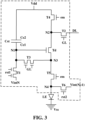
- FIG. 3 is a circuit diagram illustrating the structure of a pixel driving circuit in some embodiments according to the present disclosure.
- the respective pixel driving circuit includes a driving transistor Td; a storage capacitor Cst having a first capacitor electrode Ce1 and a second capacitor electrode Ce2; a first transistor T1 having a gate electrode connected to a respective first reset control signal line of a plurality of first reset control signal line rstl, a source electrode connected to a respective reset signal line VintN in a present stage of a plurality of reset signal line, and a drain electrode connected to a first capacitor electrode Ce1 of the storage capacitor Cst and a gate electrode of the driving transistor Td; a second transistor T2 having a gate electrode connected to a respective gate line of a plurality of gate lines GL, a source electrode connected to a respective data line of a plurality of data lines DL, and a drain electrode connected to a source electrode of the driving transistor Td; a third transistor T
- the third transistor T3 is a "double gate” transistor
- the first transistor T1 is a "double gate” transistor.
- the active layer of the first transistor crosses over a respective reset control signal lines twice (alternatively, the respective reset control signal line crosses over the active layer of the first transistor T1 twice).
- the active layer of the third transistor T3 crosses over a respective gate line of the plurality of gate lines GL twice (alternatively, the respective gate line crosses over the active layer of the third transistor T3 twice).
- the pixel driving circuit further include a first node N1, a second node N2, a third node N3, and a fourth node N4.
- the first node N1 is connected to the gate electrode of the driving transistor Td, the first capacitor electrode Ce1, and the source electrode of the third transistor T3.
- the second node N2 is connected to the drain electrode of the fourth transistor T4, the drain electrode of the second transistor T2, and the source electrode of the driving transistor Td.
- the third node N3 is connected to the drain electrode of the driving transistor Td, the drain electrode of the third transistor T3, and the source electrode of the fifth transistor T5.
- the fourth node N4 is connected to the drain electrode of the fifth transistor T5, the drain electrode of the sixth transistor T6, the drain electrode of the sensing transistor Ts, and the anode of the light emitting element LE.
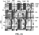
- FIG. 4A is a diagram illustrating the structure of three pixel driving circuits for driving light emission of three light emitting elements of a display panel in some embodiments according to the present disclosure.
- the display panel in some embodiments includes a plurality of gate lines GL respectively extending along a first direction DR1, a plurality of data lines DL respectively extending along a second direction DR2; a plurality of first high voltage signal lines Vdd1 respectively extending along the first direction DR1; a plurality of second high voltage signal lines Vdd2 respectively extending along the second direction DR2; a plurality of first low voltage signal lines Vss1 respectively extending along the first direction DR1; a plurality of second low voltage signal lines Vss2 respectively extending along the second direction DR2; a plurality of first reset signal lines Vint1 respectively extending along the first direction DR1; and a plurality of second reset signal lines Vint2 respectively extending along the second direction DR2.
- the display panel further includes a plurality of first reset control signal lines rst1 respectively extending along the first direction DR1; a plurality of second reset control signal lines rst2 respectively extending along the first direction DR1; and a plurality of light emitting control signal lines em respectively extending along the first direction DR1.
- Corresponding positions of the plurality of transistors in a respective pixel driving circuit are PDC depicted in FIG. 4A .
- the respective pixel driving circuit PDC includes the first transistor T1, the second transistor T2, the third transistor T3, the fourth transistor T4, the fifth transistor T5, the sixth transistor T6, the sensing transistor Ts, and the driving transistor Td.
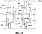
- FIG. 4B is a diagram illustrating the structure of a semiconductor material layer in a display panel depicted in FIG. 4A .
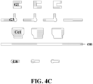
- FIG. 4C is a diagram illustrating the structure of a first conductive layer in a display panel depicted in FIG. 4A .
- FIG. 4D is a diagram illustrating the structure of a second conductive layer in a display panel depicted in FIG. 4A .
- FIG. 4E is a diagram illustrating the structure of a first signal line layer in a display panel depicted in FIG. 4A .
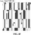
- FIG. 4F is a diagram illustrating the structure of a second signal line layer in a display panel depicted in FIG. 4A .
- FIG. 5A is a cross-sectional view along an A-A' line in FIG.
- the display panel includes a base substrate BS, a semiconductor material layer SML on the base substrate BS, a gate insulating layer GI on a side of the semiconductor material layer SML away from the base substrate BS, a first conductive layer CT1 on a side of the gate insulating layer GI away from the semiconductor material layer SML, an insulating layer IN on a side of the first conductive layer away from the gate insulating layer GI, a second conductive layer CT2 on a side of the insulating layer IN away from the first conductive layer CT1, an inter-layer dielectric layer ILD on a side of the second conductive layer CT2 away from the insulating layer IN, a first signal line layer SL1 on a side of the inter-layer dielectric layer ILD away from the second conductive layer CT2, a planarization layer PLN on a side of the first signal line layer SL1 away from the
- the semiconductor material layer has a unitary structure.
- the respective pixel driving circuit is annotated with labels indicating regions corresponding to the plurality of transistors in the respective pixel driving circuit, including the first transistor T1, the second transistor T2, the third transistor T3, the fourth transistor T4, the fifth transistor T5, the sixth transistor T6, and the driving transistor Td.
- the respective pixel driving circuit is further annotated with labels indicating components of each of the plurality of transistors in the pixel driving circuit.
- the first transistor T1 includes an active layer ACT1, a source electrode S1, and a drain electrode D1.
- the second transistor T2 includes an active layer ACT2, a source electrode S2, and a drain electrode D2.
- the third transistor T3 includes an active layer ACT3, a source electrode S3, and a drain electrode D3.
- the fourth transistor T4 includes an active layer ACT4, a source electrode S4, and a drain electrode D4.
- the fifth transistor T5 includes an active layer ACT5, a source electrode S5, and a drain electrode D5.
- the sixth transistor T6 includes an active layer ACT6, a source electrode S6, and a drain electrode D6.
- the driving transistor Td includes an active layer ACTd, a source electrode Sd, and a drain electrode Dd.
- the active layers (ACT1, ACT2, ACT3, ACT4, ACT5, ACT6, and ACTd) of the transistors (T1, T2, T3, T4, T5, T6, and Td) in the respective pixel driving circuit are parts of a unitary structure.
- the drain electrodes (D1, D2, D3, D4, D5, D6, and Dd) of the transistors (T1, T2, T3, T4, T5, T6, and Td) in the respective pixel driving circuit are parts of a unitary structure.
- the active layers (ACT1, ACT2, ACT3, ACT4, ACT5, ACT6, and ACTd) of the transistors (T1, T2, T3, T4, T5, T6, and Td) are in a same layer.
- the active layers (ACT1, ACT2, ACT3, ACT4, ACT5, ACT6, and ACTd) the source electrodes (S1, S2, S3, S4, S5, S6, Ss, and Sd), and the drain electrodes (D1, D2, D3, D4, D5, D6, and Dd) of the transistors (T1, T2, T3, T4, T5, T6, and Td) are in a same layer.
- the unitary structure of the semiconductor material layer further includes the plurality of first reset signal lines Vint1.
- the plurality of first reset signal lines Vint1 are in a same layer as at least the active layers (e.g., ACT1, ACT2, ACT3, ACT4, ACT5, ACT6, and ACTd) of one or more the transistors (e.g., T1, T2, T3, T4, T5, T6, and Td).
- the active layer refers to a component of the transistor comprising at least a portion of the semiconductor material layer whose orthographic projection on the base substrate overlaps with an orthographic projection of a gate electrode on the base substrate.
- a source electrode refers to a component of the transistor connected to one side of the active layer
- a drain electrode refers to a component of the transistor connected to another side of the active layer.
- the active layer refers to a component of the transistor comprising a first portion of the semiconductor material layer whose orthographic projection on the base substrate overlaps with an orthographic projection of a first gate on the base substrate, a second portion of the semiconductor material layer whose orthographic projection on the base substrate overlaps with an orthographic projection of a second gate on the base substrate, and a third portion between the first portion and the second portion.
- a source electrode refers to a component of the transistor connected to a side of the first portion distal to the third portion
- a drain electrode refers to a component of the transistor connected to a side of the second portion distal to the third portion.
- the first conductive layer in some embodiments includes a gate electrode G1 of the first transistor T1, a gate electrode G3 of the third transistor T3, a gate electrode G6 of the sixth transistor T6, a plurality of light emitting control signal lines em, and a first capacitor electrode Ce1 of the storage capacitor Cst.
- a conductive material may be deposited on the substrate by a plasma-enhanced chemical vapor deposition (PECVD) process and patterned.
- PECVD plasma-enhanced chemical vapor deposition
- Examples of appropriate conductive materials for making the first conductive layer include, but are not limited to, aluminum, copper, molybdenum, chromium, aluminum copper alloy, copper molybdenum alloy, molybdenum aluminum alloy, aluminum chromium alloy, copper chromium alloy, molybdenum chromium alloy, copper molybdenum aluminum alloy, and the like.
- the gate electrode G1 of the first transistor T1, the gate electrode G3 of the third transistor T3, the gate electrode G6 of the sixth transistor T6, the plurality of light emitting control signal lines em, and the first capacitor electrode Ce1 are in a same layer.
- the term “same layer” refers to the relationship between the layers simultaneously formed in the same step.
- the plurality of light emitting control signal lines em and the first capacitor electrode Ce1 are in a same layer when they are formed as a result of one or more steps of a same patterning process performed in a same layer of material.
- the plurality of light emitting control signal lines em and the first capacitor electrode Ce1 can be formed in a same layer by simultaneously performing the step of forming the plurality of light emitting control signal lines em, and the step of forming the first capacitor electrode Ce1.
- the term “same layer” does not always mean that the thickness of the layer or the height of the layer in a cross-sectional view is the same.
- a respective gate line of the plurality of gate lines comprises a plurality of metal blocks (e.g., G3 in FIG. 4C ) spaced apart from each other in a first conductive layer, and a metal line (e.g., GL in FIG. 4E ) along a first direction in the first signal line layer.
- the metal line along the first direction is connected to the plurality of metal blocks, respectively.
- the metal line in the first signal line layer can be made with a metallic material having a relatively low resistance, as compared to the metallic material in the first conductive layer. By having this design, the overall resistance of the gate line can be lowered.
- the second conductive layer in some embodiments includes a second capacitor electrode Ce2 of the storage capacitor Cst.
- a conductive material may be deposited on the substrate by a plasma-enhanced chemical vapor deposition (PECVD) process and patterned.
- PECVD plasma-enhanced chemical vapor deposition
- Examples of appropriate conductive materials for making the second conductive layer include, but are not limited to, aluminum, copper, molybdenum, chromium, aluminum copper alloy, copper molybdenum alloy, molybdenum aluminum alloy, aluminum chromium alloy, copper chromium alloy, molybdenum chromium alloy, copper molybdenum aluminum alloy, and the like.
- the first signal line layer in some embodiments includes a plurality of first low voltage signal lines Vss1, a plurality of first reset control signal lines rstl, a plurality of gate lines GL, a plurality of first high voltage signal lines Vdd1, a plurality of second reset control signal lines rst2, and a node connecting line Cln.
- the node connecting line Cln connects the first capacitor electrode Ce1 and the source electrode S3 of the third transistor T3 in a respective pixel driving circuit together.
- Various appropriate conductive materials and various appropriate fabricating methods may be used to make the first signal line layer.
- a conductive material may be deposited on the substrate by a plasma-enhanced chemical vapor deposition (PECVD) process and patterned.
- PECVD plasma-enhanced chemical vapor deposition
- appropriate conductive materials for making the first signal line layer include, but are not limited to, aluminum, copper, molybdenum, chromium, aluminum copper alloy, copper molybdenum alloy, molybdenum aluminum alloy, aluminum chromium alloy, copper chromium alloy, molybdenum chromium alloy, copper molybdenum aluminum alloy, and the like.
- the plurality of first low voltage signal lines Vss1, the plurality of first reset control signal lines rstl, the plurality of gate lines GL, the plurality of first high voltage signal lines Vdd1, the plurality of second reset control signal lines rst2, and the node connecting line Cln are in a same layer.
- the respective first reset control signal line rst1 include a plurality of first metal blocks spaced apart from each other in a first conductive layer, and a first metal line along a first direction in the first signal line layer, the first metal line along the first direction being connected to the plurality of first metal blocks, respectively.
- the respective second reset control signal line comprises a plurality of second metal blocks spaced apart from each other in the first conductive layer, and a second metal line along the first direction in the first signal line layer, the second metal line along the first direction being connected to the plurality of second metal blocks, respectively.
- a respective first low voltage signal line of a plurality of first low voltage signal lines Vss1 includes a first linear portion, a second linear portion, and a connecting portion connecting the first linear portion and the second linear portion.
- a virtual extension of the first linear portion crosses over the plurality of first metal blocks (e.g., G1 in FIG. 4C ) of the respective first reset control signal line rstl.
- a virtual extension of the second linear portion is spaced apart from the plurality of first metal blocks, e.g., does not cross over the plurality of first metal blocks (e.g., G1 in FIG. 4C ) of the respective first reset control signal line rstl.
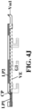
- FIG. 4J is a diagram illustrating a relative position between a respective one of a plurality of first low voltage signal lines and a plurality of first metal blocks of a respective first reset control signal line in some embodiments according to the present disclosure.
- a respective first low voltage signal line of a plurality of first low voltage signal lines Vss1 includes a first linear portion LP1, a second linear portion LP2, and a connecting portion CP connecting the first linear portion LP1 and the second linear portion LP2.
- a virtual extension VE of the first linear portion LP1 crosses over the plurality of first metal blocks (G1) of the respective first reset control signal line rstl.
- a virtual extension of the second linear portion LP2 is spaced apart from the plurality of first metal blocks, e.g., does not cross over the plurality of first metal blocks (G1) of the respective first reset control signal line rstl.
- the second signal line layer in some embodiments includes a plurality of data line DL, a plurality of second low voltage signal lines Vss2, a plurality of second reset signal lines Vint2, and a plurality of second high voltage signal lines Vdd2.
- Various appropriate conductive materials and various appropriate fabricating methods may be used to make the second signal line layer.
- a conductive material may be deposited on the substrate by a plasma-enhanced chemical vapor deposition (PECVD) process and patterned.
- PECVD plasma-enhanced chemical vapor deposition
- Examples of appropriate conductive materials for making the second signal line layer include, but are not limited to, aluminum, copper, molybdenum, chromium, aluminum copper alloy, copper molybdenum alloy, molybdenum aluminum alloy, aluminum chromium alloy, copper chromium alloy, molybdenum chromium alloy, copper molybdenum aluminum alloy, and the like.
- the plurality of data line DL, the plurality of second low voltage signal lines Vss2, the plurality of second reset signal lines Vint2, and the plurality of second high voltage signal lines Vdd2 are in a same layer.
- a minimal distance between a respective second reset signal line of the plurality of second reset signal lines Vint2 and a respective second low voltage signal line of the plurality of second low voltage signal lines Vss2 that is most adjacent to the respective second reset signal line is less than a minimal distance between the respective second reset signal line and a respective data line of a plurality of data lines DL that is most adjacent to the respective second reset signal line.
- a total of three data lines and a total of one second low voltage signal line are between two most adjacent second reset signal lines of the plurality of second reset signal lines Vint2.
- a total of three data lines, a total of one second low voltage signal line, and a total of three second high voltage signal lines are between two most adjacent second reset signal lines of the plurality of second reset signal lines Vint2.
- an orthographic projection of the second capacitor electrode Ce2 on a base substrate BS completely covers, with a margin, an orthographic projection of the first capacitor electrode Ce1 on the base substrate BS except for a hole region H in which a portion of the second capacitor electrode Ce2 is absent.
- the first signal line layer includes a node connecting line Cln on a side of the inter-layer dielectric layer ILD away from the second capacitor electrode Ce2.
- the node connecting line Cln is in a same layer as the plurality of first low voltage signal lines Vss1, the plurality of first reset control signal lines rstl, the plurality of gate lines GL, the plurality of first high voltage signal lines Vdd1, and the plurality of second reset control signal lines rst2.
- the display panel further includes a first connecting via cv1 in the hole region H and extending through the inter-layer dielectric layer ILD and the insulating layer IN.
- the node connecting line Cln is connected to the first capacitor electrode Ce1 through the first connecting via cv1.
- the first capacitor electrode Ce1 is on a side of the gate insulating layer IN away from the base substrate BS.
- the display panel further includes a first connecting via cv1 and a second connecting via cv2.
- the first connecting via cv1 is in the hole region H and extends through the inter-layer dielectric layer ILD and the insulating layer IN.
- the second connecting via cv2 extends through the inter-layer dielectric layer ILD, the insulating layer IN, and the gate insulating layer GI.
- the node connecting line Cln is connected to the first capacitor electrode Ce1 through the first connecting via cv1, and the node connecting line Cln is connected to the semiconductor material layer SML through the second connecting via cv2.
- the node connecting line Cln is connected to the source electrode S3 of third transistor T3, as depicted in FIG. 5A .
- the second capacitor electrode Ce2 includes an extension E extending away from an electrode main body emb of the second capacitor electrode Ce2.
- an orthographic projection of the extension E on a base substrate at least partially overlaps with an orthographic projection of an active layer of a third transistor T3 of the respective pixel driving circuit on the base substrate.
- a portion of the extension E is between a first node N1 of the respective pixel driving circuit and a respective data line of the plurality of data lines dl, configured to prevent interference from signals passing through the respective data line to the first node N1.
- FIG. 6A is a diagram illustrating the structure of an interconnected low voltage supply network, an interconnected reset signal supply network, and an interconnected high voltage supply network in a display panel in some embodiments according to the present disclosure.
- the interconnected low voltage supply network includes signal lines in a display area of the display panel.
- the interconnected low voltage supply network is configured to provide a low voltage signal to cathodes of the plurality of light emitting elements.
- the interconnected reset signal supply network is configured to provide a reset signal to a plurality of pixel driving circuits.
- the interconnected reset signal supply network includes signal lines in a display area of the display panel.
- the interconnected high voltage supply network is configured to provide a high voltage signal to a plurality of pixel driving circuits.
- the interconnected high voltage supply network includes signal lines in a display area of the display panel. In one example, a first voltage signal line is a low voltage signal line, and a second voltage signal line is a high voltage signal line.
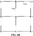
- FIG. 6B is a diagram illustrating the structure of an interconnected low voltage supply network in a display panel in some embodiments according to the present disclosure.
- the interconnected low voltage supply network in some embodiments includes a plurality of first low voltage signal lines Vss1 respectively along a first direction DR1; and a plurality of second low voltage signal lines Vss2 respectively along a second direction DR2.
- the plurality of first low voltage signal lines Vss1 respectively cross over the plurality of second low voltage signal lines Vss2.
- a respective one of the plurality of first low voltage signal lines Vss1 is connected to at least multiple ones of the plurality of second low voltage signal lines Vss2.
- a respective one of the plurality of second low voltage signal lines Vss2 is connected to at least multiple ones of the plurality of first low voltage signal lines Vss1.
- FIG. 5B is a cross-sectional view along a B-B' line in FIG. 4A .
- the first signal line layer SL1 includes the plurality of first low voltage signal lines Vss1
- the second signal line layer SL2 includes the plurality of second low voltage signal lines Vss2.
- the plurality of first low voltage signal lines Vss1 and the plurality of second low voltage signal lines Vss2 interconnect through first vias v1s respectively extending through the planarization layer PLN. At least some of the first vias are in the display area.
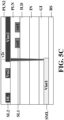
- FIG. 5C is a cross-sectional view along a C-C' line in FIG. 4A .
- the semiconductor material layer SML includes the plurality of first reset signal lines Vint1
- the second signal line layer SL2 includes the plurality of second reset signal lines Vint2.
- the plurality of first reset signal lines Vint1 and the plurality of second reset signal lines Vint2 interconnect through second vias v2s respectively extending through at least the planarization layer PLN.
- the plurality of first reset signal lines Vint1 include a semiconductor material; and the plurality of second reset signal lines Vint2 include a metallic material.
- the plurality of first reset signal lines Vint1 and at least active layers (e.g., ACTd, and ACT1 to ACT6) of a plurality of thin film transistors (e.g., Td, and T1 to T6) are in the semiconductor material layer SML, and include a same semiconductor material.
- the reset signal lines may be disposed in the first conductive layer.
- the reset signal lines (one or both of the plurality of first reset signal lines Vint1 and the plurality of second reset signal lines Vint2) may be disposed in the first signal line layer.
- the reset signal lines (one or both of the plurality of first reset signal lines Vint1 and the plurality of second reset signal lines Vint2) may be disposed in the second conductive layer.
- the reset signal lines (one or both of the plurality of first reset signal lines Vint1 and the plurality of second reset signal lines Vint2) may be disposed in the second signal line layer.
- the plurality of first reset signal lines Vint1 and the plurality of second reset signal lines Vint2 are in a same layer, interconnecting with each other to form a network.
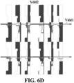
- FIG. 6D is a diagram illustrating the structure of an interconnected high voltage supply network in a display panel in some embodiments according to the present disclosure.
- the interconnected high voltage supply network in some embodiments includes a plurality of first high voltage signal lines Vdd1 respectively along a first direction DR1; and a plurality of second high voltage signal lines Vdd2 respectively along a second direction DR2.
- the plurality of first high voltage signal lines Vdd1 respectively cross over the plurality of second high voltage signal lines Vdd2.
- a respective one of the plurality of first high voltage signal lines Vdd1 is connected to at least multiple ones of the plurality of second high voltage signal lines Vdd2.
- a respective one of the plurality of second high voltage signal lines Vdd2 is connected to at least multiple ones of the plurality of first high voltage signal lines Vdd1.
- FIG. 5D is a cross-sectional view along a D-D' line in FIG. 4A .
- the first signal line layer SL1 includes the plurality of first high voltage signal lines Vdd1
- the second signal line layer SL2 includes the plurality of second high voltage signal lines Vdd2.
- a respective one of the plurality of first high voltage signal lines Vdd1 is connected to second capacitor electrode through one or more third vias v3s respectively extending through the inter-layer dielectric layer ILD.
- a respective one of the plurality of first high voltage signal lines Vdd1 is connected to at least multiple ones of the plurality of second high voltage signal lines Vdd2 respectively through multiple third vias extending through the planarization layer PLN.
- a respective one of the plurality of second high voltage signal lines Vdd2 is connected to at least multiple ones of the plurality of first high voltage signal lines Vdd1 respectively through multiple third vias extending through the planarization layer PLN.
- FIG. 5E is a cross-sectional view along an E-E' line in FIG. 4A .
- the first signal line layer SL1 includes the plurality of first high voltage signal lines Vdd1
- the second signal line layer SL2 includes the plurality of second high voltage signal lines Vdd2.
- a respective one of the plurality of first high voltage signal lines Vdd1 is connected to second capacitor electrode through one or more third vias v3s respectively extending through the inter-layer dielectric layer ILD.
- a respective one of the plurality of second high voltage signal line Vdd2 is connected to a respective one of the plurality of first high voltage signal lines Vdd1 through one or more fourth vias v4s respectively extending through the planarization layer PLN.
- a respective one of the plurality of first high voltage signal lines Vdd1 is connected to the source electrode S4 of the fourth transistor through a third connecting via cv4 extending through the inter-layer dielectric layer ILD, the insulating layer IN, and the gate insulating layer GI.
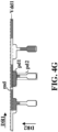
- FIG. 4G is a diagram illustrating the structure of a respective one of a plurality of first high voltage signal lines in some embodiments according to the present disclosure.
- the respective one of a plurality of first high voltage signal lines Vdd1 in some embodiments includes a main body md extending along the first direction DR1, a first protrusion pd1 protruding away from the main body md along the second direction DR2, and a second protrusion pd2 protruding away from the first protrusion pd1 along the second direction DR2.
- the second protrusion pd2 connects to the main body md through the first protrusion pd1.
- the first protrusion pd1 is a portion of the respective one of a plurality of first high voltage signal lines Vdd1 where the respective one of a plurality of first high voltage signal lines Vdd1 connects to the second capacitor electrode.
- the second protrusion pd2 is a portion of the respective one of a plurality of first high voltage signal lines Vdd1 where the respective one of a plurality of first high voltage signal lines Vdd1 connects to the source electrode of the fourth transistor.
- a drain electrode of the fourth transistor is connected to a source electrode of a driving transistor.
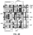
- FIG. 4H is a diagram illustrating the layout of anodes of light emitting elements with respect to pixel driving circuits of a display panel in some embodiments according to the present disclosure.
- FIG. 4I is a diagram illustrating the structure of anodes, a first signal line layer, and a second signal line layer in a display panel in some embodiments according to the present disclosure.
- the display panel in some embodiments further includes a plurality of anodes respectively of the plurality of light emitting elements, for example, a first anode AD1, a second anode AD2, and a third anode AD3 as depicted in FIG. 4H .
- a respective anode is connected to an anode contact pad through a via extending through a second planarization layer (e.g., PLN2 in FIG. 5A to FIG. 5E ), and the anode contact pad is connected to a relay electrode through a via extending through the planarization layer (e.g., PLN in FIG. 5A to FIG. 5E ).
- the relay electrode is connected to the N4 node (e.g., the drain electrode of the fifth transistor) through a via extending through the inter-layer dielectric layer.
- the first anode AD1 is connected to a first anode contact pad ACP1 through a via extending through the second planarization layer, the first anode contact pad ACP1 is connected to a first relay electrode RE1 through a via extending through the planarization layer;
- the second anode AD2 is connected to a second anode contact pad ACP2 through a via extending through the second planarization layer, the second anode contact pad ACP2 is connected to a second relay electrode RE2 through a via extending through the planarization layer;
- the third anode AD3 is connected to a third anode contact pad ACP3 through a via extending through the second planarization layer, the third anode contact pad ACP3 is connected to a third relay electrode RE3 through a via extending through the planarization layer.
- the display panel further includes a gate-on-array circuit GOA in a peripheral area PA of the display panel.
- the interconnected low voltage supply network VSSN includes a first peripheral low voltage line pvss1 in the peripheral area PA on a first side S1 of the display panel.
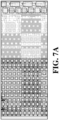
- FIG. 7A is a schematic diagram illustrating the structure in a first zoom-in region ZR1 in FIG. 1 .
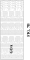
- FIG. 7B is a diagram illustrating the structure of a first signal line layer in a first region ZR1 depicted in FIG. 7A .
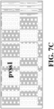
- FIG. 7C is a diagram illustrating the structure of a second signal line layer in a first region ZR1 depicted in FIG. 7A .
- FIG. 7D is a diagram illustrating the structure of a second planarization layer in a first region ZR1 depicted in FIG. 7A .
- FIG. 7E is a diagram illustrating the structure of an anode layer in a first region ZR1 depicted in FIG. 7A .
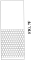
- FIG. 7F is a diagram illustrating the structure of a third planarization layer in a first region ZR1 depicted in FIG. 7A .
- FIG. 7G is a diagram illustrating the structure of a cathode layer in a first region ZR1 depicted in FIG. 7A . Referring to FIG. 7A to FIG. 7G , and FIG.
- the display panel in the peripheral area PA on the first side S1 of the display panel include a gate-on-array circuit GOA in the first signal line layer on a base substrate, a first peripheral low voltage line pvss1 in the second signal line layer on a side of the gate-on-array circuit GOA away from the base substrate, a second planarization layer PLN2 on a side of the first peripheral low voltage line pvss1 away from the gate-on-array circuit GOA, an anode metal layer AML in an anode layer on a side of the second planarization layer PLN2 away from the first peripheral low voltage line pvss1, a third planarization layer PLN3 on a side of the anode metal layer AML away from the second planarization layer PLN2, and a cathode layer CDL on a side of the third planarization layer PLN3 away from the anode metal layer AML.
- FIG. 8 is a cross-sectional view along an F-F' line in FIG. 7A .
- an orthographic projection of the first peripheral low voltage line pvss1 on a base substrate BS at least partially overlaps with an orthographic projection of the gate-on-array circuit GOA on the base substrate BS.
- the orthographic projection of the first peripheral low voltage line pvss1 on a base substrate BS at least 80% (e.g., at least 85%, at least 90%, at least 95%, at least 99%) overlaps with the orthographic projection of the gate-on-array circuit GOA on the base substrate BS.
- the cathode layer CDL is connected to the anode metal layer AML through one or more first peripheral vias pv1 in the peripheral area and extending through a third planarization layer PLN3, and the anode metal layer AML is connected to the first peripheral first voltage line pvss1 through one or more second peripheral vias pv2 in the peripheral area and extending through a second planarization layer PLN2, thereby providing the first voltage signal to the cathodes of the plurality of light emitting elements.
- the display panel includes a plurality of first gas releasing vias grv1 extending through the first peripheral first voltage line pvss1 for releasing gases in underneath insulating layer (e.g., the planarization layer PLN) during a fabrication process of the display panel.
- the display panel further includes a plurality of second gas releasing vias grv2 extending through the anode metal layer AML for releasing gases in underneath insulating layer (e.g., the second planarization layer PLN2) during a fabrication process of the display panel.
- the cathode layer CDL is a unitary cathode layer extending substantially throughout the display panel and functions as cathodes for the plurality of light emitting elements.
- the one or more vias connecting the cathode layer CDL and the anode metal layer AML are limited in the peripheral area PA, and absent in the display area DA.
- the cathode layer CDL is connected to the interconnected low voltage supply network VSSN only through the anode metal layer AML.
- the low voltage line shares a same space as the gate-on-array circuit GOA.
- the display panel can be made with a very narrow bezel.
- the present display panel has a bezel width on the first side S1 (or the side opposite to the first side S1) of approximately 1.5 mm, as compared to 2.5 mm in a related display panel.
- the connection between the low voltage line and the cathode layer CDL (through the anode metal layer) is made exclusively in the peripheral area PA (e.g., in the GOA region), obviating the need of making vias (or any process at all) in the display area DA to connect the low voltage line and the cathode layer CDL.
- the display panel can be fabricated with much less complexity, significantly lowering occurrence of defects in the display panel.
- FIG. 9A shows an IR drop in a display panel in some embodiments according to the present disclosure.
- FIG. 9B shows an IR drop in a related display panel without an interconnected low voltage supply network.
- a degree of darkness indicates a degree of IR drop in a local region. Comparing FIG. 9A and FIG. 9B , the degree of voltage drop in the embodiments according to the present disclosure is dramatically reduced as compared to the degree of voltage drop in the related display panel without an interconnected low voltage supply network.
- the IR drop is reduced from 1.5641 V to 1.2337 V (more than 20% reduction).
- the advantages of the present display panel are particularly meaningful for large size display panels.
- the VSS current concentrates at outmost two ports, leading to issues such as high current burns.
- the VSS current at the outmost port is about 26.6% of the total VSS current.
- the VSS current at any port is less than 11% of the total VSS current, obviating the issue of large current burns.
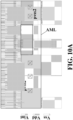
- FIG. 10A is a schematic diagram illustrating the structure in a second zoom-in region ZR2 in FIG. 1 .
- FIG. 10B is a schematic diagram illustrating the structure of low voltage signal lines in FIG. 10A .
- FIG. 10C is a schematic diagram illustrating the structure of high voltage signal lines in FIG. 10A . Referring to FIG. 1 , FIG. 10A , FIG. 10B , and FIG.
- the display panel includes a peripheral high voltage signal line pvdd, a second peripheral low voltage signal line pvss2, and a third peripheral low voltage signal line pvss3 in the peripheral area PA on a second side S2 of the display panel.
- One or more of the plurality of second high voltage signal lines Vdd2 are connected to the peripheral high voltage signal line pvdd.
- One or more of the plurality of second low voltage signal lines Vss2 are connected to the second peripheral low voltage signal line pvss2.
- the second peripheral low voltage signal line pvss2 and the third peripheral low voltage signal line pvss3 are connected to each other through a plurality of bridges bg.
- the plurality of first low voltage signal lines, the peripheral high voltage signal line pvdd, and the plurality of bridges are in a first signal line layer SL1 (referring to, e.g., FIG. 5A for layer arrangement of the display panel).
- the plurality of second high voltage signal lines Vdd2, the second peripheral low voltage signal line pvss2 are in a second signal line layer SL2.
- the third peripheral low voltage signal line pvss3 includes a first sub-layer in the first signal line layer SL1 and a second sub-layer in the second signal line layer SL2.
- FIG. 10D is a schematic diagram illustrating the structure of reset signal lines in FIG. 10A .
- the display panel includes a peripheral reset signal line pvint in the peripheral area PA on a second side S2 of the display panel.
- One or more of the plurality of second reset signal lines Vint2 are connected to the peripheral reset signal line pvint.
- the peripheral reset signal line pvint is in a layer different from the peripheral high voltage signal line pvdd and the peripheral low voltage signal line pvss2.
- the peripheral reset signal line pvint is in a same layer as the plurality of second reset signal lines Vint2.
- the peripheral reset signal line pvint is in a layer different from the plurality of second reset signal lines Vint2.
- the peripheral reset signal line pvint includes a first part p1 and a second part p2.
- the first part p1 includes a single layer conductive material in a same layer as the second signal line layer.
- the second part has a double-layer structure including conductive materials respectively in the first signal line layer and the second signal line layer.
- the display panel further include an anode metal layer AML.
- the anode metal layer AML is connected to the peripheral low voltage signal line pvss2 through vias extending through one or more insulating layers.
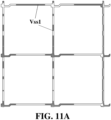
- FIG. 11A is a diagram illustrating the structure of a first sub-network of an interconnected low voltage supply network in some embodiments according to the present disclosure.
- FIG. 11B is a diagram illustrating the structure of a second sub-network of an interconnected low voltage supply network in some embodiments according to the present disclosure.
- FIG. 11 C is a diagram illustrating the structure of an interconnected low voltage supply network comprising a first sub-network and a second sub-network in some embodiments according to the present disclosure.
- the interconnected low voltage supply network in some embodiments includes a first sub-network formed by the plurality of first low voltage signal lines Vss1 and a second sub-network formed by the plurality of second low voltage signal lines Vss2.
- the first sub-network is in the first signal line layer and the second sub-network is in the second signal line layer.
- the plurality of first signal lines Vss1 are electrically connected to the plurality of second signal lines Vss2.
- the plurality of first low voltage signal lines Vss1 form a sub-network whereas the plurality of second low voltage signal lines Vss2 do not form a sub-network. In some embodiments, the plurality of second low voltage signal lines Vss2 form a sub-network whereas the plurality of first low voltage signal lines Vss1 do not form a sub-network.
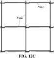
- FIG. 12A is a diagram illustrating the structure of a plurality of first low voltage signal lines of an interconnected low voltage supply network in some embodiments according to the present disclosure.
- FIG. 12B is a diagram illustrating the structure of a sub-network of a plurality of second low voltage signal lines of an interconnected low voltage supply network in some embodiments according to the present disclosure.
- FIG. 12C is a diagram illustrating the structure of an interconnected low voltage supply network comprising a plurality of first low voltage signal lines and a sub-network of a plurality of second low voltage signal lines in some embodiments according to the present disclosure. Referring to FIG. 12A to FIG.
- the plurality of first low voltage signal lines Vss1 are separated from each other and does not form a sub-network, whereas the plurality of second low voltage signal lines Vss2 form a sub-network.
- the plurality of first signal lines Vss1 are electrically connected to the plurality of second signal lines Vss2.
- the present invention provides a display apparatus, including the display panel described herein or fabricated by a method described herein, and one or more integrated circuits connected to the display panel.
- display apparatuses include, but are not limited to, an electronic paper, a mobile phone, a tablet computer, a television, a monitor, a notebook computer, a digital album, a GPS, etc.
- the display apparatus is an organic light emitting diode display apparatus.
- the display apparatus is a liquid crystal display apparatus.
- the present disclosure provides a method of fabricating a display panel.
- the method includes forming a plurality of light emitting elements; and forming an interconnected low voltage supply network configured to provide a low voltage signal to cathodes of the plurality of light emitting elements.
- forming the interconnected low voltage supply network includes forming signal lines in a display area of the display panel.
- the term "the invention”, “the present invention” or the like does not necessarily limit the claim scope to a specific embodiment, and the reference to exemplary embodiments of the invention does not imply a limitation on the invention, and no such limitation is to be inferred.
- the invention is limited only by the scope of the appended claims. Moreover, these claims may refer to use "first”, “second”, etc. following with noun or element. Such terms should be understood as a nomenclature and should not be construed as giving the limitation on the number of the elements modified by such nomenclature unless specific number has been given. Any advantages and benefits described may not apply to all embodiments of the invention.
Landscapes
- Engineering & Computer Science (AREA)
- Microelectronics & Electronic Packaging (AREA)
- Physics & Mathematics (AREA)
- Computer Hardware Design (AREA)
- General Physics & Mathematics (AREA)
- Theoretical Computer Science (AREA)
- Devices For Indicating Variable Information By Combining Individual Elements (AREA)
- Electroluminescent Light Sources (AREA)
- Control Of El Displays (AREA)
Claims (14)
- Panneau d'affichage comprenant une pluralité de sous-pixels, chaque sous-pixel comprenant un élément luminescent et un circuit de commande de pixel ;
dans lequel le panneau d'affichage comprend :un substrat de base (BS) ;une pluralité d'éléments luminescents ; etun premier réseau d'alimentation en tension interconnecté, configuré pour fournir un premier signal de tension aux cathodes de la pluralité d'éléments luminescents ;dans lequel le premier réseau d'alimentation en tension interconnecté comprend des lignes de signaux dans une zone d'affichage (DA) du panneau d'affichage, la zone d'affichage (DA) étant au moins partiellement entourée d'une zone périphérique (PA) ;les lignes de signaux comprennent une pluralité de premières lignes de signaux dans une première couche de lignes de signaux (SL1) et une pluralité de deuxièmes lignes de signaux dans une deuxième couche de lignes de signaux (SL2) ;le panneau d'affichage comprend en outre une couche de planarisation (PLN) entre la première couche de lignes de signaux (SL1) et la deuxième couche de lignes de signaux (SL2) ; etla pluralité de premières lignes de signaux est connectée électriquement à la pluralité de deuxièmes lignes de signaux,caractérisé en ce que,le panneau d'affichage comprend en outre : un circuit à matrice de porte (GOA) dans la zone périphérique (PA) du panneau d'affichage ; une couche métallique anodique (AML) sur un côté d'une première ligne de tension périphérique (pvss1) du premier réseau d'alimentation en tension interconnecté, loin du circuit à matrice de porte (GOA) ; et une couche cathodique (CDL) sur un côté de la couche métallique anodique (AML), loin de la première ligne de tension périphérique (pvss1) ;dans lequel la première ligne de tension périphérique (pvss1) se trouve dans la zone périphérique (PA) d'un premier côté (S1) du panneau d'affichage ; etune projection orthographique de la première ligne de tension périphérique (pvss1) sur le substrat de base (BS) chevauche au moins partiellement une projection orthographique du circuit à matrice de porte (GOA) sur le substrat de base (BS), etdans lequel la couche cathodique (CDL) est connectée à la couche métallique anodique (AML) par un ou plusieurs premiers passages périphériques (pv1) dans la zone périphérique et s'étendant à travers une troisième couche de planarisation (PLN3), et la couche métallique anodique (AML) est connectée à la première ligne de tension périphérique (pvss1) à travers un ou plusieurs deuxièmes passages périphériques (pv2) dans la zone périphérique et s'étendant à travers une deuxième couche de planarisation (PLN2), fournissant ainsi le premier signal de tension aux cathodes de la pluralité d'éléments luminescents ;le ou les premiers passages périphériques reliant la couche cathodique (CDL) et la couche métallique anodique (AML), et le ou les deuxièmes passages périphériques reliant la couche métallique anodique (AML) et le premier réseau d'alimentation en tension interconnecté sont limités dans la zone périphérique (PA), et absents dans la zone d'affichage (DA) ; etla première ligne de tension périphérique (pvss1) et la couche métallique anodique (AML) connectée à la première ligne de tension périphérique (pvss1) entourent respectivement partiellement la zone d'affichage (DA). - Panneau d'affichage selon la revendication 1, dans lequel le premier réseau d'alimentation en tension interconnecté comprend :une pluralité de premières premières lignes de signaux de tension (Vss1) respectivement le long d'une première direction (DR1) ; etune pluralité de secondes premières lignes de signaux de tension (Vss2), respectivement le long d'une deuxième direction (DR2) ;dans lequel la pluralité de premières premières lignes de signaux de tension (Vss1) croise respectivement la pluralité de deuxièmes premières lignes de signaux de tension (Vss2), et dans lequel, éventuellement, le premier réseau d'alimentation en tension interconnecté comprend un premier sous-réseau formé par la pluralité de premières premières lignes de signaux de tension (Vss1) et un deuxième sous-réseau formé par la pluralité de deuxièmes premières lignes de signaux de tension (Vss2).
- Panneau d'affichage selon la revendication 2, dans lequel une ligne respective de la pluralité de premières premières lignes de signaux de tension (Vss1) est connectée à au moins plusieurs deuxièmes premières lignes de signal de deuxième tension (Vss2), et une ligne respective de la pluralité de deuxièmes premières lignes de signaux de tension (Vss2) est connectée à au moins plusieurs premières premières lignes de signaux de tension (Vss1) ; et éventuellement, la pluralité de premières premières lignes de signaux de tension (Vss1) et la pluralité de deuxièmes premières lignes de signaux de tension (Vss2) sont interconnectées par des premiers passages (v1s) s'étendant respectivement à travers la couche de planarisation (PLN), au moins certains des premiers passages (v1s) se trouvant dans la zone d'affichage (DA) ;une ligne respective de la pluralité de premières premières lignes de signaux de tension (Vss1) est connectée à au moins plusieurs deuxièmes premières lignes de signaux de tension (Vss2) respectivement à travers plusieurs premiers passages s'étendant à travers la couche de planarisation (PLN) ; etune ligne respective de la pluralité de deuxièmes premières lignes de signaux de tension (Vss2) est connectée à au moins plusieurs lignes de la pluralité de premières premières lignes de signaux de tension (Vss1) respectivement à travers plusieurs premiers passages s'étendant à travers la couche de planarisation (PLN).
- Panneau d'affichage selon l'une quelconque des revendications 1 à 3 comprend en outre un réseau interconnecté d'alimentation en signaux de réinitialisation configuré pour fournir un signal de réinitialisation à une pluralité de circuits de commande de pixels ;
dans lequel le réseau interconnecté d'alimentation en signaux de réinitialisation comprend des lignes de signaux dans la zone d'affichage (DA) du panneau d'affichage. - Panneau d'affichage selon la revendication 4, dans lequel le réseau interconnecté d'alimentation en signaux de réinitialisation comprend :une pluralité de premières lignes de signaux de réinitialisation (Vint1) respectivement le long d'une première direction (DR1) ; etune pluralité de deuxièmes lignes de signaux de réinitialisation (Vint2) respectivement le long d'une deuxième direction (DR2) ;dans lequel la pluralité de premières lignes de signaux de réinitialisation (Vint1) croise respectivement la pluralité de deuxièmes lignes de signaux de réinitialisation (Vint2),une ligne respective de la pluralité de premières lignes de signaux de réinitialisation (Vint1) est connectée à au moins plusieurs lignes de la pluralité de deuxièmes lignes de signaux de réinitialisation (Vint2) ; etune ligne respective de la pluralité de deuxièmes lignes de signaux de réinitialisation (Vint2) est connectée à au moins plusieurs lignes de la pluralité de premières lignes de signaux de réinitialisation (Vint1).
- Panneau d'affichage selon la revendication 5, dans lequel une distance minimale entre une deuxième ligne de signaux de réinitialisation respective de la pluralité de deuxième lignes de signaux de réinitialisation (Vint2) et une deuxième première ligne de signaux de tension respective de la pluralité de deuxièmes premières lignes de signaux de tension (Vss2) qui est la plus adjacente à la deuxième ligne de signaux de réinitialisation respective est inférieure à une distance minimale entre la deuxième ligne de signaux de réinitialisation respective et une ligne de données respective d'une pluralité de lignes de données (DL) qui est la plus adjacente à la deuxième ligne de signaux de réinitialisation respective, et dans lequel un total de trois lignes de données et un total d'une deuxième première ligne de signaux de tension se trouvent entre les deux deuxièmes lignes de signaux de réinitialisation les plus adjacentes de la pluralité de deuxièmes lignes de signaux de réinitialisation (Vint2).
- Panneau d'affichage selon l'une quelconque des revendications 1 à 6, comprenant :une couche de matériau semi-conducteur (SML) sur le substrat de base (BS) ;une couche de planarisation (PLN) sur une face de la couche de matériau semi-conducteur (SML) éloignée du substrat de base (BS) ; etla deuxième couche de ligne de signaux (SL2) sur une face de la couche de planarisation (PLN) éloignée de la couche de matériau semi-conducteur (SML) ;dans lequel le panneau d'affichage comprend en outre un réseau interconnecté d'alimentation en signaux de réinitialisation configuré pour fournir un signal de réinitialisation à une pluralité de circuits de commande de pixels ;le réseau interconnecté d'alimentation en signaux de réinitialisation comprend une pluralité de premières lignes de signaux de réinitialisation (Vint1) respectivement le long d'une première direction (DR1) et une pluralité de deuxièmes lignes de signaux de réinitialisation (Vint2) respectivement le long d'une deuxième direction (DR2) ; etla couche de matériau semi-conducteur (SML) comprend la pluralité de premières lignes de signaux de réinitialisation (Vint1), et la deuxième couche de ligne de signaux (SL2) comprend la pluralité de deuxièmes lignes de signaux de réinitialisation (Vint2).
- Panneau d'affichage selon la revendication 7, dans lequel la pluralité de lignes de signaux de réinitialisation (Vint1) et la pluralité de lignes de signaux de réinitialisation (Vint2) s'interconnectent par l'intermédiaire de deuxièmes passages (v2s) s'étendant respectivement à travers au moins la couche de planarisation (PLN) ;
dans lequel le panneau d'affichage comprend en outre :une couche isolante de grille (GI) sur une face de la couche de matériau semi-conducteur (SML) éloignée du substrat de base (BS) ;une couche isolante (IN) sur une face de la couche isolante de grille (GI) éloignée de la couche de matériau semi-conducteur (SML) ; etune couche diélectrique intercouche (ILD) sur une face de la couche isolante (IN) éloignée de la couche isolante de la grille (GI) ;dans lequel la couche de planarisation (PLN) se trouve sur une face de la couche diélectrique intercouche (ILD) éloignée de la couche isolante (IN) ; etun deuxième passage respectif s'étend à travers la couche de planarisation (PLN), la couche diélectrique intercouche (ILD), la couche isolante (IN) et la couche isolante de grille (GI). - Panneau d'affichage selon la revendication 7 ou la revendication 8, dans lequel une ligne respective de la pluralité de premières lignes de signaux de réinitialisation (Vint1) est connectée à au moins plusieurs lignes de la pluralité de deuxièmes lignes de signaux de réinitialisation (Vint2) respectivement à travers plusieurs deuxièmes passages s'étendant à travers au moins la couche de planarisation (PLN) ; etune ligne respective de la pluralité de deuxièmes lignes de signaux de réinitialisation (Vint2) est connectée à au moins plusieurs lignes de la pluralité de premières lignes de signaux de réinitialisation (Vint1) respectivement à travers de multiples deuxièmes passages s'étendant à travers au moins la couche de planarisation (PLN), etdans lequel la pluralité de premières lignes de signaux de réinitialisation (Vint1) comprend un matériau semi-conducteur ;la pluralité de deuxièmes lignes de signaux de réinitialisation (Vint2) comprend un matériau métallique ; etla pluralité de premières lignes de signaux de réinitialisation (Vint1) et au moins les couches actives d'une pluralité de transistors à couche mince se trouvent dans la couche de matériau semi-conducteur (SML) et sont constituées d'un même matériau semi-conducteur.
- Panneau d'affichage selon l'une quelconque des revendications 1 à 9 comprend en outre un deuxième réseau d'alimentation en tension interconnecté configuré pour fournir un deuxième signal de tension à une pluralité de circuits de commande de pixels ;
dans lequel le deuxième réseau d'alimentation en tension interconnecté comprend :une pluralité de premières deuxièmes lignes de signal de tension (Vdd1) respectivement le long d'une première direction (DR1) ; etune pluralité de deuxièmes deuxièmes lignes de signaux de tension (Vdd2) respectivement le long d'une deuxième direction (DR2) ;dans lequel la pluralité de premières deuxièmes lignes de signaux de tension (Vdd1) croisent respectivement la pluralité de deuxièmes deuxièmes lignes de signaux de tension (Vdd2), etdans lequel une ligne respective de la pluralité de premières deuxièmes lignes de signal de tension (Vdd1) est connectée à au moins plusieurs lignes de deuxièmes deuxièmes signaux de tension (Vdd2) ; etune ligne respective de la pluralité de deuxièmes deuxièmes lignes de signaux de tension (Vdd2) est connectée à au moins plusieurs de la pluralité de premières-deuxièmes lignes de signaux de tension (Vdd1). - Panneau d'affichage selon l'une quelconque des revendications 1 à 10, comprenant :la première couche de ligne de signaux (SL1) sur le substrat de base (BS) ;une couche de planarisation (PLN) sur une face de la première couche de ligne de signaux (SL1) éloignée du substrat de base (BS) ; etla deuxième couche de lignes de signaux (SL2) sur une face de la couche de planarisation (PLN) éloignée de la première couche de lignes de signaux (SL1) ;dans lequel le panneau d'affichage comprend en outre un deuxième réseau d'alimentation en tension interconnecté configuré pour fournir un deuxième signal de tension à une pluralité de circuits de commande de pixels ;dans lequel le deuxième réseau d'alimentation en tension interconnecté comprend une pluralité de premières deuxièmes lignes de signaux de tension (Vdd1) respectivement le long d'une première direction (DR1) et une pluralité de deuxièmes deuxièmes lignes de signaux de tension (Vdd2) respectivement le long d'une deuxième direction (DR2) ;dans lequel la première couche de lignes de signaux (SL1) comprend la pluralité de premières deuxièmes lignes de signaux de tension (Vdd1), et la deuxième couche de lignes de signaux (SL2) comprend la pluralité de deuxièmes deuxièmes lignes de signaux de tension (Vdd2) ; etéventuellement, la pluralité de premières deuxièmes lignes de signal de tension (Vdd1) et la pluralité de deuxièmes deuxièmes lignes de signal de tension (Vdd2) s'interconnectent par des troisièmes passages (v3s) s'étendant respectivement à travers la couche de planarisation (PLN) ;une ligne respective de la pluralité de premières deuxièmes lignes de signal de tension (Vdd1) est connectée à au moins plusieurs deuxièmes deuxièmes lignes de signal de tension (Vdd2) respectivement à travers plusieurs troisièmes passages s'étendant à travers la couche de planarisation (PLN) ; etune ligne respective de la pluralité de deuxièmes deuxièmes lignes de signal de tension (Vdd2) est connectée à au moins plusieurs premières deuxièmes lignes de signal de tension (Vdd1) respectivement à travers plusieurs troisièmes passages s'étendant à travers la couche de planarisation (PLN).
- Panneau d'affichage selon l'une quelconque des revendications 1 à 11, comprenant en outre une pluralité de deuxièmes deuxièmes lignes de signaux de tension de (Vdd2) au moins partiellement dans la zone d'affichage (DA) ; etune deuxième ligne de signal de tension périphérique (pvdd) dans la zone périphérique (PA) d'un deuxième côté (S2) du panneau d'affichage ;dans lequel le premier réseau d'alimentation en tension interconnecté comprend :une pluralité de premières premières lignes de signaux de tension (Vss1) et une pluralité de deuxièmes premières lignes de signaux de tension (Vss2) au moins partiellement dans la zone d'affichage (DA) ; etune deuxième première ligne de signaux de tension périphérique (pvss2) et une troisième première ligne de signaux de tension périphérique (pvss3) dans la zone périphérique (PA) du deuxième côté (S2) du panneau d'affichage ;dans laquelle une ou plusieurs des deuxièmes deuxièmes lignes de signal de tension (Vdd2) sont connectées à la deuxième ligne de signaux de tension périphérique (pvdd) ;une ou plusieurs des deuxièmes premières lignes de signal de tension (Vss2) sont connectées à la deuxième première ligne de signaux de tension périphérique (pvss2) ;la deuxième première ligne de signaux de tension périphérique (pvss2) et la troisième première ligne de signaux de première tension périphérique (pvss3) sont connectées l'une à l'autre par l'intermédiaire d'une pluralité de ponts (bg) ;la pluralité de premières premières lignes de signaux de tension (Vss1), la deuxième ligne de signaux de tension périphérique (pvdd) et la pluralité de ponts (bg) se trouvent dans la première couche de lignes de signaux (SL1) ;la pluralité de deuxièmes deuxièmes lignes de tension (Vdd2), la deuxième ligne de signaux de tension périphérique (pvss2) se trouvent dans la deuxième couche de ligne de signal (SL2) ; etla troisième première ligne de signaux de tension périphérique (pvss3) comprend une première sous-couche dans la première couche de ligne de signaux (SL1) et une deuxième sous-couche dans la deuxième couche de ligne de signaux (SL2).
- Panneau d'affichage selon l'une quelconque des revendications 1 à 12, comprenant en outre une pluralité de premières lignes de signaux de commande de réinitialisation (rst1) et une pluralité de deuxièmes lignes de signaux de commande de réinitialisation (rst2) ;dans lequel une première ligne de signaux de commande de réinitialisation respective et une deuxième ligne de signaux de commande de réinitialisation sont respectivement configurées pour réinitialiser une électrode de grille d'un transistor de commande et une anode d'un élément électroluminescent respectif ;la première ligne de signaux de commande de réinitialisation respective comprend une pluralité de premiers blocs métalliques espacés les uns des autres dans une première couche conductrice, et une première ligne métallique le long d'une première direction dans la première couche de ligne de signaux, la première ligne métallique le long de la première direction étant connectée à la pluralité de premiers blocs métalliques, respectivement ; etla deuxième ligne de signaux de commande de réinitialisation respective comprend une pluralité de deuxièmes blocs métalliques espacés les uns des autres dans la première couche conductrice, et une deuxième ligne métallique le long de la première direction dans la première couche de ligne de signaux, la deuxième ligne métallique le long de la première direction étant connectée à la pluralité de deuxièmes blocs métalliques, respectivement, etéventuellement, une première première ligne de signal de tension respective d'une pluralité de premières premières lignes de signal de tension (Vss1) comprend une première partie linéaire, une deuxième partie linéaire et une partie de connexion reliant la première partie linéaire et la deuxième partie linéaire ;une extension virtuelle de la première partie linéaire traverse la pluralité de premiers blocs métalliques de la première ligne de signaux de commande de réinitialisation (rst1) respective ; etune projection orthographique de la deuxième partie linéaire sur le substrat de base est espacée des projections orthographiques de la pluralité de premiers blocs métalliques sur le substrat de base.
- Panneau d'affichage selon l'une quelconque des revendications 1 à 12, comprenant en outre une deuxième électrode de condensateur (Ce2) d'un condensateur de stockage (Cst) dans une deuxième couche conductrice ;la deuxième électrode de condensateur (Ce2) comprend une extension (E) qui s'éloigne d'un corps principal d'électrode (emb) de la deuxième électrode de condensateur (Ce2) ;une projection orthographique de l'extension (E) sur le substrat de base recouvre au moins partiellement une projection orthographique d'une couche active d'un troisième transistor (T3) du circuit de commande de pixel respectif sur le substrat de base ; etune partie de l'extension (E) se trouve entre un premier nœud (N1) du circuit de commande de pixel respectif et une ligne de données respective, configurée pour empêcher les interférences des signaux passant par la ligne de données respective vers le premier nœud (N1), le premier nœud étant configuré pour avoir un même niveau de tension qu'une électrode de grille d'un transistor de commande.
Priority Applications (3)
| Application Number | Priority Date | Filing Date | Title |
|---|---|---|---|
| EP25155825.0A EP4564344A3 (fr) | 2021-06-25 | 2021-06-25 | Panneau d'affichage |
| EP25155835.9A EP4543165B1 (fr) | 2021-06-25 | 2021-06-25 | Panneau d'affichage |
| EP26163680.7A EP4746637A2 (fr) | 2021-06-25 | 2021-06-25 | Panneau d'affichage |
Applications Claiming Priority (1)
| Application Number | Priority Date | Filing Date | Title |
|---|---|---|---|
| PCT/CN2021/102249 WO2022266979A1 (fr) | 2021-06-25 | 2021-06-25 | Panneau d'affichage |
Related Child Applications (4)
| Application Number | Title | Priority Date | Filing Date |
|---|---|---|---|
| EP25155825.0A Division EP4564344A3 (fr) | 2021-06-25 | 2021-06-25 | Panneau d'affichage |
| EP25155825.0A Division-Into EP4564344A3 (fr) | 2021-06-25 | 2021-06-25 | Panneau d'affichage |
| EP25155835.9A Division EP4543165B1 (fr) | 2021-06-25 | 2021-06-25 | Panneau d'affichage |
| EP25155835.9A Division-Into EP4543165B1 (fr) | 2021-06-25 | 2021-06-25 | Panneau d'affichage |
Publications (3)
| Publication Number | Publication Date |
|---|---|
| EP4205178A1 EP4205178A1 (fr) | 2023-07-05 |
| EP4205178A4 EP4205178A4 (fr) | 2023-11-01 |
| EP4205178B1 true EP4205178B1 (fr) | 2025-03-19 |
Family
ID=84114450
Family Applications (4)
| Application Number | Title | Priority Date | Filing Date |
|---|---|---|---|
| EP26163680.7A Pending EP4746637A2 (fr) | 2021-06-25 | 2021-06-25 | Panneau d'affichage |
| EP21946474.0A Active EP4205178B1 (fr) | 2021-06-25 | 2021-06-25 | Panneau d'affichage |
| EP25155835.9A Active EP4543165B1 (fr) | 2021-06-25 | 2021-06-25 | Panneau d'affichage |
| EP25155825.0A Pending EP4564344A3 (fr) | 2021-06-25 | 2021-06-25 | Panneau d'affichage |
Family Applications Before (1)
| Application Number | Title | Priority Date | Filing Date |
|---|---|---|---|
| EP26163680.7A Pending EP4746637A2 (fr) | 2021-06-25 | 2021-06-25 | Panneau d'affichage |
Family Applications After (2)
| Application Number | Title | Priority Date | Filing Date |
|---|---|---|---|
| EP25155835.9A Active EP4543165B1 (fr) | 2021-06-25 | 2021-06-25 | Panneau d'affichage |
| EP25155825.0A Pending EP4564344A3 (fr) | 2021-06-25 | 2021-06-25 | Panneau d'affichage |
Country Status (4)
| Country | Link |
|---|---|
| US (3) | US12284890B2 (fr) |
| EP (4) | EP4746637A2 (fr) |
| CN (3) | CN115398638B (fr) |
| WO (1) | WO2022266979A1 (fr) |
Families Citing this family (7)
| Publication number | Priority date | Publication date | Assignee | Title |
|---|---|---|---|---|
| CN114283691B (zh) * | 2021-12-31 | 2025-08-26 | 厦门天马显示科技有限公司 | 显示面板及包括该显示面板的显示装置 |
| KR20240087421A (ko) * | 2022-12-12 | 2024-06-19 | 엘지디스플레이 주식회사 | 화소 회로 및 화소 회로를 포함하는 표시 장치 |
| US12518694B2 (en) | 2023-02-28 | 2026-01-06 | Chengdu Boe Optoelectronics Technology Co., Ltd. | Array substrate and display apparatus |
| US20260047202A1 (en) * | 2023-05-25 | 2026-02-12 | Chengdu Boe Optoelectronics Technology Co., Ltd. | Array substrate and display apparatus |
| CN119948553B (zh) * | 2023-05-30 | 2026-01-23 | 京东方科技集团股份有限公司 | 阵列基板和显示装置 |
| WO2025160905A1 (fr) * | 2024-02-01 | 2025-08-07 | 京东方科技集团股份有限公司 | Substrat d'affichage et dispositif d'affichage |
| CN119889213A (zh) * | 2025-01-16 | 2025-04-25 | 北京维信诺科技有限公司 | 显示面板 |
Family Cites Families (29)
| Publication number | Priority date | Publication date | Assignee | Title |
|---|---|---|---|---|
| KR101383712B1 (ko) | 2007-11-16 | 2014-04-09 | 삼성디스플레이 주식회사 | 유기 발광 표시 장치 및 그 제조 방법 |
| KR20140033834A (ko) | 2012-09-11 | 2014-03-19 | 삼성디스플레이 주식회사 | 전원 라인 배치 방법, 이를 채용하는 표시 패널 모듈 및 이를 구비하는 유기 발광 표시 장치 |
| CN103545345B (zh) | 2013-11-11 | 2016-09-21 | 京东方科技集团股份有限公司 | 一种显示面板及其制备方法、显示装置 |
| KR101661015B1 (ko) | 2013-11-28 | 2016-09-28 | 엘지디스플레이 주식회사 | 대면적 유기발광 다이오드 표시장치 |
| KR102307813B1 (ko) * | 2014-12-22 | 2021-10-01 | 삼성디스플레이 주식회사 | 유기 발광 표시 장치 |
| CN105742312B (zh) | 2014-12-31 | 2019-02-12 | 乐金显示有限公司 | 有机发光显示装置 |
| KR102359085B1 (ko) * | 2015-01-30 | 2022-02-07 | 엘지디스플레이 주식회사 | 유기발광표시장치 및 그 제조방법 |
| KR102417807B1 (ko) * | 2015-03-23 | 2022-07-06 | 삼성디스플레이 주식회사 | 유기 발광 표시 장치 및 그 제조 방법 |
| KR102750603B1 (ko) * | 2016-11-03 | 2025-01-09 | 삼성디스플레이 주식회사 | 표시 기판 및 이를 포함하는 표시 장치 |
| CN207303105U (zh) | 2017-10-31 | 2018-05-01 | 昆山国显光电有限公司 | 显示面板和终端 |
| CN108628048B (zh) | 2018-05-14 | 2021-09-14 | 昆山国显光电有限公司 | 显示面板及其显示装置 |
| CN108511506A (zh) | 2018-06-07 | 2018-09-07 | 京东方科技集团股份有限公司 | 一种oled基板及显示面板 |
| KR102780697B1 (ko) * | 2019-01-09 | 2025-03-12 | 삼성디스플레이 주식회사 | 유기 발광 표시 장치 |
| CN209374036U (zh) * | 2019-02-15 | 2019-09-10 | 上海和辉光电有限公司 | 一种显示面板和显示装置 |
| CN110192282B (zh) | 2019-04-18 | 2021-03-30 | 京东方科技集团股份有限公司 | 显示基板、显示设备和制造显示基板的方法 |
| CN110112190A (zh) | 2019-04-29 | 2019-08-09 | 深圳市华星光电半导体显示技术有限公司 | 有机发光显示面板 |
| CN110098348B (zh) | 2019-04-30 | 2020-06-16 | 深圳市华星光电半导体显示技术有限公司 | 显示面板及显示装置 |
| CN110085768A (zh) | 2019-04-30 | 2019-08-02 | 深圳市华星光电半导体显示技术有限公司 | Oled显示面板及其制作方法 |
| KR102741522B1 (ko) * | 2019-05-31 | 2024-12-11 | 삼성디스플레이 주식회사 | 표시 장치 및 표시 장치의 제조 방법 |
| KR102874927B1 (ko) * | 2019-09-19 | 2025-10-21 | 엘지디스플레이 주식회사 | 표시 장치 |
| CN110739338B (zh) | 2019-10-24 | 2022-11-29 | 京东方科技集团股份有限公司 | 一种显示基板及其制备方法、显示面板 |
| CN113196160B (zh) * | 2019-11-29 | 2023-12-01 | 京东方科技集团股份有限公司 | 阵列基板及其制作方法、显示装置以及显示基板 |
| CN210628317U (zh) * | 2019-12-20 | 2020-05-26 | 京东方科技集团股份有限公司 | 显示基板和显示装置 |
| CN211265478U (zh) | 2019-12-20 | 2020-08-14 | 京东方科技集团股份有限公司 | 显示基板和显示装置 |
| CN211265479U (zh) | 2020-01-02 | 2020-08-14 | 京东方科技集团股份有限公司 | 显示基板 |
| CN211150599U (zh) | 2020-03-23 | 2020-07-31 | 京东方科技集团股份有限公司 | 一种显示基板、显示装置 |
| CN111477669B (zh) | 2020-05-09 | 2023-04-18 | 京东方科技集团股份有限公司 | 一种显示面板及其制作方法、显示装置 |
| CN212517207U (zh) | 2020-06-10 | 2021-02-09 | 维沃移动通信有限公司 | 显示模组及其电子产品 |
| CN112436042B (zh) * | 2020-11-25 | 2025-02-25 | 京东方科技集团股份有限公司 | 一种显示基板、显示装置 |
-
2021
- 2021-06-25 EP EP26163680.7A patent/EP4746637A2/fr active Pending
- 2021-06-25 EP EP21946474.0A patent/EP4205178B1/fr active Active
- 2021-06-25 EP EP25155835.9A patent/EP4543165B1/fr active Active
- 2021-06-25 US US17/764,479 patent/US12284890B2/en active Active
- 2021-06-25 WO PCT/CN2021/102249 patent/WO2022266979A1/fr not_active Ceased
- 2021-06-25 CN CN202180001618.8A patent/CN115398638B/zh active Active
- 2021-06-25 EP EP25155825.0A patent/EP4564344A3/fr active Pending
- 2021-06-25 CN CN202211660853.9A patent/CN115835696B/zh active Active
- 2021-06-25 CN CN202310325161.7A patent/CN116343667A/zh active Pending
-
2023
- 2023-03-16 US US18/184,673 patent/US20230269981A1/en active Pending
-
2025
- 2025-09-09 US US19/323,301 patent/US20260013353A1/en active Pending
Also Published As
| Publication number | Publication date |
|---|---|
| US20230269981A1 (en) | 2023-08-24 |
| EP4543165A2 (fr) | 2025-04-23 |
| EP4205178A4 (fr) | 2023-11-01 |
| EP4543165B1 (fr) | 2026-04-29 |
| EP4205178A1 (fr) | 2023-07-05 |
| EP4564344A3 (fr) | 2025-08-06 |
| CN115398638B (zh) | 2023-06-09 |
| US20230263020A1 (en) | 2023-08-17 |
| WO2022266979A1 (fr) | 2022-12-29 |
| CN115835696B (zh) | 2025-10-03 |
| EP4543165A3 (fr) | 2025-06-11 |
| CN115398638A (zh) | 2022-11-25 |
| EP4564344A2 (fr) | 2025-06-04 |
| EP4746637A2 (fr) | 2026-05-20 |
| US20260013353A1 (en) | 2026-01-08 |
| CN115835696A (zh) | 2023-03-21 |
| US12284890B2 (en) | 2025-04-22 |
| CN116343667A (zh) | 2023-06-27 |
Similar Documents
| Publication | Publication Date | Title |
|---|---|---|
| EP4543165B1 (fr) | Panneau d'affichage | |
| US12190803B2 (en) | Array substrate and display apparatus | |
| US20250169310A1 (en) | Array substrate and display apparatus | |
| US12048216B2 (en) | Array substrate and display apparatus | |
| US20230138949A1 (en) | Array substrate and display apparatus | |
| US20230165059A1 (en) | Display panel | |
| JP7681586B2 (ja) | Oled表示装置のためのリード線配置構造および表示装置 | |
| US20250363950A1 (en) | Array substrate and display apparatus | |
| WO2024197556A1 (fr) | Substrat de réseau et appareil d'affichage | |
| US20240215348A1 (en) | Array substrate and display apparatus | |
| US12190822B2 (en) | Array substrate and display apparatus | |
| WO2024243795A1 (fr) | Substrat matriciel et appareil d'affichage | |
| WO2024178606A9 (fr) | Substrat de réseau et appareil d'affichage | |
| US20250089490A1 (en) | Array substrate and display apparatus | |
| US20250089494A1 (en) | Array substrate and display apparatus | |
| CN120751894A (zh) | 一种显示面板及显示装置 | |
| CN121400106A (zh) | 显示基板及其制备方法、显示装置 |
Legal Events
| Date | Code | Title | Description |
|---|---|---|---|
| STAA | Information on the status of an ep patent application or granted ep patent |
Free format text: STATUS: THE INTERNATIONAL PUBLICATION HAS BEEN MADE |
|
| PUAI | Public reference made under article 153(3) epc to a published international application that has entered the european phase |
Free format text: ORIGINAL CODE: 0009012 |
|
| STAA | Information on the status of an ep patent application or granted ep patent |
Free format text: STATUS: REQUEST FOR EXAMINATION WAS MADE |
|
| 17P | Request for examination filed |
Effective date: 20230329 |
|
| AK | Designated contracting states |
Kind code of ref document: A1 Designated state(s): AL AT BE BG CH CY CZ DE DK EE ES FI FR GB GR HR HU IE IS IT LI LT LU LV MC MK MT NL NO PL PT RO RS SE SI SK SM TR |
|
| REG | Reference to a national code |
Ref country code: DE Free format text: PREVIOUS MAIN CLASS: H01L0027320000 Ref country code: DE Ref legal event code: R079 Ref document number: 602021027972 Country of ref document: DE Free format text: PREVIOUS MAIN CLASS: H01L0027320000 Ipc: H01L0027120000 |
|
| A4 | Supplementary search report drawn up and despatched |
Effective date: 20231004 |
|
| RIC1 | Information provided on ipc code assigned before grant |
Ipc: H10K 59/131 20230101ALI20230927BHEP Ipc: G09G 3/3233 20160101ALI20230927BHEP Ipc: H01L 27/12 20060101AFI20230927BHEP |
|
| DAV | Request for validation of the european patent (deleted) | ||
| DAX | Request for extension of the european patent (deleted) | ||
| GRAP | Despatch of communication of intention to grant a patent |
Free format text: ORIGINAL CODE: EPIDOSNIGR1 |
|
| STAA | Information on the status of an ep patent application or granted ep patent |
Free format text: STATUS: GRANT OF PATENT IS INTENDED |
|
| RIC1 | Information provided on ipc code assigned before grant |
Ipc: H10K 59/131 20230101ALI20240927BHEP Ipc: G09G 3/3233 20160101ALI20240927BHEP Ipc: H01L 27/12 20060101AFI20240927BHEP |
|
| INTG | Intention to grant announced |
Effective date: 20241015 |
|
| GRAS | Grant fee paid |
Free format text: ORIGINAL CODE: EPIDOSNIGR3 |
|
| GRAA | (expected) grant |
Free format text: ORIGINAL CODE: 0009210 |
|
| STAA | Information on the status of an ep patent application or granted ep patent |
Free format text: STATUS: THE PATENT HAS BEEN GRANTED |
|
| AK | Designated contracting states |
Kind code of ref document: B1 Designated state(s): AL AT BE BG CH CY CZ DE DK EE ES FI FR GB GR HR HU IE IS IT LI LT LU LV MC MK MT NL NO PL PT RO RS SE SI SK SM TR |
|
| REG | Reference to a national code |
Ref country code: GB Ref legal event code: FG4D |
|
| REG | Reference to a national code |
Ref country code: IE Ref legal event code: FG4D |
|
| REG | Reference to a national code |
Ref country code: DE Ref legal event code: R096 Ref document number: 602021027972 Country of ref document: DE |
|
| PG25 | Lapsed in a contracting state [announced via postgrant information from national office to epo] |
Ref country code: RS Free format text: LAPSE BECAUSE OF FAILURE TO SUBMIT A TRANSLATION OF THE DESCRIPTION OR TO PAY THE FEE WITHIN THE PRESCRIBED TIME-LIMIT Effective date: 20250619 |
|
| PG25 | Lapsed in a contracting state [announced via postgrant information from national office to epo] |
Ref country code: FI Free format text: LAPSE BECAUSE OF FAILURE TO SUBMIT A TRANSLATION OF THE DESCRIPTION OR TO PAY THE FEE WITHIN THE PRESCRIBED TIME-LIMIT Effective date: 20250319 |
|
| PGFP | Annual fee paid to national office [announced via postgrant information from national office to epo] |
Ref country code: DE Payment date: 20250618 Year of fee payment: 5 |
|
| PGFP | Annual fee paid to national office [announced via postgrant information from national office to epo] |
Ref country code: GB Payment date: 20250617 Year of fee payment: 5 |
|
| REG | Reference to a national code |
Ref country code: LT Ref legal event code: MG9D |
|
| PG25 | Lapsed in a contracting state [announced via postgrant information from national office to epo] |
Ref country code: NO Free format text: LAPSE BECAUSE OF FAILURE TO SUBMIT A TRANSLATION OF THE DESCRIPTION OR TO PAY THE FEE WITHIN THE PRESCRIBED TIME-LIMIT Effective date: 20250619 |
|
| PG25 | Lapsed in a contracting state [announced via postgrant information from national office to epo] |
Ref country code: HR Free format text: LAPSE BECAUSE OF FAILURE TO SUBMIT A TRANSLATION OF THE DESCRIPTION OR TO PAY THE FEE WITHIN THE PRESCRIBED TIME-LIMIT Effective date: 20250319 |
|
| PG25 | Lapsed in a contracting state [announced via postgrant information from national office to epo] |
Ref country code: LV Free format text: LAPSE BECAUSE OF FAILURE TO SUBMIT A TRANSLATION OF THE DESCRIPTION OR TO PAY THE FEE WITHIN THE PRESCRIBED TIME-LIMIT Effective date: 20250319 |
|
| PGFP | Annual fee paid to national office [announced via postgrant information from national office to epo] |
Ref country code: FR Payment date: 20250619 Year of fee payment: 5 |
|
| PG25 | Lapsed in a contracting state [announced via postgrant information from national office to epo] |
Ref country code: BG Free format text: LAPSE BECAUSE OF FAILURE TO SUBMIT A TRANSLATION OF THE DESCRIPTION OR TO PAY THE FEE WITHIN THE PRESCRIBED TIME-LIMIT Effective date: 20250319 Ref country code: GR Free format text: LAPSE BECAUSE OF FAILURE TO SUBMIT A TRANSLATION OF THE DESCRIPTION OR TO PAY THE FEE WITHIN THE PRESCRIBED TIME-LIMIT Effective date: 20250620 |
|
| REG | Reference to a national code |
Ref country code: NL Ref legal event code: MP Effective date: 20250319 |
|
| REG | Reference to a national code |
Ref country code: AT Ref legal event code: MK05 Ref document number: 1777721 Country of ref document: AT Kind code of ref document: T Effective date: 20250319 |
|
| PG25 | Lapsed in a contracting state [announced via postgrant information from national office to epo] |
Ref country code: NL Free format text: LAPSE BECAUSE OF FAILURE TO SUBMIT A TRANSLATION OF THE DESCRIPTION OR TO PAY THE FEE WITHIN THE PRESCRIBED TIME-LIMIT Effective date: 20250319 |
|
| PG25 | Lapsed in a contracting state [announced via postgrant information from national office to epo] |
Ref country code: SE Free format text: LAPSE BECAUSE OF FAILURE TO SUBMIT A TRANSLATION OF THE DESCRIPTION OR TO PAY THE FEE WITHIN THE PRESCRIBED TIME-LIMIT Effective date: 20250319 |
|
| PG25 | Lapsed in a contracting state [announced via postgrant information from national office to epo] |
Ref country code: SM Free format text: LAPSE BECAUSE OF FAILURE TO SUBMIT A TRANSLATION OF THE DESCRIPTION OR TO PAY THE FEE WITHIN THE PRESCRIBED TIME-LIMIT Effective date: 20250319 |
|
| PG25 | Lapsed in a contracting state [announced via postgrant information from national office to epo] |
Ref country code: PT Free format text: LAPSE BECAUSE OF FAILURE TO SUBMIT A TRANSLATION OF THE DESCRIPTION OR TO PAY THE FEE WITHIN THE PRESCRIBED TIME-LIMIT Effective date: 20250721 Ref country code: ES Free format text: LAPSE BECAUSE OF FAILURE TO SUBMIT A TRANSLATION OF THE DESCRIPTION OR TO PAY THE FEE WITHIN THE PRESCRIBED TIME-LIMIT Effective date: 20250319 |
|
| PG25 | Lapsed in a contracting state [announced via postgrant information from national office to epo] |
Ref country code: PL Free format text: LAPSE BECAUSE OF FAILURE TO SUBMIT A TRANSLATION OF THE DESCRIPTION OR TO PAY THE FEE WITHIN THE PRESCRIBED TIME-LIMIT Effective date: 20250319 Ref country code: IT Free format text: LAPSE BECAUSE OF FAILURE TO SUBMIT A TRANSLATION OF THE DESCRIPTION OR TO PAY THE FEE WITHIN THE PRESCRIBED TIME-LIMIT Effective date: 20250319 |
|
| PG25 | Lapsed in a contracting state [announced via postgrant information from national office to epo] |
Ref country code: AT Free format text: LAPSE BECAUSE OF FAILURE TO SUBMIT A TRANSLATION OF THE DESCRIPTION OR TO PAY THE FEE WITHIN THE PRESCRIBED TIME-LIMIT Effective date: 20250319 |
|
| PG25 | Lapsed in a contracting state [announced via postgrant information from national office to epo] |
Ref country code: EE Free format text: LAPSE BECAUSE OF FAILURE TO SUBMIT A TRANSLATION OF THE DESCRIPTION OR TO PAY THE FEE WITHIN THE PRESCRIBED TIME-LIMIT Effective date: 20250319 Ref country code: CZ Free format text: LAPSE BECAUSE OF FAILURE TO SUBMIT A TRANSLATION OF THE DESCRIPTION OR TO PAY THE FEE WITHIN THE PRESCRIBED TIME-LIMIT Effective date: 20250319 |
|
| PG25 | Lapsed in a contracting state [announced via postgrant information from national office to epo] |
Ref country code: RO Free format text: LAPSE BECAUSE OF FAILURE TO SUBMIT A TRANSLATION OF THE DESCRIPTION OR TO PAY THE FEE WITHIN THE PRESCRIBED TIME-LIMIT Effective date: 20250319 |
|
| PG25 | Lapsed in a contracting state [announced via postgrant information from national office to epo] |
Ref country code: SK Free format text: LAPSE BECAUSE OF FAILURE TO SUBMIT A TRANSLATION OF THE DESCRIPTION OR TO PAY THE FEE WITHIN THE PRESCRIBED TIME-LIMIT Effective date: 20250319 |
|
| PG25 | Lapsed in a contracting state [announced via postgrant information from national office to epo] |
Ref country code: IS Free format text: LAPSE BECAUSE OF FAILURE TO SUBMIT A TRANSLATION OF THE DESCRIPTION OR TO PAY THE FEE WITHIN THE PRESCRIBED TIME-LIMIT Effective date: 20250719 |
|
| REG | Reference to a national code |
Ref country code: DE Ref legal event code: R097 Ref document number: 602021027972 Country of ref document: DE |
|
| PG25 | Lapsed in a contracting state [announced via postgrant information from national office to epo] |
Ref country code: DK Free format text: LAPSE BECAUSE OF FAILURE TO SUBMIT A TRANSLATION OF THE DESCRIPTION OR TO PAY THE FEE WITHIN THE PRESCRIBED TIME-LIMIT Effective date: 20250319 |
|
| PLBE | No opposition filed within time limit |
Free format text: ORIGINAL CODE: 0009261 |
|
| STAA | Information on the status of an ep patent application or granted ep patent |
Free format text: STATUS: NO OPPOSITION FILED WITHIN TIME LIMIT |
|
| REG | Reference to a national code |
Ref country code: CH Ref legal event code: H13 Free format text: ST27 STATUS EVENT CODE: U-0-0-H10-H13 (AS PROVIDED BY THE NATIONAL OFFICE) Effective date: 20260127 |
|
| REG | Reference to a national code |
Ref country code: CH Ref legal event code: L10 Free format text: ST27 STATUS EVENT CODE: U-0-0-L10-L00 (AS PROVIDED BY THE NATIONAL OFFICE) Effective date: 20260128 |
|
| PG25 | Lapsed in a contracting state [announced via postgrant information from national office to epo] |
Ref country code: MC Free format text: LAPSE BECAUSE OF FAILURE TO SUBMIT A TRANSLATION OF THE DESCRIPTION OR TO PAY THE FEE WITHIN THE PRESCRIBED TIME-LIMIT Effective date: 20250319 |
|
| PG25 | Lapsed in a contracting state [announced via postgrant information from national office to epo] |
Ref country code: LU Free format text: LAPSE BECAUSE OF NON-PAYMENT OF DUE FEES Effective date: 20250625 |
|
| 26N | No opposition filed |
Effective date: 20251222 |
|
| REG | Reference to a national code |
Ref country code: BE Ref legal event code: MM Effective date: 20250630 |
|
| PG25 | Lapsed in a contracting state [announced via postgrant information from national office to epo] |
Ref country code: IE Free format text: LAPSE BECAUSE OF NON-PAYMENT OF DUE FEES Effective date: 20250625 |
|
| PG25 | Lapsed in a contracting state [announced via postgrant information from national office to epo] |
Ref country code: BE Free format text: LAPSE BECAUSE OF NON-PAYMENT OF DUE FEES Effective date: 20250630 |
|
| PG25 | Lapsed in a contracting state [announced via postgrant information from national office to epo] |
Ref country code: CH Free format text: LAPSE BECAUSE OF NON-PAYMENT OF DUE FEES Effective date: 20250630 |