EP4206745A1 - Bildgebungseinheit und bildgebungssystem - Google Patents
Bildgebungseinheit und bildgebungssystem Download PDFInfo
- Publication number
- EP4206745A1 EP4206745A1 EP21897485.5A EP21897485A EP4206745A1 EP 4206745 A1 EP4206745 A1 EP 4206745A1 EP 21897485 A EP21897485 A EP 21897485A EP 4206745 A1 EP4206745 A1 EP 4206745A1
- Authority
- EP
- European Patent Office
- Prior art keywords
- sensor module
- lens
- scintillator
- scintillation light
- radiation
- Prior art date
- Legal status (The legal status is an assumption and is not a legal conclusion. Google has not performed a legal analysis and makes no representation as to the accuracy of the status listed.)
- Pending
Links
Images



Classifications
-
- G—PHYSICS
- G01—MEASURING; TESTING
- G01T—MEASUREMENT OF NUCLEAR OR X-RADIATION
- G01T1/00—Measuring X-radiation, gamma radiation, corpuscular radiation, or cosmic radiation
- G01T1/16—Measuring radiation intensity
- G01T1/20—Measuring radiation intensity with scintillation detectors
- G01T1/2002—Optical details, e.g. reflecting or diffusing layers
-
- G—PHYSICS
- G01—MEASURING; TESTING
- G01N—INVESTIGATING OR ANALYSING MATERIALS BY DETERMINING THEIR CHEMICAL OR PHYSICAL PROPERTIES
- G01N23/00—Investigating or analysing materials by the use of wave or particle radiation, e.g. X-rays or neutrons, not covered by groups G01N3/00 – G01N17/00, G01N21/00 or G01N22/00
- G01N23/02—Investigating or analysing materials by the use of wave or particle radiation, e.g. X-rays or neutrons, not covered by groups G01N3/00 – G01N17/00, G01N21/00 or G01N22/00 by transmitting the radiation through the material
- G01N23/04—Investigating or analysing materials by the use of wave or particle radiation, e.g. X-rays or neutrons, not covered by groups G01N3/00 – G01N17/00, G01N21/00 or G01N22/00 by transmitting the radiation through the material and forming images of the material
-
- G—PHYSICS
- G01—MEASURING; TESTING
- G01T—MEASUREMENT OF NUCLEAR OR X-RADIATION
- G01T1/00—Measuring X-radiation, gamma radiation, corpuscular radiation, or cosmic radiation
- G01T1/16—Measuring radiation intensity
- G01T1/20—Measuring radiation intensity with scintillation detectors
-
- G—PHYSICS
- G01—MEASURING; TESTING
- G01T—MEASUREMENT OF NUCLEAR OR X-RADIATION
- G01T1/00—Measuring X-radiation, gamma radiation, corpuscular radiation, or cosmic radiation
- G01T1/16—Measuring radiation intensity
- G01T1/20—Measuring radiation intensity with scintillation detectors
- G01T1/2018—Scintillation-photodiode combinations
- G01T1/20187—Position of the scintillator with respect to the photodiode, e.g. photodiode surrounding the crystal, the crystal surrounding the photodiode, shape or size of the scintillator
-
- G—PHYSICS
- G01—MEASURING; TESTING
- G01T—MEASUREMENT OF NUCLEAR OR X-RADIATION
- G01T1/00—Measuring X-radiation, gamma radiation, corpuscular radiation, or cosmic radiation
- G01T1/16—Measuring radiation intensity
- G01T1/20—Measuring radiation intensity with scintillation detectors
- G01T1/2018—Scintillation-photodiode combinations
- G01T1/20188—Auxiliary details, e.g. casings or cooling
-
- G—PHYSICS
- G01—MEASURING; TESTING
- G01T—MEASUREMENT OF NUCLEAR OR X-RADIATION
- G01T1/00—Measuring X-radiation, gamma radiation, corpuscular radiation, or cosmic radiation
- G01T1/29—Measurement performed on radiation beams, e.g. position or section of the beam; Measurement of spatial distribution of radiation
- G01T1/2914—Measurement of spatial distribution of radiation
- G01T1/2964—Scanners
-
- G—PHYSICS
- G06—COMPUTING OR CALCULATING; COUNTING
- G06T—IMAGE DATA PROCESSING OR GENERATION, IN GENERAL
- G06T5/00—Image enhancement or restoration
- G06T5/90—Dynamic range modification of images or parts thereof
- G06T5/92—Dynamic range modification of images or parts thereof based on global image properties
-
- G—PHYSICS
- G06—COMPUTING OR CALCULATING; COUNTING
- G06T—IMAGE DATA PROCESSING OR GENERATION, IN GENERAL
- G06T2207/00—Indexing scheme for image analysis or image enhancement
- G06T2207/10—Image acquisition modality
- G06T2207/10116—X-ray image
Definitions
- the present disclosure relates to an imaging unit and an imaging system.
- the imaging system of the related art includes a first sensor module and a second sensor module that detect scintillation lights emitted from a scintillator.
- the first sensor module and the second sensor module capture images of respective scintillation lights emitted from a front surface and a back surface of the scintillator. Accordingly, dual-energy imaging for acquiring radiation images of an object in different energy bands is realized.
- Patent Literature 1 Japanese Unexamined Patent Publication No. 2012-154733
- An object of the present disclosure is to provide an imaging unit and an imaging system capable of ensuring the degree of freedom in adjusting imaging positions with a simple configuration.
- An imaging unit includes: a first sensor module; a second sensor module; a processing substrate; a first connection member; and a second connection member.
- the first sensor module includes a first lens that condenses a first scintillation light, and a first sensor that detects the first scintillation light condensed by the first lens, and that outputs a first image signal corresponding to a detection result.
- the second sensor module includes a second lens that condenses a second scintillation light, and a second sensor that detects the second scintillation light condensed by the second lens, and that outputs a second image signal corresponding to a detection result.
- the processing substrate executes image processing based on the first image signal and the second image signal.
- the first connection member electrically connects the first sensor module and the processing substrate, and has flexibility.
- the second connection member electrically connects the second sensor module and the processing substrate, and has flexibility.
- the processing substrate that processes the first image signal and the second image signal from the first sensor module and the second sensor module is common. Therefore, the configuration is simplified compared to a configuration in which a processing substrate is provided for each sensor module.
- each of the first connection member and the second connection member that connect the first sensor module and the second sensor module to the processing substrate, respectively has flexibility for common use of the processing substrate. For this reason, the imaging positions of the first sensor module and the second sensor module can be separately adjusted. Therefore, the degree of freedom in adjusting the imaging positions can be sufficiently ensured.
- the imaging unit may further include a scintillator that emits a scintillation light upon an incidence of radiation. Accordingly, workability when the imaging unit is assembled to an imaging system can be improved.
- the scintillator may have a first surface serving as an incident surface of the radiation, and a second surface facing the first surface.
- the first sensor module may be disposed on a first surface side of the scintillator in a facing direction between the first surface and the second surface.
- the first sensor module may detect the scintillation light emitted from the first surface upon the incidence of the radiation, as the first scintillation light.
- the second sensor module may be disposed on a second surface side of the scintillator in the facing direction.
- the second sensor module may detect the scintillation light emitted from the second surface upon the incidence of the radiation, as the second scintillation light. Accordingly, for example, dual-energy imaging using a scintillation light in a low energy band and a scintillation light in a high energy band can be suitably realized.
- the first sensor module and the second sensor module may be disposed apart from the scintillator on one side in an in-plane direction of the first surface and the second surface.
- An interval between the first lens of the first sensor module and the first surface in the facing direction may be smaller than an interval between the second lens of the second sensor module and the second surface in the facing direction.
- a position of the second lens in the in-plane direction may be closer to a scintillator side than a position of the first lens in the in-plane direction.
- the scintillator may have a first surface serving as an incident surface of the radiation, and a second surface facing the first surface.
- the first sensor module and the second sensor module may be disposed on a first surface side of the scintillator in a facing direction between the first surface and the second surface, and may be arranged in an in-plane direction of the first surface.
- the first sensor module may detect the scintillation light emitted from the first surface upon the incidence of the radiation, as the first scintillation light.
- the second sensor module may detect the scintillation light emitted from the first surface upon the incidence of the radiation, as the second scintillation light. In this case, the respective scintillation lights from single side of the scintillator can be accurately detected by the first sensor module and the second sensor module.
- the scintillator may have a first surface serving as an incident surface of the radiation, and a second surface facing the first surface.
- the first sensor module and the second sensor module may be disposed on a second surface side of the scintillator in a facing direction between the first surface and the second surface, and may be arranged in an in-plane direction of the second surface.
- the first sensor module may detect the scintillation light emitted from the second surface upon the incidence of the radiation, as the first scintillation light.
- the second sensor module may detect the scintillation light emitted from the second surface upon the incidence of the radiation, as the second scintillation light. In this case, the respective scintillation lights from single side of the scintillator can be accurately detected by the first sensor module and the second sensor module.
- a visual field of the first lens of the first sensor module and a visual field of the second lens of the second sensor module may partially overlap each other in the in-plane direction of the first surface and the second surface.
- the visual field of the first lens and the visual field of the second lens are continuous with each other, an image of the scintillation light can be captured over a wide range without a blind spot.
- the first sensor module and the second sensor module may be disposed apart from the scintillator on one side in the in-plane direction of the first surface and the second surface.
- An interval between the first lens of the first sensor module and the scintillator in the facing direction may be equal to an interval between the second lens of the second sensor module and the scintillator in the facing direction.
- Positions of the first lens and the second lens in the in-plane direction with respect to the scintillator may coincide with each other. In this case, the first lens and the second lens can be common.
- An imaging system includes: a conveying device that conveys an object; a radiation source that emits radiation toward the object conveyed by the conveying device; and the imaging unit that executes image processing based on an image signal corresponding to the radiation that has transmitted through the object.
- the imaging system as described above, the configuration can be simplified, and the degree of freedom in adjusting imaging positions can be sufficiently ensured.
- the imaging unit and the imaging system capable of ensuring the degree of freedom in adjusting the imaging positions with a simple configuration.
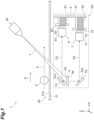
- FIG. 1 is a view showing a schematic configuration of an imaging system according to a first embodiment of the present disclosure.
- FIG. 2 is a plan view of an imaging unit shown in FIG. 1 .
- an imaging system 1 of the first embodiment is a device that acquires a radiation image of an object A.
- the imaging system 1 is an X-ray imaging system using a scintillator double-sided observation method.
- the imaging system 1 is applied to, for example, in-line X-ray inspection.
- the imaging system 1 shows good performance in discriminating, for example, a substance consisting of a light element.
- the imaging system 1 is applied to, for example, a field such as food inspection or battery inspection.
- the object A contains, for example, a substance consisting of a light element.
- a substance consisting of a light element In the field of food inspection, for example, it is inspected whether or not foreign matter is caught in food. Examples of such matter include food waste, hair, vinyl, insects, bones in meat, and the like.
- the imaging system 1 includes a conveying device 20 that conveys the object A in a predetermined conveying direction D (X-axis direction); a radiation source 30 that emits radiation L such as a white X-ray toward the object A conveyed by the conveying device 20; and an imaging unit 3A that executes image processing based on an image signal corresponding to the radiation L that has transmitted through the object A.
- a conveying device 20 that conveys the object A in a predetermined conveying direction D (X-axis direction)
- a radiation source 30 that emits radiation L such as a white X-ray toward the object A conveyed by the conveying device 20
- an imaging unit 3A that executes image processing based on an image signal corresponding to the radiation L that has transmitted through the object A.
- the conveying device 20 includes, for example, a belt conveyor 21 that moves on a revolving trajectory.
- the object A is placed or held on a conveying surface 21a of the belt conveyor 21.
- the belt conveyor 21 is a conveying stage or a conveying unit.
- the conveying device 20 includes a drive source (not shown) that drives the belt conveyor 21.
- the conveying device 20 is configured to convey the object A in the conveying direction D at a constant speed. In other words, the object A is conveyed on a predetermined conveying path P by the conveying device 20.
- the conveying direction D is a horizontal direction.
- the conveying path P has a linear shape.
- a direction in which the conveying path P extends is parallel to the conveying direction D.
- a conveying timing or a conveying speed of the object A in the conveying device 20 is set in advance and is controlled by a control unit.
- the imaging system 1 is compatible with the conveying device 20 of any form.
- the conveying direction D and the conveying path P may be horizontal.
- the conveying direction D and the conveying path P may be inclined with respect to the horizontal.
- the conveying path P may have a linear shape or a curved shape. In that case, the conveying direction D may be tangent to a portion of the conveying path P overlapping an irradiation region of the radiation.
- the conveying device 20 may not have the physical conveying surface 21a.
- the conveying device 20 may convey the object A in a state where the object A is lifted by the air.
- the conveying device 20 may convey the object A by releasing the object A to the air.
- the conveying path P may have, for example, a parabolic shape.
- the conveying device 20 may include a roller conveyor including a plurality of rollers.
- the radiation source 30 emits the radiation L.
- the radiation L is, for example, a cone beam X-ray.
- the radiation source 30 may be a microfocus X-ray source or a millifocus X-ray source.
- the radiation L emitted from the radiation source 30 forms a radiation flux.
- a presence region of the radiation flux is an emission region of the radiation source 30.
- the imaging unit 3A is disposed opposite the radiation source 30 with respect to the conveying surface 21a of the belt conveyor 21.
- the imaging unit 3A is attached to the conveying device 20 so as not to interfere with the revolving of the belt conveyor 21.
- the same also applies to the case where the conveying device 20 is a roller conveyor.
- the imaging unit 3A is disposed with some gap from the conveying unit so as not to interfere with movement of the conveying unit such as a belt conveyor, or a roller conveyor.
- the imaging unit 3A includes a scintillator 4, a first mirror 51, a second mirror 52, a first sensor module 6, a second sensor module 7, a processing substrate (image processing unit and control unit) 8, a first connection member 91, and a second connection member 92.
- the scintillator 4 is a wavelength conversion member.
- the scintillator 4 emits a scintillation light upon an incidence of the radiation L that has transmitted through the object A.
- the scintillator 4 has an oblong plate shape extending in a detection width direction (Y-axis direction).
- the scintillator 4 has a first surface 4a serving as an incident surface of the radiation L, and a second surface 4b facing the first surface 4a in a Z-axis direction.
- the first surface 4a and the second surface 4b are parallel to the conveying surface 21a of the belt conveyor 21.
- the first surface 4a faces a radiation source 30 side.
- the scintillator 4 converts the radiation L that has transmitted through the object A, into a scintillation light (visible light).
- An X-ray having a relatively low energy is converted into a scintillation light S1 by the first surface 4a of the scintillator 4, and the scintillation light S1 is output from the first surface 4a.
- an X-ray having a relatively high energy is converted into a scintillation light S2 by the second surface 4b of the scintillator 4, and the scintillation light S2 is output from the second surface 4b.
- the scintillator 4 consists of, for example, Gd 2 O 2 S:Tb, Gd 2 O 2 S:Pr, CsLTl, CdWO 4 , CaWO 4 , Gd 2 SiO 5 :Ce, Lu 0.4 Gd 1.6 SiO 5 , Bi 4 Ge 3 O 12 , Lu 2 SiO 5 :Ce, Y 2 SiO 5 , YAlO 3 :Ce, Y 2 O 2 S:Tb, YTaO 4 :Tm, YAG:Ce, YAG:Pr, YGAG:Ce, YGAG:Pr, GAGG:Ce, or the like.
- a thickness of the scintillator 4 is set to an appropriate value within a range of several ⁇ m to several mm depending on an energy band of radiation to be detected.
- the scintillator 4 may be formed of one scintillator.
- the scintillator 4 may be a combination of a plurality of scintillators. When the plurality of scintillators are combined, the types of the scintillators may be the same or different.
- the first mirror 51 is, for example, a mirror made of glass onto aluminum is evaporated or mirror-finished metal.
- the first mirror 51 is disposed on the radiation source 30 side with respect to the scintillator 4.
- the first mirror 51 has an oblong plate shape extending in the detection width direction (Y-axis direction).
- the first mirror 51 has a reflective surface 51a.
- the reflective surface 51a forms at an acute angle with respect to the first surface 4a of the scintillator 4.
- the reflective surface 51a obliquely faces the first surface 4a, and obliquely faces the first sensor module 6.
- the reflective surface 51a reflects the scintillation light S1 emitted from the first surface 4a, toward the first sensor module 6.
- the second mirror 52 is, for example, a mirror made of glass onto aluminum is evaporated or mirror-finished metal.
- the second mirror 52 is disposed opposite the first mirror 51 with respect to the scintillator 4.
- the second mirror 52 has an oblong plate shape extending in the detection width direction (Y-axis direction).
- the second mirror 52 has a reflective surface 52a.
- the reflective surface 52a forms at an acute angle with respect to the second surface 4b of the scintillator 4.
- the reflective surface 52a obliquely faces the second surface 4b, and obliquely faces the second sensor module 7.
- the reflective surface 52a reflects the scintillation light S2 emitted from the second surface 4b, toward the second sensor module 7.
- the reflective surface 51a has an area sufficient enough to reflect the scintillation light S1 emitted in a normal direction of the first surface 4a.
- the reflective surface 52a has an area sufficient enough to reflect the scintillation light S2 emitted in a normal direction of the second surface 4b. It is preferable that each of an angle between the reflective surface 51a and the first surface 4a and an angle between the reflective surface 52a and the second surface 4b is an angle within a range of 40 degrees or more 50 degrees or less. In the present embodiment, the angle is 45 degrees. The angle may be determined based on the disposition of the radiation source 30 or the position of a slit of a housing to be described later. Depending on the magnitude of the angle, the disposition of the first sensor module 6 and the second sensor module 7 may be appropriately adjusted.
- the first sensor module 6 is disposed apart from the scintillator 4 on one side (downstream side of the scintillator 4 in the conveying direction D) of the X-axis direction (in-plane direction of the first surface 4a and the second surface 4b of the scintillator 4).
- the first sensor module 6 is disposed on a first surface 4a side of the scintillator 4 in the Z-axis direction (facing direction between the first surface 4a and the second surface 4b of the scintillator 4).
- the first sensor module 6 detects the scintillation light S1 emitted from the first surface 4a upon an incidence of the radiation L, as a first scintillation light.
- the first scintillation light refers to a scintillation light detected by the first sensor module.
- the first sensor module 6 captures an image of the object A according to movement of the object A.
- the first sensor module 6 is a lens-coupled detector.
- the first sensor module 6 includes a first lens 61, a first body 62, and a first sensor 63.
- the first lens 61 is attached to the first body 62.
- the first lens 61 faces the reflective surface 51a of the first mirror 51 in the X-axis direction.
- An optical axis of the first lens 61 is parallel to the X-axis direction.
- the first lens 61 is focused on the reflective surface 51a.
- a visual field 61a of the first lens 61 extends over a wide range of the reflective surface 51a in the Y-axis direction.
- the first lens 61 condenses the scintillation light S1 reflected by the reflective surface 51a.
- the first sensor 63 is provided inside the first body 62. The first sensor 63 detects the scintillation light S1 condensed by the first lens 61, and outputs a first image signal corresponding to a detection result.
- the first sensor 63 is an image sensor.
- the first sensor 63 is, for example, a general line sensor, a multi-line sensor, or an area image sensor that can be driven in a time delay integration (TDI) mode.
- the first sensor 63 is, for example, a CCD area image sensor or a CMOS image sensor.
- the first sensor 63 has an element row along which a plurality of light-receiving elements are arranged in a row in a pixel direction.
- the image pitches of the plurality of light-receiving elements may be the same or different.
- a plurality of stages of the element rows are arranged in an integration direction to correspond to a movement direction of the object A.
- the first sensor 63 has a scanning direction corresponding to the conveying direction D of the object A, and a line direction orthogonal to the scanning direction.
- the scanning direction is the foregoing integration direction, and is parallel to the Z-axis direction.
- the line direction is the foregoing pixel direction, and is parallel to the Y-axis direction.
- the scanning direction is a direction that is converted from the conveying direction D via the first mirror 51. In the present embodiment, the scanning direction is converted from the conveying direction D by 90 degrees.
- the first sensor 63 is controlled by the control unit to perform charge transfer according to movement of the object A. Namely, the first sensor 63 performs charge transfer on a light receiving surface in synchronization with movement of the object A by the conveying device 20. Accordingly, a radiation image having a good S/N ratio can be obtained
- the control unit is configured to control the radiation source 30 and the first sensor module 6 to turn on the radiation source 30 according to an imaging timing of the first sensor module 6.
- the first sensor module 6 may be controlled by a signal from an encoder provided on a stage.
- the second sensor module 7 is disposed apart from the scintillator 4 on the one side in the X-axis direction.
- the second sensor module 7 is disposed on a second surface 4b side of the scintillator 4 in the Z-axis direction.
- the second sensor module 7 detects the scintillation light S2 emitted from the second surface 4b upon an incidence of the radiation L, as a second scintillation light.
- the second scintillation light refers to a scintillation light detected by the second sensor module.
- the second sensor module 7 captures an image of the object A according to movement of the object A.
- the second sensor module 7 is a lens-coupled detector.
- the second sensor module 7 includes a second lens 71, a second body 72, and a second sensor 73.
- the second lens 71 is attached to the second body 72.
- the second lens 71 faces the reflective surface 52a of the second mirror 52 in the X-axis direction.
- An optical axis of the second lens 71 is parallel to the X-axis direction.
- the second lens 71 is focused on the reflective surface 52a.
- a visual field 71a of the second lens 71 extends over a wide range of the reflective surface 52a in the Y-axis direction.
- the second lens 71 condenses the scintillation light S2 reflected by the reflective surface 52a.
- the second sensor 73 is provided inside the second body 72.
- the second sensor 73 detects the scintillation light S2 condensed by the second lens 71, and outputs a second image signal corresponding to a detection result.
- the second sensor 73 has the same configuration as that of the first sensor 63, and is controlled in the same manner as in the first sensor 63. A detailed description of the second sensor 73 will not be repeated.
- the processing substrate 8 includes a substrate 81 and a processor (not shown) attached to the substrate 81.
- the processing substrate 8 functions as an image processing unit that executes image processing based on the first image signal output from the first sensor 63 and on the second image signal output from the second sensor 73. Specifically, the processing substrate 8 performs image processing such as magnification correction, luminance value correction, dark correction, shading correction, affine transformation processing, edge enhancement processing, noise removal processing, bilateral filtering, or view angle adjustment on at least one of the first image signal and the second image signal.
- the processing substrate 8 outputs a radiation image created by executing the image processing, to a computer.
- the processing substrate 8 functions as a control unit that controls imaging conditions of the first sensor 63 and imaging conditions of the second sensor 73. Specifically, the processing substrate 8 sets an exposure time, a gain, an imaging frequency, an imaging timing, and the like for the first sensor 63 and the second sensor 73. In addition, the processing substrate 8 adjusts the imaging timing of the first sensor 63, the imaging timing of the second sensor 73, and image processing timing as the image processing unit and as the control unit. Accordingly, a process of causing the detection ranges of the first image signal and the second image signal to coincide with each other and a process of such as comparing or combining the first image signal and the second image signal are facilitated. The processing substrate 8 may perform control to delay the output of at least one of the first image signal and the second image signal within a range more than the exposure time.
- one processing substrate 8 is provided for the first sensor module 6 and the second sensor module 7. Namely, the processing substrate 8 is common to the first sensor module 6 and the second sensor module 7.
- the first connection member 91 electrically connects the first sensor module 6 and the processing substrate 8. Specifically, the first connection member 91 electrically connects the first sensor 63 and the image processing processor via wirings provided on the first body 62 and via wirings provided on the substrate 81.
- the second connection member 92 electrically connects the second sensor module 7 and the processing substrate 8. Specifically, the second connection member 92 electrically connects the second sensor 73 and the image processing processor via wirings provided on the second body 72 and via wirings provided on the substrate 81. Accordingly, the first image signal and the second image signal can be output to the processing substrate 8.
- Each of the first connection member 91 and the second connection member 92 has flexibility. Each of the first connection member 91 and the second connection member 92 is easily deformable to the extent that the first connection member 91 and the second connection member 92 receive a load corresponding to, for example, a force of worker's fingers.
- Each of the first connection member 91 and the second connection member 92 is formed of, for example, a cable, a connector, and the like.
- Each of the first connection member 91 and the second connection member 92 is formed of, for example, a harness, a connector, and the like.
- Each of the first connection member 91 and the second connection member 92 is, for example, a flexible connector.
- the imaging unit 3A includes, for example, a housing (not shown) having a rectangular parallelepiped shape.
- the scintillator 4, the first mirror 51, the second mirror 52, the first sensor module 6, the second sensor module 7, and the processing substrate 8 are housed in the housing.
- Each of the scintillator 4, the first mirror 51, the second mirror 52, the first sensor module 6, the second sensor module 7, and the processing substrate 8 is held by the housing.
- a slit through which the radiation L emitted from the radiation source 30 passes is formed in a wall portion on the radiation source 30 side of the housing.
- the slit has, for example, an oblong shape extending in the detection width direction (Y-axis direction).
- the housing is made of, for example, a material capable of blocking X-rays.
- the housing is a so-called dark box.
- the housing may be made of, for example, metal.
- the housing is made of, for example, aluminum, iron, stainless steel, or the like.
- the housing may contain a protective material.
- the protective material is, for example, metal. Examples of the protective material include lead, tungsten, copper, iron, stainless steel, and the like.
- the housing has a shape that is long in the conveying direction D. The housing may be attached to the conveying device 20.
- the imaging system 1 includes the control unit (not shown).
- the control unit controls the radiation source 30 based on a value of a tube voltage or a tube current of the radiation source 30 stored by a user's input or the like.
- the control unit controls each of the first sensor module 6 and the second sensor module 7 based on the exposure time and the like of each of the first sensor module 6 and the second sensor module 7 stored by a user's input or the like.
- the control unit and the image processing processor of the processing substrate 8 may be separate processors or the same processor.
- An interval between the reflective surface 51a and the first surface 4a of the scintillator 4 in the Z-axis direction is smaller than an interval between the reflective surface 52a and the second surface 4b of the scintillator 4 in the Z-axis direction.
- an optical path length of the scintillation light S1 in the Z-axis direction between the reflective surface 51a and the first surface 4a is smaller than an optical path length of the scintillation light S2 in the Z-axis direction between the reflective surface 52a and the second surface 4b.
- An interval between the first lens 61 and the first surface 4a of the scintillator 4 in the Z-axis direction is smaller than an interval between the second lens 71 and the second surface 4b of the scintillator 4 in the Z-axis direction.
- an interval between the optical axis of the first lens 61 and the first surface 4a is smaller than an interval between the optical axis of the second lens 71 and the second surface 4b.
- a position of the second lens 71 in the X-axis direction is closer to a scintillator 4 side than a position of the first lens 61 in the X-axis direction.
- an optical path length of the scintillation light S2 in the X-axis direction between the reflective surface 52a and the second lens 71 is smaller than an optical path length of the scintillation light S1 in the X-axis direction between the reflective surface 51a and the first lens 61.
- An optical path length of the scintillation light S1 between the first surface 4a of the scintillator 4 and the first lens 61 is equal to an optical path length of the scintillation light S2 between the second surface 4b of the scintillator 4 and the second lens 71.
- the sum of the optical path length of the scintillation light S1 in the Z-axis direction between the reflective surface 51a and the first surface 4a and the optical path length of the scintillation light S1 in the X-axis direction between the reflective surface 51a and the first lens 61 is equal to the sum of the optical path length of the scintillation light S2 in the Z-axis direction between the reflective surface 52a and the second surface 4b and the optical path length of the scintillation light S2 in the X-axis direction between the reflective surface 52a and the second lens 71.
- the first mirror 51 and the first sensor module 6 are disposed close to the scintillator 4 in the Z-axis direction, and the optical path length of the scintillation light S1 and the scintillation light S2 are set to coincide with each other. Accordingly, the scintillator 4 can be disposed close to the object A, and a radiation image of the object A can be accurately acquired.
- each of the first connection member 91 and the second connection member 92 has flexibility. Namely, the first sensor module 6 and the second sensor module 7 are connected to the processing substrate 8 by the first connection member 91 and the second connection member 92, and the positions thereof with respect to the processing substrate 8 can be adjusted. Accordingly, the above-described positional relationship can be easily adjusted by adjusting the position of each of the first sensor module 6 and the second sensor module 7.
- the object A is conveyed in the conveying direction D by the conveying device 20.
- the radiation source 30 emits the radiation L toward the object A.
- the radiation L that has transmitted through the object A is incident on the first surface 4a.
- the radiation L is converted into a scintillation light by the scintillator 4.
- the scintillation light S1 emitted from the first surface 4a is reflected by the first mirror 51, and is imaged on the first sensor 63 by the first lens 61 of the first sensor module 6.
- the first sensor 63 captures an image of the scintillation light S1 (scintillation image) imaged by the first lens 61.
- the first sensor module 6 outputs the radiation image data (first image signal) obtained by imaging, to the processing substrate 8.
- the second sensor module 7 captures an image of the scintillation light S2, and outputs the obtained radiation image data (second image signal) to the processing substrate 8.
- the radiation image data is input to the processing substrate 8, and the processing substrate 8 executes predetermined processing such as image processing on the input radiation image data to create a radiation image.
- the processing substrate 8 outputs the created radiation image to the computer.
- the computer displays the radiation image output from the processing substrate 8. As described above, the radiation image is obtained by double-sided observation of the object A.
- the processing substrate 8 that processes the first image signal and the second image signal from the first sensor module 6 and the second sensor module 7 is common. Therefore, the configuration is simplified compared to a configuration in which a processing substrate is provided for each sensor module.
- each of the first connection member 91 and the second connection member 92 that connect the first sensor module 6 and the second sensor module 7 to the processing substrate 8, respectively has flexibility for common use of the processing substrate 8. For this reason, the imaging positions of the first sensor module 6 and the second sensor module 7 can be separately adjusted, and the degree of freedom in adjusting the imaging positions can be sufficiently ensured.
- the imaging unit 3A includes the scintillator 4 that emits the scintillation lights S1 and S2 upon an incidence of the radiation L. Accordingly, workability when the imaging unit 3A is assembled to the imaging system 1 can be improved.
- the scintillator 4 has the first surface 4a serving as an incident surface of the radiation L, and the second surface 4b facing the first surface 4a.
- the first sensor module 6 is disposed on the first surface 4a side of the scintillator 4 in the Z-axis direction.
- the first sensor module 6 detects the scintillation light S1 emitted from the first surface 4a upon an incidence of the radiation L, as the first scintillation light.
- the second sensor module 7 is disposed on the second surface 4b side of the scintillator 4 in the Z-axis direction.
- the second sensor module 7 detects the scintillation light S2 emitted from the second surface 4b upon an incidence of the radiation L, as the second scintillation light. Accordingly, for example, dual-energy imaging using a scintillation light in a low energy band and a scintillation light in a high energy band can be suitably realized.
- the first sensor module 6 and the second sensor module 7 are disposed apart from the scintillator 4 on the one side in the X-axis direction.
- the interval between the first lens 61 of the first sensor module 6 and the first surface 4a in the Z-axis direction is smaller than the interval between the second lens 71 of the second sensor module 7 and the second surface 4b in the Z-axis direction.
- the position of the second lens 71 in the X-axis direction is closer to the scintillator 4 side than the position of the first lens 61 in the Z-axis direction. Accordingly, when the imaging unit 3A is assembled to the imaging system 1, the first surface 4a of the scintillator 4 can be disposed close to the object A.
- the optical path length of the scintillation light S1 (first scintillation light) and the optical path length of the scintillation light S2 (second scintillation light) can be set to coincide with each other.
- the configuration can be simplified, and the degree of freedom in adjusting the imaging positions can be sufficiently ensured.
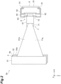
- FIG. 3 is a view showing a schematic configuration of an imaging unit according to a second embodiment of the present disclosure.
- FIG. 4 is a plan view of the imaging unit shown in FIG. 3 .
- an imaging unit 3B according to the second embodiment differs from the imaging unit 3A of the first embodiment in that the first sensor module 6 and the second sensor module 7 are disposed on the first surface 4a side of the scintillator 4 and are arranged in the Y-axis direction and the second mirror 52 is not provided.
- An imaging system is an X-ray imaging system using a scintillator front surface observation method.
- the first sensor module 6 and the second sensor module 7 are disposed on the first surface 4a side of the scintillator 4 in the Z-axis direction, and are arranged in the Y-axis direction (in-plane direction of the first surface 4a).
- the first sensor module 6 detects the scintillation light S1 emitted from the first surface 4a upon an incidence of the radiation L, as a first scintillation light.
- the second sensor module 7 detects the scintillation light S1 emitted from the first surface 4a upon an incidence of the radiation L, as a second scintillation light.
- An interval between the first lens 61 of the first sensor module 6 and the scintillator 4 in the Z-axis direction is equal to an interval between the second lens 71 of the second sensor module 7 and the scintillator 4 in the Z-axis direction.
- an interval between the optical axis of the first lens 61 and the first surface 4a is equal to an interval between the optical axis of the second lens 71 and the first surface 4a.
- an optical path length of the scintillation light S1 (the scintillation light S1 to be incident on the first lens 61) in the Z-axis direction between the reflective surface 51a of the first mirror 51 and the first surface 4a is equal to an optical path length of the scintillation light S1 (the scintillation light S1 to be incident on the second lens 71) in the Z-axis direction between the reflective surface 51a and the first surface 4a.
- an optical path length of the scintillation light S1 in the X-axis direction between the reflective surface 51a and the first lens 61 is equal to an optical path length of the scintillation light S1 in the X-axis direction between the reflective surface 51a and the second lens 71.
- an optical path length of the scintillation light S1 between the first surface 4a of the scintillator 4 and the first lens 61 is equal to an optical path length of the scintillation light S1 between the first surface 4a of the scintillator 4 and the second lens 71.
- FIG. 5 is a view showing visual fields of the first lens 61 and the second lens 71 shown in FIG. 3 .
- the first mirror 51 is not shown.
- the visual fields of the first lens 61 and the second lens 71 partially overlap each other in the Y-axis direction.
- the range of the visual field 61a of the first lens 61 in the Y-axis direction with respect to the first surface 4a and the range of the visual field 61a of the second lens 71 in the Y-axis direction with respect to the first surface 4a partially overlap each other.
- the range of the visual field 61a of the first lens 61 in the Y-axis direction and the range of the visual field 71a of the second lens 71 in the Y-axis direction partially overlap each other on the reflective surface 51a (refer to FIG. 3 ) of the first mirror 51.
- An overlapping region R exists between the visual field 61a and the visual field 71a.
- a width of the overlapping region R in the Y-axis direction can be adjusted by adjusting the positions of the first sensor module 6 and the second sensor module 7 in the Y-axis direction.
- the first sensor module 6 and the second sensor module 7 are arranged in the Y-axis direction, so that a visual field of the imaging unit 3B in the Y-axis direction is widened, and the overlapping region R is appropriately provided, so that the visual field 61a and the visual field 71a are continuous with each other in the Y-axis direction.
- the first connection member 91 and the second connection member 92 have flexibility, the position of each of the first sensor module 6 and the second sensor module 7 with respect to the processing substrate 8 can be adjusted. Accordingly, the above-described positional relationship can be easily adjusted by adjusting the position of each of the first sensor module 6 and the second sensor module 7.
- the scintillator 4 has the first surface 4a serving as an incident surface of the radiation L, and the second surface 4b facing the first surface 4a.
- the first sensor module 6 and the second sensor module 7 are disposed on the first surface 4a side of the scintillator 4 in the Z-axis direction, and are arranged in the Y-axis direction.
- the first sensor module 6 detects the scintillation light S1 emitted from the first surface 4a upon an incidence of the radiation L, as the first scintillation light.
- the second sensor module 7 detects the scintillation light S1 emitted from the first surface 4a upon an incidence of the radiation L, as the second scintillation light. Accordingly, the respective scintillation lights S1 from single side of the scintillator 4 can be accurately detected by the first sensor module 6 and the second sensor module 7.
- the visual field 61a of the first lens 61 of the first sensor module 6 and the visual field 71a of the second lens 71 of the second sensor module 7 partially overlap each other in the Z-axis direction. Accordingly, the visual field 61a of the first lens 61 and the visual field 71a of the second lens 71 are continuous with each other, and an image of the scintillation light S1 can be captured over a wide range without a blind spot.
- the first sensor module 6 and the second sensor module 7 are disposed apart from the scintillator 4 on the one side in the X-axis direction.
- the interval between the first lens 61 of the first sensor module 6 and the scintillator 4 in the Z-axis direction is equal to the interval between the second lens 71 of the second sensor module 7 and the scintillator 4 in the Z-axis direction.
- the positions of the first lens 61 and the second lens 71 in the X-axis direction with respect to the scintillator 4 coincide with each other. Accordingly, the first lens 61 and the second lens 71 can be common.
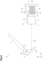
- FIG. 6 is a view showing a schematic configuration of an imaging unit according to a third embodiment of the present disclosure.
- FIG. 7 is a plan view of the imaging unit shown in FIG. 6 .
- an imaging unit 3C according to the third embodiment differs from the imaging unit 3B of the second embodiment in that the first sensor module 6 and the second sensor module 7 are disposed on the second surface 4b side of the scintillator 4, and in that the first mirror 51 is not provided and the second mirror 52 is provided.
- An imaging system is an X-ray imaging system using a scintillator back surface observation method.
- the first sensor module 6 and the second sensor module 7 are disposed on the second surface 4b side of the scintillator 4 in the Z-axis direction.
- the first sensor module 6 detects the scintillation light S2 emitted from the second surface 4b upon an incidence of the radiation L, as a first scintillation light.
- the second sensor module 7 detects the scintillation light S2 emitted from the second surface 4b upon an incidence of the radiation L, as a second scintillation light.
- an interval between the optical axis of the first lens 61 and the second surface 4b is equal to an interval between the optical axis of the second lens 71 and the second surface 4b, and the positions of the first lens 61 and the second lens 71 in the X-axis direction with respect to the scintillator 4 coincide with each other.
- the visual fields of the first lens 61 and the second lens 71 partially overlap each other in the Y-axis direction.
- the scintillator 4 has the first surface 4a serving as an incident surface of the radiation L, and the second surface 4b facing the first surface 4a.
- the first sensor module 6 and the second sensor module 7 are disposed on the second surface 4b side of the scintillator 4 in the Z-axis direction, and are arranged in the Y-axis direction.
- the first sensor module 6 detects the scintillation light S2 emitted from the second surface 4b upon an incidence of the radiation L, as the first scintillation light.
- the second sensor module 7 detects the scintillation light S2 emitted from the second surface 4b upon an incidence of the radiation L, as the second scintillation light. Accordingly, the respective scintillation lights S2 from single side of the scintillator 4 can be accurately detected by the first sensor module 6 and the second sensor module 7.
- the imaging units 3A, 3B, and 3C include the scintillator 4, but the imaging units 3A, 3B, and 3C may not include the scintillator 4.
- the scintillator 4 may not be a configuration of the imaging units 3A, 3B, and 3C.
- the scintillator 4 may be a configuration of the imaging system.
- imaging system 3A, 3B, 3C: imaging unit
- 4 scintillator
- 4a first surface
- 4b second surface
- 6 first sensor module
- 7 second sensor module
- 8 processing substrate
- 20 conveying device
- 30 radiation source
- 61 first lens
- 61a visual field
- 63 first sensor
- 71 second lens
- 73 second sensor
- 91 first connection member
- 92 second connection member
- A object
- L radiation
- S1, S2 scintillation light.
Landscapes
- Physics & Mathematics (AREA)
- General Physics & Mathematics (AREA)
- Health & Medical Sciences (AREA)
- Life Sciences & Earth Sciences (AREA)
- High Energy & Nuclear Physics (AREA)
- Molecular Biology (AREA)
- Spectroscopy & Molecular Physics (AREA)
- Chemical & Material Sciences (AREA)
- Analytical Chemistry (AREA)
- Biochemistry (AREA)
- General Health & Medical Sciences (AREA)
- Immunology (AREA)
- Pathology (AREA)
- Crystallography & Structural Chemistry (AREA)
- Engineering & Computer Science (AREA)
- Theoretical Computer Science (AREA)
- Measurement Of Radiation (AREA)
- Lens Barrels (AREA)
- Studio Devices (AREA)
Applications Claiming Priority (2)
| Application Number | Priority Date | Filing Date | Title |
|---|---|---|---|
| JP2020195049 | 2020-11-25 | ||
| PCT/JP2021/035165 WO2022113507A1 (ja) | 2020-11-25 | 2021-09-24 | 撮像ユニット及び撮像システム |
Publications (2)
| Publication Number | Publication Date |
|---|---|
| EP4206745A1 true EP4206745A1 (de) | 2023-07-05 |
| EP4206745A4 EP4206745A4 (de) | 2024-08-14 |
Family
ID=81755522
Family Applications (1)
| Application Number | Title | Priority Date | Filing Date |
|---|---|---|---|
| EP21897485.5A Pending EP4206745A4 (de) | 2020-11-25 | 2021-09-24 | Bildgebungseinheit und bildgebungssystem |
Country Status (7)
| Country | Link |
|---|---|
| US (1) | US20230400421A1 (de) |
| EP (1) | EP4206745A4 (de) |
| JP (1) | JP7724238B2 (de) |
| KR (1) | KR20230109134A (de) |
| CN (1) | CN116472474A (de) |
| TW (1) | TW202223372A (de) |
| WO (1) | WO2022113507A1 (de) |
Families Citing this family (1)
| Publication number | Priority date | Publication date | Assignee | Title |
|---|---|---|---|---|
| EP4579286A4 (de) * | 2022-08-23 | 2026-01-21 | Toray Industries | Röntgenuntersuchungsvorrichtung und röntgenuntersuchungsverfahren |
Family Cites Families (111)
| Publication number | Priority date | Publication date | Assignee | Title |
|---|---|---|---|---|
| US4338521A (en) * | 1980-05-09 | 1982-07-06 | General Electric Company | Modular radiation detector array and module |
| US4578803A (en) * | 1981-12-07 | 1986-03-25 | Albert Macovski | Energy-selective x-ray recording and readout system |
| US5040199A (en) * | 1986-07-14 | 1991-08-13 | Hologic, Inc. | Apparatus and method for analysis using x-rays |
| US5864146A (en) * | 1996-11-13 | 1999-01-26 | University Of Massachusetts Medical Center | System for quantitative radiographic imaging |
| EP1116047B1 (de) * | 1998-09-24 | 2006-07-12 | Elgems Ltd. | Photonendetektor in form einer pixel-matrix |
| WO2000025149A1 (en) * | 1998-10-28 | 2000-05-04 | Koninklijke Philips Electronics N.V. | Computer tomograph detector |
| US6019610A (en) * | 1998-11-23 | 2000-02-01 | Glatts, Iii; George F. | Elastomeric connector |
| US6353657B1 (en) * | 1998-11-27 | 2002-03-05 | Wuestec Medical, Inc. | Image redirection and optical path folding |
| US6396898B1 (en) * | 1999-12-24 | 2002-05-28 | Kabushiki Kaisha Toshiba | Radiation detector and x-ray CT apparatus |
| JP2002034961A (ja) | 2000-07-31 | 2002-02-05 | Konica Corp | 放射線撮影装置及び放射線撮影方法 |
| US6658082B2 (en) * | 2000-08-14 | 2003-12-02 | Kabushiki Kaisha Toshiba | Radiation detector, radiation detecting system and X-ray CT apparatus |
| US6671345B2 (en) * | 2000-11-14 | 2003-12-30 | Koninklijke Philips Electronics N.V. | Data acquisition for computed tomography |
| JP4476471B2 (ja) * | 2000-11-27 | 2010-06-09 | 株式会社東芝 | X線コンピュータ断層撮影装置 |
| US6473486B2 (en) * | 2000-12-05 | 2002-10-29 | Ge Medical Systems Global Technology Co., Llc | System and method of computed tomography imaging using a focused scintillator and method of manufacturing |
| US6873678B2 (en) * | 2000-12-28 | 2005-03-29 | Ge Medical Systems Global Technology Company Llc | Methods and apparatus for computed tomographic cardiac or organ imaging |
| US6522715B2 (en) * | 2000-12-29 | 2003-02-18 | Ge Medical Systems Global Technology Company Llc | High density flex interconnect for CT detectors |
| DE10116222A1 (de) * | 2001-03-30 | 2002-10-17 | Siemens Ag | Detektor für Röntgen-Computertomograph |
| JP2003084066A (ja) * | 2001-04-11 | 2003-03-19 | Nippon Kessho Kogaku Kk | 放射線検出器用部品、放射線検出器および放射線検出装置 |
| JP2002365368A (ja) * | 2001-06-04 | 2002-12-18 | Anritsu Corp | X線検出器及び該検出器を用いたx線異物検出装置 |
| US6510195B1 (en) * | 2001-07-18 | 2003-01-21 | Koninklijke Philips Electronics, N.V. | Solid state x-radiation detector modules and mosaics thereof, and an imaging method and apparatus employing the same |
| JP2003130961A (ja) * | 2001-07-19 | 2003-05-08 | Siemens Ag | 検出器モジュール、x線コンピュータトモグラフ用の検出器およびx線コンピュータトモグラフによる断層像の作成方法 |
| US6982423B2 (en) * | 2001-11-20 | 2006-01-03 | Koninklijke Philips Electronics N.V. | CT detector-module having radiation shielding for the processing circuitry |
| US7171031B2 (en) * | 2002-04-30 | 2007-01-30 | Fuji Photo Film Co., Ltd. | Method, apparatus, and program for restoring phase information |
| US6917664B2 (en) * | 2002-10-03 | 2005-07-12 | Koninklijke Philips Electronics N.V. | Symmetrical multiple-slice computed tomography data management system |
| US7103140B2 (en) * | 2002-11-26 | 2006-09-05 | Konica Minolta Medical & Graphic Inc. | Radiation image radiographic apparatus |
| US7492857B2 (en) * | 2002-12-19 | 2009-02-17 | General Electric Company | Self-aligning scintillator-collimator assembly |
| US7190759B2 (en) * | 2002-12-19 | 2007-03-13 | General Electric Company | Support structure for Z-extensible CT detectors and methods of making same |
| JP2004208773A (ja) * | 2002-12-27 | 2004-07-29 | Konica Minolta Holdings Inc | 放射線画像形成システム |
| JP4833554B2 (ja) * | 2003-01-06 | 2011-12-07 | コーニンクレッカ フィリップス エレクトロニクス エヌ ヴィ | 放射線検出器モジュールと該放射線検出器モジュールを用いたコンピュータ断層撮影用スキャナ、および放射線検出方法 |
| DE10301941B4 (de) * | 2003-01-20 | 2005-11-17 | Fraunhofer-Gesellschaft zur Förderung der angewandten Forschung e.V. | Kamera und Verfahren zur optischen Aufnahme eines Schirms |
| DE10332333B4 (de) * | 2003-07-16 | 2006-08-03 | Siemens Ag | Detektormodul |
| JP2006528017A (ja) * | 2003-07-22 | 2006-12-14 | コーニンクレッカ フィリップス エレクトロニクス エヌ ヴィ | 2次元ct検出器用放射線マスク |
| US7010092B2 (en) * | 2003-08-08 | 2006-03-07 | Imaging Dynamics Company Ltd. | Dual energy imaging using optically coupled digital radiography system |
| US7019304B2 (en) * | 2003-10-06 | 2006-03-28 | General Electric Company | Solid-state radiation imager with back-side irradiation |
| EP1695117A1 (de) * | 2003-12-09 | 2006-08-30 | Philips Intellectual Property & Standards GmbH | Abschirmung für einen röntgendetektor |
| DE102004001688B4 (de) * | 2004-01-12 | 2010-01-07 | Siemens Ag | Detektormodul |
| US7525097B2 (en) * | 2004-04-06 | 2009-04-28 | Koninklijke Philips Electronics N.V. | Modular device for the detection and/or transmission of radiation with self-aligning modules |
| US7286640B2 (en) * | 2004-04-09 | 2007-10-23 | Xradia, Inc. | Dual-band detector system for x-ray imaging of biological samples |
| US7412024B1 (en) * | 2004-04-09 | 2008-08-12 | Xradia, Inc. | X-ray mammography |
| US7439516B2 (en) * | 2004-10-01 | 2008-10-21 | General Electric Company | Module assembly for multiple die back-illuminated diode |
| DE102004049917A1 (de) * | 2004-10-13 | 2006-04-20 | Siemens Ag | Röntgendetektoreinrichtung und Verfahren zum Herstellen einer Röntgendetektoreinrichtung |
| DE102004057533B4 (de) * | 2004-11-29 | 2007-12-27 | Siemens Ag | Detektor mit mehreren Detektorriegeln und Computertomographiegerät mit einem solchen Detektor |
| DE102005007485B4 (de) * | 2005-02-17 | 2008-05-08 | Siemens Ag | Zwischenstecker für einen Detektor und Verfahren zur Durchführung einer Fehlersuche bei einem Detektor mit einem solchen Zwischenstecker |
| DE102005014187B4 (de) * | 2005-03-29 | 2017-02-23 | Siemens Healthcare Gmbh | Detektormodul, Detektor und Computertomographiegerät |
| JP4764050B2 (ja) * | 2005-03-31 | 2011-08-31 | 株式会社日立製作所 | 核医学診断装置および核医学診断装置の冷却方法 |
| JP3942188B2 (ja) * | 2005-09-30 | 2007-07-11 | 株式会社日立製作所 | 核医学診断装置、陽電子放出型断層撮影装置及び検出器ユニット |
| CN101278208A (zh) * | 2005-10-05 | 2008-10-01 | 皇家飞利浦电子股份有限公司 | 使用薄电路的计算机断层摄影探测器 |
| US7560702B2 (en) * | 2005-11-28 | 2009-07-14 | General Electric Company | Interconnect and packaging method for multi-slice CT detector modules |
| US7582879B2 (en) * | 2006-03-27 | 2009-09-01 | Analogic Corporation | Modular x-ray measurement system |
| RU2408110C2 (ru) * | 2006-03-30 | 2010-12-27 | Конинклейке Филипс Электроникс, Н.В. | Матрица детекторов излучения |
| US7405406B1 (en) * | 2006-04-21 | 2008-07-29 | Radiation Monitoring Devices, Inc. | Two-sided scintillation detectors and related methods |
| EP1857836B1 (de) * | 2006-05-15 | 2009-10-21 | Eldim Sa | Vorrichtung und Methode zur Unterscheidung von Cerenkovstrahlung und Szintillationsstrahlung |
| US7504637B2 (en) * | 2006-07-11 | 2009-03-17 | Aeroflex Colorado Springs Inc. | Two component photodiode detector |
| US7429737B2 (en) * | 2006-11-09 | 2008-09-30 | Carestream Health, Inc. | Retrofit digital mammography detector |
| JP5091505B2 (ja) * | 2007-02-28 | 2012-12-05 | 株式会社東芝 | 放射線検出器及びx線ct装置 |
| CN101765790B (zh) * | 2007-07-25 | 2013-02-13 | 皇家飞利浦电子股份有限公司 | Mr/pet成像系统 |
| JP2009085642A (ja) * | 2007-09-28 | 2009-04-23 | Fujifilm Corp | 放射線画像撮影装置 |
| US7812314B1 (en) * | 2007-11-06 | 2010-10-12 | The United Sttes of America as represented by the United States Department of Energy | Flat panel X-ray detector with reduced internal scattering for improved attenuation accuracy and dynamic range |
| JP5032276B2 (ja) * | 2007-11-19 | 2012-09-26 | 株式会社東芝 | 放射線検出装置 |
| DE102008064633B4 (de) * | 2008-02-06 | 2017-05-04 | Fraunhofer-Gesellschaft zur Förderung der angewandten Forschung e.V. | Vorrichtung und Verfahren zum Erfassen eines Bildes |
| US7807975B2 (en) * | 2008-02-06 | 2010-10-05 | Fraunhofer-Gesellschaft Zur Foerderung Der Angewandten Forschung E.V. | Apparatus and method for detecting an image |
| KR101269782B1 (ko) * | 2008-10-03 | 2013-05-30 | 도시바 덴시칸 디바이스 가부시키가이샤 | 방사선 검출 장치와 방사선 촬영 장치 |
| JP5559471B2 (ja) * | 2008-11-11 | 2014-07-23 | 浜松ホトニクス株式会社 | 放射線検出装置、放射線画像取得システム、放射線検査システム、及び放射線検出方法 |
| ES2346623B1 (es) | 2009-01-07 | 2011-10-03 | Consejo Superior De Investigaciones Científicas (Csic) | Sistema compacto, hibrido e integrado gamma/rf para la formacion de imagenes simultaneas petspect/mr. |
| JP5503883B2 (ja) * | 2009-03-06 | 2014-05-28 | 株式会社東芝 | X線ct装置及びx線検出装置 |
| US8098794B1 (en) * | 2009-09-11 | 2012-01-17 | The United States Of America As Represented By The Administrator Of The National Aeronautics And Space Administration | Moving-article X-ray imaging system and method for 3-D image generation |
| BR112012014166A2 (pt) * | 2009-12-15 | 2016-05-17 | Koninkl Philips Electronics Nv | recorte de imagem do detector de um sistema de geração de imagens e método |
| WO2011089528A2 (en) * | 2010-01-22 | 2011-07-28 | DenCT Ltd | Methods and apparatus for multi-camera x-ray flat panel detector |
| DE102010011582B4 (de) * | 2010-03-16 | 2011-12-01 | Siemens Aktiengesellschaft | Detektormodul für einen Strahlendetektor und Strahlendetektor |
| DE102010016502A1 (de) * | 2010-04-19 | 2011-10-20 | Phoenix Conveyor Belt Systems Gmbh | Einrichtung zur zerstörungsfreien Inspektion eines Fördergurtes mittels energiereicher Strahlen, insbesondere Röntgenstrahlen |
| US8670522B2 (en) * | 2010-07-16 | 2014-03-11 | Korea Atomic Energy Research Institute | Stereo X-ray inspection apparatus and method for forming three-dimensional image through volume reconstruction of image acquired from the same |
| DE102010062133B4 (de) * | 2010-11-29 | 2017-02-23 | Siemens Healthcare Gmbh | Kollimator für einen Strahlendetektor und Verfahren zur Herstellung eines solchen Kollimators sowie Verfahren zur Herstellung eines Kollimatoren aufweisenden Strahlendetektors |
| DE102010062192B3 (de) * | 2010-11-30 | 2012-06-06 | Siemens Aktiengesellschaft | 2D-Kollimator für einen Strahlendetektor und Verfahren zur Herstellung eines solchen 2D-Kollimators |
| JP5792472B2 (ja) * | 2011-01-25 | 2015-10-14 | 浜松ホトニクス株式会社 | 放射線画像取得装置 |
| JP5890099B2 (ja) * | 2011-01-25 | 2016-03-22 | 浜松ホトニクス株式会社 | 放射線画像取得装置 |
| JP5784916B2 (ja) | 2011-01-25 | 2015-09-24 | 浜松ホトニクス株式会社 | 放射線画像取得装置 |
| JP6010051B2 (ja) * | 2011-02-03 | 2016-10-19 | コーニンクレッカ フィリップス エヌ ヴェKoninklijke Philips N.V. | シングル又はマルチエネルギー縦型感放射線検出器アレイおよび放射線検出方法 |
| JP2014179356A (ja) | 2011-07-21 | 2014-09-25 | Fujifilm Corp | 放射線画像検出装置、および放射線撮影装置 |
| US20150117599A1 (en) * | 2013-10-31 | 2015-04-30 | Sigray, Inc. | X-ray interferometric imaging system |
| RU2014131046A (ru) * | 2011-12-27 | 2016-02-20 | Конинклейке Филипс Н.В. | Гибкие соединители для рет детекторов |
| US9750958B2 (en) * | 2012-02-23 | 2017-09-05 | Steven M. Ebstein | Dosimetric scintillating screen detector for charged particle radiotherapy quality assurance |
| US9194963B2 (en) * | 2012-03-09 | 2015-11-24 | Electronics And Telecommunications Research Institute | Scintillating module, positron emission tomography, ion beam profiler, ion beam filter, and ion beam generating device using scintillating module |
| JP5944254B2 (ja) * | 2012-07-20 | 2016-07-05 | 浜松ホトニクス株式会社 | 放射線画像取得装置 |
| CN104584179B (zh) * | 2012-08-16 | 2017-10-13 | 纳欧克斯影像有限公司 | 图像捕捉装置 |
| JP6191957B2 (ja) * | 2013-10-10 | 2017-09-06 | 学校法人早稲田大学 | コンプトンカメラ |
| US10304580B2 (en) * | 2013-10-31 | 2019-05-28 | Sigray, Inc. | Talbot X-ray microscope |
| US9865066B2 (en) * | 2014-05-06 | 2018-01-09 | Astrophysics Inc. | Computed tomography system for cargo and transported containers |
| US9835733B2 (en) * | 2015-04-30 | 2017-12-05 | Zhengrong Ying | Apparatus for detecting X-rays |
| EP3358375B1 (de) * | 2015-09-30 | 2023-09-13 | Hamamatsu Photonics K.K. | Röntgenbilderfassungssystem und röntgenbilderfassungsverfahren |
| US11016204B2 (en) * | 2015-12-11 | 2021-05-25 | Shanghai United Imaging Healthcare Co., Ltd. | Imaging system and method for making the same |
| DE102016206444A1 (de) * | 2016-04-15 | 2017-10-19 | Fraunhofer-Gesellschaft zur Förderung der angewandten Forschung e.V. | Vorrichtung zur optischen Aufnahme eines Schirms |
| JP6776024B2 (ja) * | 2016-06-30 | 2020-10-28 | キヤノンメディカルシステムズ株式会社 | X線検出器、x線検出器モジュール、支持部材及びx線ct装置 |
| CN110582708A (zh) * | 2017-05-01 | 2019-12-17 | 皇家飞利浦有限公司 | 多层辐射探测器 |
| CN111433864A (zh) * | 2017-08-03 | 2020-07-17 | 纽约州州立大学研究基金会 | 利用不对称反射屏的双屏数字射线造影 |
| WO2019151394A1 (ja) * | 2018-01-31 | 2019-08-08 | 株式会社ニチレイフーズ | 食品検査補助システム、食品検査補助装置、およびコンピュータプログラム |
| TWI830720B (zh) * | 2018-03-26 | 2024-02-01 | 日商富士軟片股份有限公司 | 放射線圖像攝影裝置 |
| JP6986487B2 (ja) * | 2018-05-17 | 2021-12-22 | 浜松ホトニクス株式会社 | Pet装置及びpet装置における散乱同時計数のガンマ線発生位置の取得方法 |
| GB2591630B (en) * | 2018-07-26 | 2023-05-24 | Sigray Inc | High brightness x-ray reflection source |
| US11366239B2 (en) * | 2018-08-01 | 2022-06-21 | Varex Imaging Corporation | Hybrid dosimetry and imaging system |
| JP7166833B2 (ja) * | 2018-08-03 | 2022-11-08 | キヤノンメディカルシステムズ株式会社 | 放射線検出器及び放射線検出器モジュール |
| DE112019004478T5 (de) * | 2018-09-07 | 2021-07-08 | Sigray, Inc. | System und verfahren zur röntgenanalyse mit wählbarer tiefe |
| US10978270B2 (en) * | 2018-12-19 | 2021-04-13 | ICT Integrated Circuit Testing Gesellschaft für Halbleiterprüftechnik mbH | Charged particle beam device, interchangeable multi-aperture arrangement for a charged particle beam device, and method for operating a charged particle beam device |
| EP3690429B1 (de) * | 2019-02-04 | 2021-11-03 | MICROTEC S.r.l. | Tunnel ct scanner |
| JP6719004B1 (ja) * | 2019-02-27 | 2020-07-08 | 浜松ホトニクス株式会社 | 撮像ユニットおよび放射線画像取得システム |
| JP7325295B2 (ja) * | 2019-10-24 | 2023-08-14 | 浜松ホトニクス株式会社 | シンチレータパネル、放射線検出器、シンチレータパネルの製造方法、及び、放射線検出器の製造方法 |
| US11253212B2 (en) * | 2020-01-07 | 2022-02-22 | General Electric Company | Tileable X-ray detector cassettes |
| JP7265505B2 (ja) * | 2020-06-15 | 2023-04-26 | 浜松ホトニクス株式会社 | 放射線画像取得システムおよび撮像ユニット |
| US11647973B2 (en) * | 2021-05-04 | 2023-05-16 | Siemens Medical Solutions Usa, Inc. | Three-dimensional tileable gamma ray detector |
| CN115721326A (zh) * | 2021-08-27 | 2023-03-03 | 佳能株式会社 | 放射线摄像装置和放射线摄像系统 |
| US12013503B2 (en) * | 2022-10-07 | 2024-06-18 | Cintilight, Llc | Lateral crystal photodiode readouts and switched diode networks for processing nuclear events |
| US12181423B1 (en) * | 2023-09-07 | 2024-12-31 | Sigray, Inc. | Secondary image removal using high resolution x-ray transmission sources |
-
2021
- 2021-09-24 KR KR1020237015006A patent/KR20230109134A/ko active Pending
- 2021-09-24 WO PCT/JP2021/035165 patent/WO2022113507A1/ja not_active Ceased
- 2021-09-24 US US18/032,407 patent/US20230400421A1/en active Pending
- 2021-09-24 EP EP21897485.5A patent/EP4206745A4/de active Pending
- 2021-09-24 JP JP2022565089A patent/JP7724238B2/ja active Active
- 2021-09-24 CN CN202180078988.1A patent/CN116472474A/zh active Pending
- 2021-10-13 TW TW110137902A patent/TW202223372A/zh unknown
Also Published As
| Publication number | Publication date |
|---|---|
| KR20230109134A (ko) | 2023-07-19 |
| CN116472474A (zh) | 2023-07-21 |
| JPWO2022113507A1 (de) | 2022-06-02 |
| US20230400421A1 (en) | 2023-12-14 |
| TW202223372A (zh) | 2022-06-16 |
| WO2022113507A1 (ja) | 2022-06-02 |
| JP7724238B2 (ja) | 2025-08-15 |
| EP4206745A4 (de) | 2024-08-14 |
Similar Documents
| Publication | Publication Date | Title |
|---|---|---|
| US10101469B2 (en) | Radiation image acquisition device | |
| US12058472B2 (en) | Imaging unit and radiation image acquisition system | |
| JP7457187B2 (ja) | 撮像ユニット | |
| EP2669666A1 (de) | Vorrichtung zur aufnahme von strahlungsbildern | |
| CN203616268U (zh) | 放射线图像取得装置 | |
| US11237278B2 (en) | Radiation image acquisition system and radiation image acquisition method | |
| EP4206745A1 (de) | Bildgebungseinheit und bildgebungssystem | |
| US12422383B2 (en) | Imaging unit, radiological image acquisition system, and radiological image acquisition method | |
| JPH11316198A (ja) | 放射線検出装置 | |
| EP4365638A1 (de) | Strahlungsdetektor | |
| EP3933446A1 (de) | Szintillatorbefestigungsstruktur bei einer strahlungsbildgebungseinheit | |
| US20260009743A1 (en) | X-ray inspection device and x-ray inspection method | |
| JP5706387B2 (ja) | シンチレータプレート及び画像取得装置 |
Legal Events
| Date | Code | Title | Description |
|---|---|---|---|
| STAA | Information on the status of an ep patent application or granted ep patent |
Free format text: STATUS: THE INTERNATIONAL PUBLICATION HAS BEEN MADE |
|
| PUAI | Public reference made under article 153(3) epc to a published international application that has entered the european phase |
Free format text: ORIGINAL CODE: 0009012 |
|
| STAA | Information on the status of an ep patent application or granted ep patent |
Free format text: STATUS: REQUEST FOR EXAMINATION WAS MADE |
|
| 17P | Request for examination filed |
Effective date: 20230327 |
|
| AK | Designated contracting states |
Kind code of ref document: A1 Designated state(s): AL AT BE BG CH CY CZ DE DK EE ES FI FR GB GR HR HU IE IS IT LI LT LU LV MC MK MT NL NO PL PT RO RS SE SI SK SM TR |
|
| DAV | Request for validation of the european patent (deleted) | ||
| DAX | Request for extension of the european patent (deleted) | ||
| A4 | Supplementary search report drawn up and despatched |
Effective date: 20240717 |
|
| RIC1 | Information provided on ipc code assigned before grant |
Ipc: G01T 1/29 20060101ALI20240711BHEP Ipc: G01T 1/20 20060101AFI20240711BHEP |
|
| GRAP | Despatch of communication of intention to grant a patent |
Free format text: ORIGINAL CODE: EPIDOSNIGR1 |
|
| STAA | Information on the status of an ep patent application or granted ep patent |
Free format text: STATUS: GRANT OF PATENT IS INTENDED |
|
| INTG | Intention to grant announced |
Effective date: 20260223 |