EP4207151A1 - Anzeigetafel und anzeigevorrichtung - Google Patents
Anzeigetafel und anzeigevorrichtung Download PDFInfo
- Publication number
- EP4207151A1 EP4207151A1 EP21942699.6A EP21942699A EP4207151A1 EP 4207151 A1 EP4207151 A1 EP 4207151A1 EP 21942699 A EP21942699 A EP 21942699A EP 4207151 A1 EP4207151 A1 EP 4207151A1
- Authority
- EP
- European Patent Office
- Prior art keywords
- level
- node
- clock signal
- circuit
- display panel
- Prior art date
- Legal status (The legal status is an assumption and is not a legal conclusion. Google has not performed a legal analysis and makes no representation as to the accuracy of the status listed.)
- Pending
Links
Images



Classifications
-
- G—PHYSICS
- G09—EDUCATION; CRYPTOGRAPHY; DISPLAY; ADVERTISING; SEALS
- G09G—ARRANGEMENTS OR CIRCUITS FOR CONTROL OF INDICATING DEVICES USING STATIC MEANS TO PRESENT VARIABLE INFORMATION
- G09G3/00—Control arrangements or circuits, of interest only in connection with visual indicators other than cathode-ray tubes
- G09G3/20—Control arrangements or circuits, of interest only in connection with visual indicators other than cathode-ray tubes for presentation of an assembly of a number of characters, e.g. a page, by composing the assembly by combination of individual elements arranged in a matrix no fixed position being assigned to or needed to be assigned to the individual characters or partial characters
-
- G—PHYSICS
- G09—EDUCATION; CRYPTOGRAPHY; DISPLAY; ADVERTISING; SEALS
- G09G—ARRANGEMENTS OR CIRCUITS FOR CONTROL OF INDICATING DEVICES USING STATIC MEANS TO PRESENT VARIABLE INFORMATION
- G09G3/00—Control arrangements or circuits, of interest only in connection with visual indicators other than cathode-ray tubes
- G09G3/20—Control arrangements or circuits, of interest only in connection with visual indicators other than cathode-ray tubes for presentation of an assembly of a number of characters, e.g. a page, by composing the assembly by combination of individual elements arranged in a matrix no fixed position being assigned to or needed to be assigned to the individual characters or partial characters
- G09G3/2092—Details of a display terminals using a flat panel, the details relating to the control arrangement of the display terminal and to the interfaces thereto
-
- G—PHYSICS
- G09—EDUCATION; CRYPTOGRAPHY; DISPLAY; ADVERTISING; SEALS
- G09G—ARRANGEMENTS OR CIRCUITS FOR CONTROL OF INDICATING DEVICES USING STATIC MEANS TO PRESENT VARIABLE INFORMATION
- G09G3/00—Control arrangements or circuits, of interest only in connection with visual indicators other than cathode-ray tubes
- G09G3/20—Control arrangements or circuits, of interest only in connection with visual indicators other than cathode-ray tubes for presentation of an assembly of a number of characters, e.g. a page, by composing the assembly by combination of individual elements arranged in a matrix no fixed position being assigned to or needed to be assigned to the individual characters or partial characters
- G09G3/22—Control arrangements or circuits, of interest only in connection with visual indicators other than cathode-ray tubes for presentation of an assembly of a number of characters, e.g. a page, by composing the assembly by combination of individual elements arranged in a matrix no fixed position being assigned to or needed to be assigned to the individual characters or partial characters using controlled light sources
- G09G3/30—Control arrangements or circuits, of interest only in connection with visual indicators other than cathode-ray tubes for presentation of an assembly of a number of characters, e.g. a page, by composing the assembly by combination of individual elements arranged in a matrix no fixed position being assigned to or needed to be assigned to the individual characters or partial characters using controlled light sources using electroluminescent panels
- G09G3/32—Control arrangements or circuits, of interest only in connection with visual indicators other than cathode-ray tubes for presentation of an assembly of a number of characters, e.g. a page, by composing the assembly by combination of individual elements arranged in a matrix no fixed position being assigned to or needed to be assigned to the individual characters or partial characters using controlled light sources using electroluminescent panels semiconductive, e.g. using light-emitting diodes [LED]
- G09G3/3208—Control arrangements or circuits, of interest only in connection with visual indicators other than cathode-ray tubes for presentation of an assembly of a number of characters, e.g. a page, by composing the assembly by combination of individual elements arranged in a matrix no fixed position being assigned to or needed to be assigned to the individual characters or partial characters using controlled light sources using electroluminescent panels semiconductive, e.g. using light-emitting diodes [LED] organic, e.g. using organic light-emitting diodes [OLED]
- G09G3/3266—Details of drivers for scan electrodes
-
- G—PHYSICS
- G09—EDUCATION; CRYPTOGRAPHY; DISPLAY; ADVERTISING; SEALS
- G09G—ARRANGEMENTS OR CIRCUITS FOR CONTROL OF INDICATING DEVICES USING STATIC MEANS TO PRESENT VARIABLE INFORMATION
- G09G3/00—Control arrangements or circuits, of interest only in connection with visual indicators other than cathode-ray tubes
- G09G3/20—Control arrangements or circuits, of interest only in connection with visual indicators other than cathode-ray tubes for presentation of an assembly of a number of characters, e.g. a page, by composing the assembly by combination of individual elements arranged in a matrix no fixed position being assigned to or needed to be assigned to the individual characters or partial characters
- G09G3/34—Control arrangements or circuits, of interest only in connection with visual indicators other than cathode-ray tubes for presentation of an assembly of a number of characters, e.g. a page, by composing the assembly by combination of individual elements arranged in a matrix no fixed position being assigned to or needed to be assigned to the individual characters or partial characters by control of light from an independent source
- G09G3/36—Control arrangements or circuits, of interest only in connection with visual indicators other than cathode-ray tubes for presentation of an assembly of a number of characters, e.g. a page, by composing the assembly by combination of individual elements arranged in a matrix no fixed position being assigned to or needed to be assigned to the individual characters or partial characters by control of light from an independent source using liquid crystals
- G09G3/3611—Control of matrices with row and column drivers
- G09G3/3674—Details of drivers for scan electrodes
- G09G3/3677—Details of drivers for scan electrodes suitable for active matrices only
-
- G—PHYSICS
- G09—EDUCATION; CRYPTOGRAPHY; DISPLAY; ADVERTISING; SEALS
- G09G—ARRANGEMENTS OR CIRCUITS FOR CONTROL OF INDICATING DEVICES USING STATIC MEANS TO PRESENT VARIABLE INFORMATION
- G09G2300/00—Aspects of the constitution of display devices
- G09G2300/04—Structural and physical details of display devices
- G09G2300/0404—Matrix technologies
- G09G2300/0408—Integration of the drivers onto the display substrate
-
- G—PHYSICS
- G09—EDUCATION; CRYPTOGRAPHY; DISPLAY; ADVERTISING; SEALS
- G09G—ARRANGEMENTS OR CIRCUITS FOR CONTROL OF INDICATING DEVICES USING STATIC MEANS TO PRESENT VARIABLE INFORMATION
- G09G2300/00—Aspects of the constitution of display devices
- G09G2300/04—Structural and physical details of display devices
- G09G2300/0421—Structural details of the set of electrodes
- G09G2300/0426—Layout of electrodes and connections
-
- G—PHYSICS
- G09—EDUCATION; CRYPTOGRAPHY; DISPLAY; ADVERTISING; SEALS
- G09G—ARRANGEMENTS OR CIRCUITS FOR CONTROL OF INDICATING DEVICES USING STATIC MEANS TO PRESENT VARIABLE INFORMATION
- G09G2310/00—Command of the display device
- G09G2310/02—Addressing, scanning or driving the display screen or processing steps related thereto
- G09G2310/0264—Details of driving circuits
- G09G2310/0267—Details of drivers for scan electrodes, other than drivers for liquid crystal, plasma or OLED displays
-
- G—PHYSICS
- G09—EDUCATION; CRYPTOGRAPHY; DISPLAY; ADVERTISING; SEALS
- G09G—ARRANGEMENTS OR CIRCUITS FOR CONTROL OF INDICATING DEVICES USING STATIC MEANS TO PRESENT VARIABLE INFORMATION
- G09G2310/00—Command of the display device
- G09G2310/02—Addressing, scanning or driving the display screen or processing steps related thereto
- G09G2310/0264—Details of driving circuits
- G09G2310/0286—Details of a shift registers arranged for use in a driving circuit
-
- G—PHYSICS
- G09—EDUCATION; CRYPTOGRAPHY; DISPLAY; ADVERTISING; SEALS
- G09G—ARRANGEMENTS OR CIRCUITS FOR CONTROL OF INDICATING DEVICES USING STATIC MEANS TO PRESENT VARIABLE INFORMATION
- G09G2310/00—Command of the display device
- G09G2310/06—Details of flat display driving waveforms
-
- G—PHYSICS
- G09—EDUCATION; CRYPTOGRAPHY; DISPLAY; ADVERTISING; SEALS
- G09G—ARRANGEMENTS OR CIRCUITS FOR CONTROL OF INDICATING DEVICES USING STATIC MEANS TO PRESENT VARIABLE INFORMATION
- G09G2310/00—Command of the display device
- G09G2310/08—Details of timing specific for flat panels, other than clock recovery
-
- G—PHYSICS
- G09—EDUCATION; CRYPTOGRAPHY; DISPLAY; ADVERTISING; SEALS
- G09G—ARRANGEMENTS OR CIRCUITS FOR CONTROL OF INDICATING DEVICES USING STATIC MEANS TO PRESENT VARIABLE INFORMATION
- G09G2320/00—Control of display operating conditions
- G09G2320/02—Improving the quality of display appearance
- G09G2320/0209—Crosstalk reduction, i.e. to reduce direct or indirect influences of signals directed to a certain pixel of the displayed image on other pixels of said image, inclusive of influences affecting pixels in different frames or fields or sub-images which constitute a same image, e.g. left and right images of a stereoscopic display
-
- G—PHYSICS
- G09—EDUCATION; CRYPTOGRAPHY; DISPLAY; ADVERTISING; SEALS
- G09G—ARRANGEMENTS OR CIRCUITS FOR CONTROL OF INDICATING DEVICES USING STATIC MEANS TO PRESENT VARIABLE INFORMATION
- G09G2320/00—Control of display operating conditions
- G09G2320/02—Improving the quality of display appearance
- G09G2320/0223—Compensation for problems related to R-C delay and attenuation in electrodes of matrix panels, e.g. in gate electrodes or on-substrate video signal electrodes
-
- G—PHYSICS
- G09—EDUCATION; CRYPTOGRAPHY; DISPLAY; ADVERTISING; SEALS
- G09G—ARRANGEMENTS OR CIRCUITS FOR CONTROL OF INDICATING DEVICES USING STATIC MEANS TO PRESENT VARIABLE INFORMATION
- G09G2320/00—Control of display operating conditions
- G09G2320/04—Maintaining the quality of display appearance
- G09G2320/041—Temperature compensation
-
- G—PHYSICS
- G11—INFORMATION STORAGE
- G11C—STATIC STORES
- G11C19/00—Digital stores in which the information is moved stepwise, e.g. shift registers
- G11C19/28—Digital stores in which the information is moved stepwise, e.g. shift registers using semiconductor elements
Definitions
- the embodiments of the present disclosure relate to a display panel and a display device.
- a pixel array of a liquid crystal display panel or an organic light-emitting diode (OLED) display panel generally includes a plurality of rows of gate scanning signal lines and a plurality of columns of data lines interlaced with the gate scanning signal lines.
- the driving of the gate scanning signal lines can be realized by a bonded integrated driving circuit.
- driving circuit of the gate scanning signal lines can also be directly integrated on the thin film transistor array substrate to form GOA(Gate driver On Array) to drive the gate scanning signal lines.
- a GOA including a plurality of shift register units that are cascaded may be used to provide switching state voltage signals (scanning signals) for the plurality of rows of gate scanning signal lines of the pixel array, so as to, for example, control the plurality of rows of gate scanning signal lines to be sequentially turned on, and at the same time, the data lines provide data signals to pixel units of the corresponding row in the pixel array, so as to form grayscale voltages required for each grayscale of the display image in each pixel unit, and then display one frame of image.
- switching state voltage signals scanning signals
- the data lines provide data signals to pixel units of the corresponding row in the pixel array, so as to form grayscale voltages required for each grayscale of the display image in each pixel unit, and then display one frame of image.
- At least one embodiment of the present disclosure provides a display panel, comprising a gate driving circuit, a plurality of clock signal lines, a timing controller and a plurality of anti-cross-row circuits;
- the timing controller is configured to provide a first clock signal;
- the plurality of anti-cross-row circuits are connected with the timing controller and the plurality of clock signal lines, and are configured to adjust the first clock signal provided by the timing controller to a second clock signal, and output the second clock signal to the plurality of clock signal lines, and a falling duration of a falling edge of the second clock signal is less than a falling duration of a falling edge of the first clock signal;
- the gate driving circuit comprises a plurality of shift register units that are cascaded and is connected with the plurality of clock signal lines, respectively, and the gate driving circuit is configured to output the second clock signal as an output signal line by line, thereby shortening a falling duration of a falling edge of the output signal; and each of the plurality of anti-cross-row circuits comprises at least one resist
- the at least one resistor and the at least one inductor are connected in series or in parallel.
- a first end of the at least one resistor is connected with the timing controller, and a second end of the at least one resistor is connected with the at least one inductor.
- a total resistance value of an equivalent resistance of the anti-cross-row circuit is in a range from 1 ohm to 1000 ohm; and a total inductance value of an equivalent inductance of the anti-cross-row circuit is in a range from 1 microhenry to 1000 microhenry.
- the at least one resistor comprises a first resistor and a second resistor
- the at least one inductor comprises a first inductor and a second inductor
- the first resistor and the first inductor are connected in parallel to form a first element
- the second resistor and the second inductor are connected in parallel to form a second element
- the first element and the second element are connected in series.
- a total resistance value of an equivalent resistance of the first element and an equivalent resistance of the second element is in a range from 1 ohm to 1000 ohm; or a total inductance value of an equivalent inductance of the first element and an equivalent inductance of the second element is in a range from 1 microhenry to 1000 microhenry.
- the first clock signal comprises a first level and a second level sequentially arranged in a time domain
- the second clock signal comprises a third level and a fourth level sequentially arranged in the time domain
- the first level is higher than the second level
- the third level is higher than the fourth level
- the fourth level comprises a first sub-level and a second sub-level
- the second sub-level is between the third level and the first sub-level, and the second sub-level is lower than the first sub-level.
- the first level is equal to the third level
- the first sub-level is equal to the second level
- the third level comprises a third sub-level and a fourth sub-level; in the time domain, the fourth sub-level is between the third sub-level and the second sub-level; and the third sub-level is higher than the fourth sub-level.
- the fourth sub-level is equal to the first level.
- the first clock signal comprises a first level and a second level sequentially arranged in a time domain
- the second clock signal comprises a third level and a fourth level sequentially arranged in the time domain, the first level is higher than the second level, and the third level is higher than the fourth level; and the second level is higher than the fourth level.
- the third level is higher than the first level.
- the display panel provided by at least one embodiment of the present disclosure further comprises a level conversion circuit, configured to convert the first clock signal into the second clock signal.
- the shift register unit comprises an input circuit, an output circuit and a first node control circuit; the input circuit is connected with a first node, and is configured to charge the first node in response to an input signal; the output circuit is connected with the first node, and is configured to output an output signal to an output terminal under control of a level signal of the first node; and the first node control circuit is connected with a second node and a third node, respectively, and is configured to control a level of the second node and a level of the third node in response to the input signal.
- the shift register unit further comprises a total reset circuit; and the total reset circuit is connected with the first node and a total reset terminal, and is configured to receive a total reset signal from the total reset terminal and control the level of the first node in response to the total reset signal.
- the shift register unit further comprises a first node reset circuit, and the first node reset circuit is connected with the first node and configured to reset the first node in response to a reset signal.
- the shift register unit further comprises a second node control circuit, a first node noise reduction circuit and an output noise reduction circuit;
- the second node control circuit is connected with the first node, the second node and the third node, respectively, and is configured to control the level of the second node and the level of the third node under control of the level signal of the first node;
- the first node noise reduction circuit is connected with the first node, the second node and the third node, and is configured to reduce noise of the first node under control of level signals of the second node and the third node;
- the output noise reduction circuit is connected with the second node, the third node and the output terminal, and is configured to reduce noise of the output terminal under the control of the level signals of the second node and the third node.
- the output terminal comprises a shift output terminal and at least one scanning signal output terminal.
- the at least one scanning signal output terminal comprises one scanning signal output terminal
- the output circuit comprises a second transistor, a third transistor and a storage capacitor
- a gate electrode of the second transistor is connected with the first node, a first electrode of the second transistor is connected with a clock signal terminal to receive the second clock signal, and a second electrode of the second transistor is connected with the shift output terminal
- a gate electrode of the third transistor is connected with the first node, a first electrode of the third transistor is connected with the clock signal terminal to receive the second clock signal, and a second electrode of the third transistor is connected with the scanning signal output terminal
- a first electrode of the storage capacitor is connected with the first node, and a second electrode of the storage capacitor is connected with the scanning signal output terminal
- the second clock signal is transmitted to the output terminal as the output signal.
- the display panel provided by at least one embodiment of the present disclosure further comprises a display region, a peripheral region surrounding the display region, and a circuit board, and the display region comprises a plurality of pixels arranged in array and is configured to receive output signals from the gate driving circuit for displaying; the gate driving circuit and the plurality of clock signal lines are in the peripheral region, the peripheral region comprises a corner part, and the corner part comprises some shift register units of the gate driving circuit and the plurality of clock signal lines; and the timing controller and the plurality of anti-cross-row circuits are on the circuit board.
- At least one embodiment of the present disclosure further provides a display device, comprising the display panel according to any embodiment of the present disclosure.
- connection is not intended to define a physical connection or mechanical connection, but may include an electrical connection, directly or indirectly.
- "On,” “under,” “right,” “left” and the like are only used to indicate relative position relationship, and when the position of the object which is described is changed, the relative position relationship may be changed accordingly.
- 1H duration (the 1H duration means, for example, the duration that one row of pixels in the liquid crystal display panel is turned on or charged) is short.
- Table 1 shows the 1H duration corresponding to different display products. The shorter the 1H duration, the more difficult it is to charge the pixels in this row.
- Table 1 Product category 4K 60Hz 4K 120Hz 8K 60Hz 8K 120Hz 4K 240Hz 8K Dual Gate 1H duration ( ⁇ s) 7.4 3.7 3.7 1.85 1.85 1.85
- an active level e.g., a high level
- the gate scanning signal on a gate line in time after the charging of the pixels is completed, and then the charging the pixels of the next row is performed; otherwise, a cross-row phenomenon will occur: that is, the data of the previous row will be displayed to the next row, or the data of the next row will be displayed to the previous row (the phenomenon that the data of one row is wrongly input into another row is called the cross-row phenomenon, which will not be described in detail below).
- FIG. 1A is a schematic diagram of a pixel charging timing.
- the gate scanning signal when the gate scanning signal is at a high level, the data signal D1 corresponding to the pixels of the first row is written into the pixels in the first row (i.e., charging the pixels in the first row) and the charging is ended only when the gate scanning signal is changed to be at a low level.
- the falling duration Tf of the falling edge of the gate scanning signal is relatively large, the gate scanning signal has not completely changed to be at the low level, and the data signal D2 corresponding to the pixels in the second row has been output, so a cross-row duration t is generated.
- the cross-row duration t part of the data signal D2 corresponding to the pixels in the second row will be written into the pixels in the first row, so that the data written into the pixels in the first row will be distorted, that is, the data written into the pixels in the first row not only includes the data signal D1 to be displayed, but also includes the data signal D2 corresponding to the pixels in the second row.
- the pattern displayed on the display product is a pattern, for example, as shown in FIG. 1C , in which the black lines are not black enough and the white lines are not white enough, instead of a display pattern of the H-1Line in the ideal state shown in FIG. 1B (for example, a pattern in which the black lines only display black and the white lines only display white as shown in FIG. 1B ). Therefore, the cross-row problem occurs in the H-1Line pattern, that is, the display pattern is completely distorted. When the cross-row problem is serious, the H-1Line pattern is all rows of pixels being bright.
- At least one embodiment of the present disclosure provides a display panel, including a gate driving circuit, a plurality of clock signal lines, a timing controller and a plurality of anti-cross-row circuits (a circuit that can prevent the cross-row phenomenon is called an anti-cross-row circuit, which will not be described in detail below);
- the timing controller is configured to provide a first clock signal;
- the plurality of anti-cross-row circuits are connected with the timing controller and the plurality of clock signal lines, and are configured to adjust the first clock signal provided by the timing controller to a second clock signal, and output the second clock signal to the plurality of clock signal lines, and a falling duration of a falling edge of the second clock signal is less than a falling duration of a falling edge of the first clock signal;
- the gate driving circuit comprises a plurality of shift register units that are cascaded and is connected with the plurality of clock signal lines, respectively, and the gate driving circuit is configured to output the second clock signal as an output signal line by line, thereby shortening a falling duration of
- the display panel according to the embodiment of the present disclosure can form an inductive load by connecting an inductor in series between the timing controller and the gate driving circuit to offset the capacitive load on the clock signal line, so that there is only a resistive load on the clock signal line, so as to prevent the parasitic capacitance on the clock signal line from prolonging the falling duration of the falling edge of the clock signal, thereby avoiding cross-row display; in addition, by connecting a resistor in series between the timing controller and the gate driving circuit, the current on the clock signal line can be reduced, the heat generation of the clock signal line can be reduced, and the performance of the display panel can be improved.
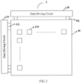
- FIG. 2 is a schematic diagram of a display panel provided by at least one embodiment of the present disclosure.
- the display panel is a display panel with a resolution of 8K and a refresh rate of 120Hz, or may be a display panel with other resolutions or refresh rates, which are not limited in the embodiments of the present disclosure.
- the display panel 1 includes a gate driving circuit 10.
- the display panel 1 further includes a display region 40, the display region 40 includes a pixel array connected to the gate driving circuit 10, and the pixel array includes a plurality of rows and a plurality of columns of sub-pixels 410.
- the display panel 1 further includes a data driving circuit 30 and a plurality of data lines DL.
- the plurality of data lines DL are electrically connected to the plurality of columns of sub-pixels 410 and configured to transmit data signals provided by the data driving circuit 30 to the plurality of columns of sub-pixels 410.
- the data driving circuit 30 is configured to provide data signals to the pixel array
- the gate driving circuit 10 is configured to provide gate scanning signals to the pixel array.
- the data driving circuit 30 is electrically connected to the sub-pixels 410 through a data line DL
- the gate driving circuit 10 is electrically connected to the sub-pixels 410 through a gate scanning signal line GL.
- the gate driving circuit is configured to drive a display panel such as a liquid crystal display panel, an organic light-emitting diode display panel, etc., and to sequentially provide gate scanning signals for a plurality of gate scanning signal lines of the display panel, so as to perform progressive scanning or interlaced scanning while the display panel displays one frame of pattern.
- a display panel such as a liquid crystal display panel, an organic light-emitting diode display panel, etc.
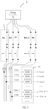
- FIG. 3 is a schematic diagram of another display panel provided by at least one embodiment of the present disclosure.
- the display panel 1 further includes a plurality of clock signal lines CLK1 to CLKm (m is an even number greater than 0), a timing controller 300, and a plurality of anti-cross-row circuits.
- CLK1 to CLKm m is an even number greater than 0
- a timing controller 300 a timing controller 300
- a plurality of anti-cross-row circuits for clarity and conciseness, the display region 40 and the data driving circuit 30 are not shown in FIG. 3 .
- FIG. 2 please refer to the description in FIG. 2 , which will not be repeated here.
- m may be equal to 2, 4, 6, 12, 16, etc., that is, the plurality of clock signal lines may include 2, 4, 6, 12, 16, etc., and the amount of clock signal lines is an integer multiple of 2, which are not limited in the embodiments of the present disclosure.
- the distance between the plurality of clock signal lines may be in a range from 4 ⁇ m to 100 ⁇ m, for example, form 4 ⁇ m to 20 ⁇ m, which are not limited in the embodiments of the present disclosure.
- the timing controller 300 is configured to provide a first clock signal.
- the plurality of anti-cross-row circuits 400 are connected with the timing controller 300 and the plurality of clock signal lines CLK1 to CLKm, and are configured to adjust the first clock signal provided by the timing controller 300 to a second clock signal, and output the second clock signal to the plurality of clock signal lines CLK1 to CLKm.
- the plurality of anti-cross-row circuits 400 are connected with the plurality of clock signal lines in one-to-one correspondence, that is, one clock signal line is connected to one anti-cross-row circuit 400, which are not limited in the embodiments of the present disclosure.
- the anti-cross-row circuit 400 may also be provided between the timing controller 300 and other power supply lines, for example, power supply lines that supply a first voltage to a fourth voltage to a first voltage terminal to a fourth voltage terminal shown in FIG. 10 , to reduce peak current, etc., which are not limited in the embodiments of the present disclosure.
- the gate driving circuit 10 includes a plurality of shift register units GOA that are cascaded, which are connected to the plurality of clock signal lines CLK1 to CLKm, respectively.
- the gate driving circuit 10 is configured to output the second clock signal as an output signal line by line, thereby shortening the falling duration of the falling edge of the output signal.
- the plurality of clock signal lines include a first clock signal line CLK1, a second clock signal line CLK2, a third clock signal line CLK3, a fourth clock signal line CLK4, a fifth clock signal line CLK5, a sixth clock signal line CLK6, a seventh clock signal line CLK7, an eighth clock signal line CLK8, a ninth clock signal line CLK9, a tenth clock signal line CLK10, an eleventh clock signal line CLK11, and a twelfth clock signal line CLK12.
- the first clock signal line CLK1 is connected to a clock signal terminal of a (12n-11)th-stage shift register;
- the second clock signal line CLK2 is connected to a clock signal terminal of a (12n-10)th-stage shift register-;
- the third clock signal line CLK3 is connected to a clock signal terminal of a (12n-9)th-stage shift register;
- the fourth clock signal line CLK4 is connected to a clock signal terminal of a (12n-8)th-stage shift register;
- the fifth clock signal line CLK5 is connected to a clock signal terminal of a (12n-7)th-stage shift register;
- the sixth clock signal line CLK6 is connected to a clock signal terminal of a (12n-6)th-stage shift register;
- the seventh clock signal line CLK7 is connected to a clock signal terminal of a (12n-5)th-stage shift register;
- the eighth clock signal line CLK8 is connected to a clock signal terminal of a (12n-4)th-stage shift register;
- connection mode between the clock signal lines of other numbers and the shift register units is similar to that of the 12 clock signal lines, which will not be repeated here; of course, other connection modes may also be used, which are not limited in the embodiments of the present disclosure.
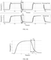
- FIG. 4A is a schematic diagram of a first clock signal and a second clock signal provided by at least one embodiment of the present disclosure
- FIG. 4B is a schematic diagram of an output signal output by a gate driving circuit before and after adding an anti-cross-row circuit 400 provided by at least one embodiment of the present disclosure.
- the upper and lower waveform diagrams are a comparison diagram of the first clock signal and the second clock signal at the proximal end of the timing controller 300 and a comparison diagram of the first clock signal and the second clock signal at the distal end of the timing controller 300, respectively.
- the falling duration t1 of the falling edge of the second clock signal (the waveform shown by the solid line in FIG. 4A ) is less than the falling duration t2 of the falling edge of the first clock signal (the waveform shown by the dotted line in FIG. 4A ).
- the solid line is the second clock signal output by the gate driving circuit and is used as the output signal
- the dotted line is the first clock signal output by the gate driving circuit and is used as the output signal.
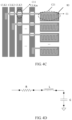
- FIG. 4C is a schematic diagram of a parasitic capacitance of a clock signal line according to at least one embodiment of the present disclosure.
- the capacitance load of the clock signal line CLK1 comes from a parasitic capacitance C11 generated at an overlap between a connection electrode E1 of the clock signal line CLK1 and the clock signal lines CLK2-CLKm connected to different shift register units, and a parasitic capacitance C21 generated at an overlap between a gate electrode of an output transistor (the third transistor T3 shown in FIG. 12 ) of the shift register unit and the connection electrode E1.
- the capacitive load e.g., parasitic capacitances C11 and C21
- the capacitive load of the clock signal line can be offset, so that the impedance of the clock signal is reduced, the falling duration of the falling edge of the clock signal is reduced, and the falling duration of the falling edge of the output signal is reduced, so that the occurrence of the cross-row phenomenon can be avoided.
- clock signal line CLK1 is taken as an example for description above, and other clock signal lines CLK2-CLKm are similar to the clock signal line CLK1, which will not be described here.
- each of the plurality of anti-cross-row circuits 400 includes at least one resistor and at least one inductor.
- at least one resistor and at least one inductor are connected in series or in parallel.
- the total resistance value of the equivalent resistance of each anti-cross-row circuit 400 is in a range from 1 ohm (S2) to 1000 ohm, and the total inductance of the equivalent inductance of each anti-cross-row circuit is in a range from 1 microhenry to 1000 microhenry.
- the total resistance value of the equivalent resistance of each anti-cross-row circuit 400 is 150 ⁇ , and the total inductance value of each equivalent inductance is 100 microhenry.
- a first end of the at least one resistor is connected to the timing controller 300, and a second end of the at least one resistor is connected to the at least one inductor.
- the anti-cross-row circuit 400 connected to the clock signal line CLK1 includes a resistor R1 and an inductor L1.
- the anti-cross-row circuit 400 connected to the clock signal line CLK2 includes a resistor R2 and an inductor L2;
- the anti-cross-row circuit 400 connected to the clock signal line CLK3 includes a resistor R3 and an inductor L3;
- the anti-cross-row circuit 400 connected to the clock signal line CLKm-1 includes a resistor Rm-1 and an inductor Lm-1;
- the anti-cross-row circuit 400 connected to the clock signal line CLKm includes a resistor Rm and an inductance Lm.
- the first ends of the resistors R1-Rm are connected to the timing controller 300, the second ends of the resistors R1-Rm are connected to the first ends of the inductors L1-LM, respectively, and the second ends of the inductors L1-LM are connected to the plurality of clock signal lines CLK1-CLKm in one-to-one correspondence, respectively.
- the resistance values of the above-mentioned resistors may be equal, for example, the resistance value of the resistor R1 is equal to the resistance value of the resistor R2, is equal to the resistance value of the resistor R3, is equal to the resistance value of the resistor Rm-1, is equal to the resistance value of the resistor Rm, for example, is equal to 150 ⁇ .
- the resistance values of the above-mentioned resistors may not be equal, for example, it may be determined according to the distance between the timing controller 300 and the clock signal line.
- the specific situation may depend on the actual situation, which are not limited in the embodiments of the present disclosure.
- the inductance value of each of the above-mentioned inductors may be equal, for example, the inductance value of the inductor L1 is equal to the inductance value of the inductor L2, is equal to the inductance value of the inductor L3, is equal to the inductance value of the inductor L3m-1, is equal to the inductance value of the inductor Lm, for example, is equal to 100 microhenry.
- the inductance value of each of the above-mentioned inductors may not be equal, for example, it may be determined according to the distance between the timing controller 300 and the clock signal line. The greater the distance between the timing controller 300 and the clock signal line, the smaller the inductance value.
- the inductance of the inductor L1 is smaller than the inductance of the inductor L2, and the inductance of the inductor L2 is smaller than the inductance of the inductor Lm.
- the specific situation may depend on the actual situation, which are not limited in the embodiments of the present disclosure.
- FIG. 3 only shows the case where the at least one resistor includes one resistor, the at least one inductor includes one inductor, and the resistor and the inductor are connected in series.
- the embodiments of the present disclosure are not limited to this, and may include more resistors and inductors.
- FIG. 4E is a schematic diagram of a plan view of a display panel according to at least one embodiment of the present disclosure.
- the display panel includes a display region 11 and a peripheral region 12 surrounding the display region 11.
- the peripheral region 12 includes the corner part 13.
- the display region 11 includes a plurality of pixels arranged in array for receiving output signals of the gate driving circuit as gate scanning signals for display.
- the peripheral region 12 includes structures such as the gate driving circuit 10 that drives the plurality of sub-pixels in the display region 11 to display, the plurality of clock signal lines, etc.
- the display panel further includes a circuit board 600.
- the timing controller 300 and the anti-cross-row circuit 400 are provided on the circuit board 600.
- the specific settings may refer to the settings in the art, and will not be described herein.
- the resistor R1 is connected in series on the clock signal line between the timing controller 300 and the inductor L1, which can reduce the temperature of the corner part of the display panel, and prevent the display panel from heating up seriously and causing blackening problem and fire hazards.
- the driving ability of the shift register unit GOA is strong, and the current on the clock signal line is large.
- the corner part of the display panel is densely wired due to the turn of the clock signal line wiring, and considering the frame, the temperature of the corner part is relatively high.
- the verification data test shows that when the display panel with the resolution of 8K and the refresh rate of 120Hz works, the temperature of the corner part can reach more than 70°C, and the temperature of the corner part of the display panel can be reduced to 50°C by connecting the resistor in series. Therefore, connecting the resistor in series on the clock signal line can reduce the temperature of the corner part of the display panel, improve the user experience, and prolong the service life of the display panel.
- the resistors and inductors connected in series are examples of including the least devices.
- the inductors are connected in parallel next to the resistors, and the resistors are connected in parallel next to the inductors, which both belong to the protection scope of the present disclosure, and are not limited in the embodiments of the present disclosure.
- FIG. 5 is a schematic diagram of another display panel provided by at least one embodiment of the present disclosure.
- at least one resistor includes a first resistor R1 and a second resistor R1'
- at least one inductor includes a first inductor L 1' and a second inductor L1.
- the first resistor R1 and the first inductor L1' are connected in parallel to form a first element 410
- the second resistor R1' and the second inductor L1 are connected in parallel to form a second element 420.
- the first element 410 and the second element 420 are connected in series.
- the first element 410 and the second element 420 may be equivalent to inductors, and the total inductance value of the equivalent inductance of the first element 410 and the equivalent inductance of the second element 420 is in a range from 1 microhenry to 1000 microhenry; alternatively, in other examples, in the case where the first element and the second element are equivalent to resistors, the total resistance value of the equivalent resistance of the first element and the equivalent resistance of the second element is in a range from 1 ohm to 1000 ohm.
- the first element 410 or the second element 420 may include a plurality of resistors which are connected in series or in parallel.
- the resistance value of the resistor is in a range from 1 ohm to 1000 ohm; and in the case where the anti-cross-row circuit 400 includes two resistors connected in parallel, the resistance value of each resistor may be 2000 ohm, so that the resistance value of the two resistors connected in parallel is 1000 ohm, as long as the resistance value of the equivalent resistance of the first element 410 or the equivalent resistance of the second element 420 (i.e., the total resistance value of the equivalent resistance of the anti-cross-row circuit 400) is in a range from 1 ohm to 1000 ohm, which are not limited in the embodiments of the present disclosure.
- the first element 410 or the second element 420 may include a plurality of inductors which are connected in series or in parallel.
- the inductance value of the inductor is in a range from 1 microhenry to 1000 microhenry; and when the anti-cross-row circuit 400 includes a plurality of inductors connected in series or in parallel, the resistance value of each inductor may be adjusted according to actual situations, as long as the total inductance value of the equivalent inductance of the first element 410 or the equivalent inductance of the second element 420 (i.e., the total inductance value of the equivalent inductance of the anti-cross-row circuit 400) is in a range from 1 microhenry to 1000 microhenry, which are not limited in the embodiments of the present disclosure.
- FIG. 4D is a schematic diagram of a circuit load model provided by at least one embodiment of the present disclosure.
- the display panel of the above-mentioned embodiment of the present disclosure can form an inductive load by connecting an inductor in series between the timing controller and the gate driving circuit to offset the capacitive load on the clock signal line, so that there is only the resistive load on the clock signal line, so as to prevent the parasitic capacitance on the clock signal line from prolonging the falling duration of the falling edge of the clock signal.
- the current on the clock signal line can be reduced, the heat generation of the clock signal line can be reduced, and the performance of the display panel can be improved.
- FIG. 6 is a schematic diagram of waveforms of a first clock signal and a second clock signal provided by at least one embodiment of the present disclosure
- FIG. 7 is a schematic diagram of waveforms of a second clock signal and an output signal provided by at least one embodiment of the present disclosure
- FIG. 8 is an enlarged schematic diagram of an output signal provided by at least one embodiment of the present disclosure.
- the waveform of the output signal output by the output terminal depends on an input waveform of the gate driving circuit, that is, depends on the waveform of the second clock signal provided by the clock signal line.
- the waveform of the second clock signal provided by the clock signal line includes multi-level levels, so that the waveform of the output signal output by the output terminal of the gate driving circuit also includes multi-level levels.
- the multi-level levels refer to one low level including multi-level low levels or one high level including multi-level high levels, which are not limited in the embodiments of the present disclosure.
- the second clock signal with multi-level levels can solve the problem that the falling duration of the falling edge of the output signal is long.
- the falling duration of the falling edge of the output signal is determined according to 10% (VGH-VGL1) to 90% (VGH-VGL1) of the falling edge of the output signal. Because the waveform of the output signal becomes multi-level levels, the falling edge of the output signal forms an undershoot, so the falling duration of the falling edge of the output signal becomes small.
- VGH is the first level as shown in FIG. 6
- VGL1 is the first voltage provided by the first voltage terminal as shown in FIG. 10 .
- the output noise reduction circuit 180 shown in FIG. 10 is turned on due to a low level output by the output terminal of the shift register unit, the first voltage provided by the first voltage terminal VGL1 is output to the output terminal. Therefore, the undershoot height of the falling edge is taken as VGH-VGL1.
- the first clock signal includes a first level VGH and a second level LVGL sequentially arranged in a time domain
- the second clock signal includes a third level VGH3 and a fourth level sequentially arranged in the time domain
- the first level VGH is higher than the second level LVGL
- the third level VGH3 is higher than the fourth level
- the fourth level includes a first sub-level LVGL1 and a second sub-level LVGL2
- the second sub-level LVGL2 is between the third level VGH3 and the first sub-level LVGL1.
- the second sub-level LVGL2 is lower than the first sub-level LVGL1, so that the falling edge of the second clock signal may form an undershoot from the third level VGH3 to the second sub-level LVGL2, thereby shortening the falling duration of the falling edge.
- the value range of the first sub-level and the second sub-level may be in the range from -4V to -20V, which depends on the actual situation and is not limit in the embodiments of the present disclosure.
- the first sub-level LVG1 is equal to the first voltage provided by the first voltage terminal VGL1 as shown in FIG. 10 , for example, both of them are -10V, and the second voltage provided by the second voltage terminal VGL2 as shown in FIG. 10 , for example, is -8V
- the specific situation may depend on the actual situation, which is not limited in the embodiments of the present disclosure.
- the first level VGH and the third level VGH3 are high levels, and the second level LVGL and the fourth level are low levels.
- the following embodiments are the same as this and will not be described again.
- the first level VGH and the third level VGH3 are equal or substantially equal, and the first sub-level LVGL1 and the second level LVGL are equal or substantially equal, which are not limited in the embodiments of the present disclosure.
- the gate driving circuit outputs the second clock signal as the output signal
- the falling edge of the output signal also forms an undershoot from the third level VGH3 to the second sub-level LVGL2, so that the falling duration of the falling edge of the output signal can be shortened, and the falling duration of the falling edge of the output signal is shortened from a first time (i.e., the falling duration is the distance between A1 and A3 in the horizontal direction) to a second time (i.e., the falling duration is the distance between A1 and A2 in the horizontal direction).
- FIG. 9 is a schematic diagram of another second clock signal provided by at least one embodiment of the present disclosure.
- the third level VGH3 includes a third sub-level VGH5 and a fourth sub-level VGH4.
- the fourth sub-level VGH4 is between the third sub-level VGH5 and the second sub-level LVGL2, that is, in the time domain, the third sub-level VGH5 precedes the fourth sub-level VGH4, the fourth sub-level VGH4 precedes the second sub-level LVGL2, and the second sub-level LVGL2 precedes the first sub-level LVGL1.
- the third sub-level VGH5 is higher than the fourth sub-level VGH4, so that when the third sub-level VGH5 of the second clock signal is output, according to the law of charge conservation of the capacitor, the voltage of the gate electrode (i.e., the N1 node as shown in FIG. 12 ) of the third transistor T3 may be increased, so that the third transistor T3 can be turned on more thoroughly.
- the voltage of the gate electrode i.e., the N1 node as shown in FIG. 12
- the fourth sub-level VGH4 and the first level VGH are equal or substantially equal, that is, the fourth sub-level VGH4 and the third level VGH3 are equal or substantially equal, which are not limited in the embodiments of the present disclosure.
- widths of the second sub-level LVGL2 and the third sub-level VGH5 may be 0.5H-m/2H, or 0.5H-2H, and 1H is the charging duration of one row of pixels.
- 1H is the charging duration of one row of pixels.
- the widths of the second sub-level LVGL2 and the third sub-level VGH5 may be less than or equal to 6H, that is, six times the charging duration of one row of sub-pixels.
- the specific width range may be determined according to the actual situation, which is not limited in the embodiments of the present disclosure.
- the waveform of the second clock signal may directly form a undershoot of VGH5-LVGL2 at the falling edge without adopting multi-level levels.
- the first clock signal includes the first level and the second level sequentially arranged in the time domain
- the second clock signal includes the third level and the fourth level sequentially arranged in the time domain.
- the first level is higher than the second level
- the third level is higher than the fourth level
- the second level is higher than the fourth level
- the third level is higher than the first level.
- the first level is VGH as shown in FIG. 6
- the second level is LVGL as shown in FIG. 6
- the third level is VGH5 as shown in FIG. 9
- the fourth level is LVGL2 as shown in FIG. 6 or FIG. 9 .
- the widths of the above-mentioned four levels are all m/2H.
- the falling edge of the waveform of the second clock signal forms the undershoot of VGH5-LVGL2, which is larger than the undershoot VGH-LVGL at the falling edge of the first clock signal, so that the falling duration of the falling edge is shortened.
- the first level VGH, the third level VGH3, the third sub-level VGH5 and the fourth sub-level VGH4 included in the third level VGH3, the third voltage provided by the third voltage terminal VGH1 as shown in FIG. 10 , and the fourth voltage provided by the fourth voltage terminal VGH2 as shown in FIG. 10 may all have the value range of 25V-40V
- the first level VGH is 32V
- the third sub-level VGH5 is 36V
- the fourth sub-level VGH4 is 32V
- the third level VGH3 is 32V, which can be determined according to the actual situation and are not limited in the embodiment of the present disclosure.
- the display panel further includes a level conversion circuit (not shown),which is configured to convert a logic level signal into the first clock signal or configured to convert the first clock signal into the above-mentioned second clock signal having a signal with multi-level levels shown in FIG. 6 or FIG. 9 .
- a level conversion circuit (not shown),which is configured to convert a logic level signal into the first clock signal or configured to convert the first clock signal into the above-mentioned second clock signal having a signal with multi-level levels shown in FIG. 6 or FIG. 9 .
- the level conversion circuit can convert a logic level into the first clock signal having a signal with multi-level levels, and then output the first clock signal to the anti-cross-row circuit 400, and the anti-cross-row circuit outputs the second clock signal having a signal with multi-level levels to the plurality of clock signal lines.
- the level conversion circuit can convert the first clock signal into the second clock signal having a signal with multi-level levels as shown in FIG. 6 or FIG. 9 , and then input the second clock signal to the anti-cross-row circuit.
- the second clock signal may be set as a signal with multi-level levels through the level conversion circuit and then the second clock signal having a signal with multi-level levels may be output to the plurality of clock signal lines, which are not limited in the embodiments of the present disclosure.
- the clock signal adopts a multi-level levels design of one high level with multi-level low levels or multi-level high levels with multi-level low levels, which can enable the second clock signal to form an undershoot to reduce the delay of the falling duration of the falling edge, thereby shortening the falling duration of the falling edge of the output signal. Therefore, the driving ability of the gate driving circuit can be enhanced to a certain extent, and can be used for driving all products, such as display products with a resolution of 4K, display products with a resolution of 8K, or COF (Chip On Flex or Chip On Film) products, etc.
- only the multi-level levels design of the clock signal is adopts and the driving ability of the shift register unit can enhanced to a certain extent.
- only resistors may be connected in series between the timing controller 300 and the plurality of signal lines, which can effectively reduce the current on the clock signal lines and greatly reduce the temperature at the corner part of the display panel.
- the display panel is applicable to products with a small number of clock signal lines but a high charging rate.
- the display panel is applicable to products whose charging rate needs to be increased and the GOE edge is insufficient, and may also be applicable to products with horizontal stripes on the pattern.
- the shift register unit may adopt a circuit structure in the art, for example, 4T1C, 10T4C, 21T1C, etc., which is not limited in the embodiments of the present disclosure, and the specific driving process may refer to conventional introduction in the art, and will not be described here.
- FIG. 10 is a schematic diagram of a shift register unit provided by an embodiment of the present disclosure.
- the shift register unit 500 includes an input circuit 110, an output circuit 120, a first node N1, and a first node control circuit 130.
- a gate driving circuit can be obtained by cascading a plurality of the shift register units 500.
- the gate driving circuit is configured to drive a display panel, and sequentially provide scanning signals to a plurality of gate lines of the display panel, so that the progressive scanning or interlaced scanning is performed during a period when the display panel displays a frame of pattern.
- the input circuit 110 is connected to the first node N1 (for example, a pull-up node here), and is configured to charge the first node N1 in response to an input signal.
- the input circuit 110 is connected to an input signal terminal INT and the first node N1, and is configured to be turned on under the control of the input signal provided by the input signal terminal INT, so as to enable the input signal terminal INT to be connected to the first node N1, so that the input signal provided by the input signal terminal INT is input to the first node N1, and the potential of the first node N1 is charged (e.g., pulled up) to an working potential.
- the output circuit 120 includes an output terminal OUT connected to the first node N1, and is configured to output an output signal at the output terminal OUT under the control of a level of the first node N1.
- the output circuit 120 is connected to a clock signal terminal CLK, the first node N1, and the output terminal OUT, and is configured to be turned on under the control of the level of the first node N1, transmit a second clock signal provided by the clock signal terminal CLK to the output terminal OUT, and the second clock signal is output as the output signal at the output terminal OUT.
- the output circuit 120 is further connected to a voltage terminal, and the second clock signal provided by the clock signal terminal CLK is used as a control signal to control whether the voltage terminal is connected to the output terminal OUT, thereby controlling whether a voltage signal of the voltage terminal is transmitted to the output terminal OUT and output as the output signal at the output terminal OUT.
- the clock signal terminal CLK is connected to one of clock signal lines CLK1-CLKm to receive the second clock signal, thereby outputting the second clock signal to the output terminal OUT as the output signal.
- the output terminal OUT may include a plurality of output terminals, such as a shift output terminal and at least one scanning signal output terminal, so as to output the output signal, such as the second clock signal provided by the clock signal terminal CLK, to the shift output terminal and the scanning signal output terminal, so as to improve the driving ability of the shift register unit 500.
- the at least one scanning signal output terminal includes one scanning signal output terminal.
- the shift output terminal is configured to provide an input signal and a reset signal to the next-stage shift register unit 500
- the scanning signal output terminal is configured to provide a driving signal to the pixel circuits of one row of pixel units in the display panel.
- each scanning signal output terminal may also output different output signals.
- the specific settings are determined according to the actual situation, which are not limited in the embodiments of the present disclosure.
- the first node control circuit 130 is connected to the second node N2 and the third node N3, respectively, and is configured to control levels of the second node N2 and the third node N3 in response to the input signal.
- the first node control circuit 130 is configured to be connected to the second node N2, the third node N3, a second voltage terminal VGL2 (for example, providing a low level) or a separately provided voltage terminal (for example, a low voltage terminal) and the input terminal INT, so that the second node N2 and the third node N3 are electrically connected to the second voltage terminal VGL2 or the low voltage terminal under the control of the input signal input by the input terminal INT, so as to ensure that the levels of the second node N2 and the third node N3 are pulled down to a second voltage at the stage of pulling up the first node N1.
- active output level of the shift register unit refers to a level at which a switching transistor in the pixel circuit of the display panel connected to the shift register unit can be turned on so that a data signal can be written into the pixel circuit.
- active output level refers to a level that cannot cause the switching transistor in the pixel circuit connected to the shift register unit to be turned on (ie, the switching transistor is turned off).
- the active output level is higher or lower than the inactive output level depending on factors such as the type (N-type or P-type) of the switching transistor in the pixel circuit.
- the shift register unit outputs a square wave pulse signal at the output terminal during working, the active output level corresponds to the level of a square wave pulse part of the square wave pulse signal, and the inactive output level corresponds to the level of a non-square wave pulse part.
- the shift register unit further includes a first node reset circuit 150.
- the first node reset circuit 150 is connected to the first node N1 and is configured to reset the first node N1 in response to a reset signal.
- the first node reset circuit 150 is configured to be connected to the first node N1, the second voltage terminal VGL2 (e.g., providing a low level) or a separately provided voltage terminal (e.g., a low voltage terminal), and a reset terminal RST, so that the first node N1 is electrically connected to the second voltage terminal VGL2 or the low voltage terminal under the control of the reset signal input from the reset terminal RST, so as to perform pulling-down and resetting operations on the first node N1.
- the shift register unit 500 further includes a second node control circuit 160, a first node noise reduction circuit 170, and an output noise reduction circuit 180.
- the second node control circuit 160 is connected to the first node N1, the second node N2, and the third node N3, and is configured to control levels of the second node N2 and the third node N3 under the control of the level of the first node N1.
- the second node control circuit 160 is connected to the first node N1, the second node N2, the third node N3, the second voltage terminal VGL2, the third voltage terminal VGH1, and the fourth voltage terminal VGH2 or a separately provided voltage terminal (for example, a high voltage terminal), thereby pulling down the levels of the second node N2 and the third node N3 to a low level.
- the second node N2 and the third node N3 are connected to one of the third voltage terminal VGH1 or the fourth voltage terminal VGH2.
- the first node N1 is at a high level
- the second node N2 and the third node N3 are connected to the second voltage terminal VGL2 or a separately provided voltage terminal (for example, a low voltage terminal), thereby pulling down the second node N2 and the third node N3 to a low level.
- the level of the second node N2 is controlled by the level of the first node N1 and a third voltage provided by the third voltage terminal VGH1
- the level of the third node N3 is controlled by the level of the first node N1 and a fourth voltage provided by the fourth voltage terminal VGH2.
- the third voltage terminal VGH1 and the fourth voltage terminal VGH2 may be set to alternately input a high level, that is, when the third voltage terminal VGH1 inputs a high level, the fourth voltage terminal VGH1 inputs a low level, and when the third voltage terminal VGH1 inputs a low level, the fourth voltage terminal VGH2 inputs a high level.
- the second node N2 and the third node N3 work alternately so that the transistors connected thereto can work alternately, thereby prolonging service life of these transistors.
- the third voltage terminal VGH1 and the fourth voltage terminal VGH2 may be replaced by a clock signal terminal that alternately provides a high level (a DC(Direct Current) low level when the implemented transistors are P-type), which is not limited in the embodiments of the present disclosure.
- the first node noise reduction circuit 170 is connected to the first node N1, the second node N2, and the third node N3, and is configured to perform noise reduction on the first node N1 under the control of levels of the second node N2 and the third node N3.
- the first node noise reduction circuit 170 is connected to the first node N1, the second node N2, the third node N3, and the second voltage terminal VGL2, and is configured to be turned on when the second node N2 and the third node N3 are, for example, at a high level, so that the first node N1 is connected to the second voltage terminal VGL2 or a separately provided voltage terminal (for example, a low voltage terminal), and the potential of the first node N1 is pulled down to a non-working potential to achieve noise reduction on the first node N1.
- the output noise reduction circuit 180 is connected to the second node N2, the third node N3, and the output terminal OUT, and is configured to perform noise reduction on the output terminal OUT under the control of the levels of the second node N2 and the third node N3.
- the output noise reduction circuit 180 is connected to the second node N2, the third node N3, the second voltage terminal VGL2, and the output terminal OUT, and is configured to be turned on when the second node N2 is, for example, at a high level, so that the output terminal OUT is connected to the second voltage terminal VGL2 or a separately provided voltage terminal (for example, a low voltage terminal) to achieve noise reduction on the output terminal OUT.
- the shift register unit 500 further includes a total reset circuit 190.
- the total reset circuit 190 is connected to the first node N1 and is configured to reset the first node N1 in response to a total reset signal.
- the total reset circuit 190 is configured to be connected to the first node N1, the second voltage terminal VGL2 (for example, providing a low level) or a separately provided voltage terminal (for example, a low voltage terminal), and a total reset terminal TRST, so that the first node N1 is connected to the second voltage terminal VGL2 or a low voltage terminal under the control of the total reset signal input by the total reset terminal TRST to perform pulling-down and resetting operations on the first node N1.
- the first voltage terminal VGL1 is configured to provide a DC low-level signal (e.g., lower than or equal to the low-level portion of the clock signal), such as connected to ground.
- a DC low-level signal e.g., lower than or equal to the low-level portion of the clock signal
- the DC low-level signal is referred to as the first voltage.
- the following embodiments are the same as this and will not be described again.
- the second voltage terminal VGL2 is configured to provide a DC low-level signal (for example, lower than or equal to the low-level portion of the clock signal), such as connected to ground.
- a DC low-level signal for example, lower than or equal to the low-level portion of the clock signal
- the DC low-level signal is referred to as the second voltage.
- the second voltage is lower than or equal to the first voltage, and the following embodiments are the same as this and will not be described again.
- the third voltage terminal VGH1 is configured to provide a DC high-level signal, and the signal provided by the third voltage terminal VGH1 is referred to as the third voltage.
- the fourth voltage terminal VGH2 is also configured to provide a DC high-level signal, and the signal provided by the fourth voltage terminal VGH2 is referred to as the fourth voltage.
- the third voltage and the fourth voltage may be the same voltage, and both are greater than the first voltage and the second voltage. The following embodiments are the same as this and will not be described again.
- FIG. 11 is a circuit diagram of a specific implementation example of the shift register unit shown in FIG. 10 .
- the shift register unit 500 includes a second to twenty-ninth transistors T2-T29, and further includes a storage capacitor C. It should be noted that in the following descriptions, each transistor is described as an N-type transistor, but this does not constitute a limitation on the embodiments of the present disclosure.
- the input circuit 110 may be implemented as a fourth transistor T4.
- the gate electrode and the first electrode of the fourth transistor T4 are electrically connected to each other, and are configured to be connected to the input terminal INT to receive the input signal, and the second electrode of the fourth transistor T4 is configured to be connected to the first node N1, so that when the fourth transistor T4 is turned on due to a turn-on signal (e.g., a high-level signal) received by the input terminal INT, the turn-on signal is used to charge the first node N1 to make the first node N1 at a high level.
- a turn-on signal e.g., a high-level signal
- the gate electrode and the first electrode of the fourth transistor T4 are connected to the input terminal INT or other high voltage terminals (for example, the third voltage terminal VGH1 or the fourth voltage terminal VGH2), respectively, which are not limited in the embodiments of the present disclosure.
- the output circuit 120 may be implemented to include a second transistor T2, a third transistor T3 and a storage capacitor C.
- the gate electrode of the second transistor T2 is connected to the first node N1, the first electrode of the second transistor T2 is connected to the clock signal terminal CLK to receive the second clock signal, and the second electrode of the second transistor T2 is connected to the shift output terminal CR.
- the gate electrode of the third transistor T3 is connected to the first node N1, the first electrode of the third transistor T3 is connected to the clock signal terminal CLK to receive the second clock signal, and the second electrode of the third transistor T3 is connected to the scanning signal output terminal OUT1 (i.e., the output terminal Gout shown in FIG. 3 ).
- the first electrode of the storage capacitor C is connected to the first node N1, and the second electrode of the storage capacitor C is connected to the scanning signal output terminal OUT1. It should be noted that, not limited to this, the shift register unit may further include more output signals and corresponding scanning signal output terminals.
- the clock signal terminal CLK is connected to one of the clock signal lines CLK1-CLKm shown in FIG. 3 to receive the second clock signal in the above-mentioned embodiments.
- the first node control circuit 130 may be implemented to include a fourteenth transistor T14 and a twenty-fourth transistor T24.
- the gate electrode of the fourteenth transistor T14 is connected to the input terminal INT to receive the input signal, the first electrode of the fourteenth transistor T14 is connected to the second node N2, and the second electrode of the fourteenth transistor T14 is connected to the second voltage terminal VGL2.
- the gate electrode of the twenty-fourth transistor T24 is connected to the input terminal INT to receive the input signal, the first electrode of the twenty-fourth transistor T24 is connected to the third node N3, and the second electrode of the twenty-fourth transistor T24 is connected to the second voltage terminal VGL2.
- the first node reset circuit 150 may be implemented as a fifth transistor T5.
- the gate electrode of the fifth transistor T5 is configured to be connected to the reset terminal RST to receive the reset signal, the first electrode of the fifth transistor T5 is connected to the first node N1, and the second electrode of the fifth transistor T5 is connected to the second voltage terminal VGL2 to receive the second voltage.
- the fifth transistor T5 is turned on in response to the reset signal, the first node N1 is electrically connected to the second voltage terminal VGL2, so that the reset operation is performed on the first node N1.
- the reset terminal RST is connected to the output terminal of the shift register that is cascaded with the reset terminal RST to realize real-time reset of the first node N1 of the shift register unit of the stage during the shift outputting process of the gate scanning signals, so as to avoid erroneous output of the output terminal.
- the total reset circuit 190 may be implemented as a sixth transistor T6.
- the gate electrode of the sixth transistor T6 is connected to the total reset terminal TRST to receive the total reset signal
- the first electrode of the sixth transistor T6 is connected to the first node N1
- the second electrode of the sixth transistor T6 is connected to the second voltage terminal VGL2 to receive the second voltage.
- the first node N1 is electrically connected to the second voltage terminal VGL2, so that the reset operation is performed on first node N1.
- the total reset circuit 190 is configured to globally reset all the shift register units that are cascaded during a start stage of the display stage of one frame of image or during an end stage of the display stage of one frame of image.
- the timing of the total reset signal is earlier than a trigger signal (which will be described in detail later) which controls the start stage of the display stage of one frame of image, so that first nodes N1 of all shift register units can be reset during the start stage of the display stage of one frame of image to avoid abnormality of the display pattern.
- a trigger signal which will be described in detail later
- the second node control circuit 160 may be implemented to include a seventh transistor T7, an eighth transistor T8, a ninth transistor T9, and a tenth transistor T10.
- the gate electrode of the seventh transistor T7 is connected to a first control node CN1, the first electrode of the seventh transistor T7 is connected to the third voltage terminal VGH1 to receive the third voltage, and the second electrode of the seventh transistor T7 is connected to the second node N2; the gate electrode of the eighth transistor T8 is connected to the first node N1, the first electrode of the eighth transistor T8 is connected to the second node N2, and the second electrode of the eighth transistor T8 is connected to the second voltage terminal VGL2 to receive the second voltage.
- the gate electrode and the first electrode of the ninth transistor T9 are electrically connected to each other, and are configured to be both connected to the third voltage terminal VGH1 to receive the third voltage, and the second electrode of the ninth transistor T9 is connected to the first control node CN1; the gate electrode of the tenth transistor T10 is connected to the first node N1, the first electrode of the tenth transistor T10 is connected to the first control node CN1, and the second electrode of the tenth transistor T10 is connected to the second voltage terminal VGL2 to receive the second voltage.
- the second node control circuit 160 further includes a twenty-seventh transistor T27, a twenty-eighth transistor T28, a twenty-ninth transistor T29, and a twentieth transistor T20.
- the gate electrode of the twenty-seventh transistor T27 is connected to the second control node CN2, the first electrode of the twenty-seventh transistor T27 is connected to the fourth voltage terminal VGH2 to receive the fourth voltage, and the second electrode of the twenty-seventh transistor T27 is connected to the third node N3;
- the gate electrode of the twenty-eighth transistor T28 is connected to the first node N1, the first electrode of the twenty-eighth transistor T28 is connected to the third node N3, and the second electrode of the twenty-eighth transistor T28 is connected to the second voltage terminal VGL2 to receive the second voltage.
- the gate electrode and the first electrode of the twenty-ninth transistor T29 are electrically connected to each other, and are configured to be both connected to the fourth voltage terminal VGH2 to receive the fourth voltage, and the second electrode of the twenty-ninth transistor T29 is connected to the second control node CN2; the gate electrode of the twentieth transistor T20 is connected to the first node N1, the first electrode of the twentieth transistor T20 is connected to the second control node CN2, and the second electrode of the twentieth transistor T20 is connected to the second voltage terminal VGL2 to receive the second voltage.
- the first node noise reduction circuit 170 may be implemented to include an eleventh transistor T11 and a twenty-first transistor T21.
- the gate electrode of the eleventh transistor T11 is connected to the second node N2, the first electrode of the eleventh transistor T11 is connected to the first node N1, and the second electrode of the eleventh transistor T11 is connected to the second voltage terminal VGL2 to receive the second voltage.
- the eleventh transistor T11 is turned on when the second node N2 is at a high potential, so as to connect the first node N1 and the second voltage terminal VGL2, so that the first node N1 can be pulled down to achieve noise reduction.
- the gate electrode of the twenty-first transistor T21 is connected to the third node N3, the first electrode of the twenty-first transistor is connected to the first node N1, and the second electrode of the twenty-first transistor is connected to the second voltage terminal VGL2 to receive the second voltage.
- the twenty-first transistor T21 is turned on when the third node N3 is at a high potential, so as to connect the first node N1 and the second voltage terminal VGL2, so that the first node N1 can be pulled down to achieve noise reduction.
- the eleventh transistor T11 and the twenty-first transistor T21 alternately work under the control of levels of the second node N2 and the third node N3, respectively, to prolong service life of these transistors.
- the output terminal OUT includes a shift output terminal CR and a scanning signal output terminal OUT1 (i.e., the output terminal Gout of the gate driving circuit), and the output noise reduction circuit 180 may be implemented to include a twelfth transistor T12, a twenty-second transistor T22, a thirteenth transistor T13, and a twenty-third transistor T23.
- the twelfth transistor T12 and the twenty-second transistor T22 are configured for noise reduction of the shift output terminal CR
- the thirteenth transistor T13 and the twenty-third transistor T23 are configured for noise reduction of the scanning signal output terminal OUT1.
- the output noise reduction circuit 180 may further include more transistors to achieve noise reduction on the scanning signal output terminals.
- the gate electrode of the twelfth transistor T12 is connected to the second node N2, the first electrode of the twelfth transistor T12 is connected to the shift output terminal CR, and the second electrode of the twelfth transistor T12 is connected to the second voltage terminal VGL2 to receive the second voltage.
- the twelfth transistor T12 is turned on when the second node N2 is at a high potential, so as to connect the shift output terminal CR and the second voltage terminal VGL2, thereby reducing noise on the shift output terminal CR.
- the gate electrode of the twenty-second transistor T22 is connected to the third node N3, the first electrode of the twenty-second transistor T22 is connected to the shift output terminal CR, and the second electrode of the twenty-second transistor T22 is connected to the second voltage terminal VGL2 to receive the second voltage.
- the twenty-second transistor T22 is turned on when the third node N3 is at a high potential, so as to connect the shift output terminal CR and the second voltage terminal VGL2, thereby reducing noise on the shift output terminal CR.
- the twelfth transistor T12 and the twenty-second transistor T22 alternately work under the control of the levels of the second node N2 and the third node N3, respectively, to prolong service life of these transistors.
- the gate electrode of the thirteenth transistor T13 is connected to the second node N2, the first electrode of the thirteenth transistor T13 is connected to the scanning signal output terminal OUT1, and the second electrode of the thirteenth transistor T13 is connected to the first voltage terminal VGL1 to receive the first voltage.
- the thirteenth transistor T13 is turned on when the second node N2 is at a high potential, so as to connect the scanning signal output terminal OUT1 and the first voltage terminal VGL1, thereby reducing noise on the scanning signal output terminal OUT1.
- the gate electrode of the twenty-third transistor T23 is connected to the third node N3, the first electrode of the twenty-third transistor T23 is connected to the scanning signal output terminal OUT1, and the second electrode of the twenty-third transistor T23 is connected to the first voltage terminal VGL1 to receive the first voltage.
- the twenty-third transistor T23 is turned on when the third node N3 is at a high potential, so as to connect the scanning signal output terminal OUT1 and the first voltage terminal VGL1, thereby reducing noise on the scanning signal output terminal OUT1.
- the thirteenth transistor T13 and the twenty-third transistor T23 alternately work under the control of the levels of the second node N2 and the third node N3, respectively, to prolong service life of these transistors.
- the term "pull-up” means charging a node or an electrode of a transistor to allow the absolute value of the level of the node or the electrode to be increased, thereby realizing an operation (e.g., turning on) of the corresponding transistor; and the term “pull-down” means discharging a node or an electrode of a transistor to reduce the absolute value of the level of the node or the electrode, thereby realizing an operation (e.g., turning off) of the corresponding transistor.
- the term "pull-up” means discharging a node or an electrode of a transistor o allow the absolute value of the level of the node or the electrode to be reduced, thereby realizing an operation (e.g., turning on) of the corresponding transistor; and the term “pull down” means charging a node or an electrode of a transistor to allow the absolute value of the level of the node or the electrode to be increased, thereby realizing an operation (e.g., turning off) of the corresponding transistor.
- first node N1, the second node N2, the third node N3, the first control node CN1 and the second control node CN2 do not represent actual components, but represent junction points of relevant electrical connections in the circuit diagram.
- each of the transistors used in the embodiments of the present disclosure may be a thin film transistor, a field effect transistor or other switching component having the same characteristics.
- the thin film transistor is taken as an example for description.
- the source electrode and drain electrode of the transistor used here may be structurally symmetrical, so that the source electrode and the drain electrode may be structurally indistinguishable.
- one electrode is directly described as the first electrode, and the other electrode is described as the second electrode.
- the transistors in the embodiments of the present disclosure are all described by taking N-type transistors as an example.
- the first electrode of the transistor is the drain electrode
- the second electrode is the source electrode.
- the present disclosure includes but is not limited to this.
- one or more transistors in the shift register unit 500 provided by the embodiments of the present disclosure may also adopt P-type transistors.
- the first electrode of the transistor is the source electrode
- the second electrode is the drain electrode.
- indium gallium zinc oxide may be adopted as an active layer of the thin film transistor, and compared with the adopting of low temperature polysilicon (LTPS) or amorphous silicon (for example, hydrogenated amorphous silicon) as the active layer of the thin film transistor, the size of the transistor can be effectively reduced and leakage current can be prevented.
- LTPS low temperature polysilicon
- amorphous silicon for example, hydrogenated amorphous silicon
- FIG. 12 is a driving timing diagram of a shift register unit provided by at least one embodiment of the present disclosure.
- the level of a potential in the signal timing diagram as shown in FIG. 12 is only schematic and does not represent the true potential value or relative ratio.
- the high-level signal corresponds to a turn-on signal of the N-type transistor
- the low-level signal corresponds to a turn-off signal of the N-type transistor.
- the working principle of the (N)th-stage shift register unit 500 of the gate driving circuit 10 as shown in FIG. 11 will be described below.
- the working principle of the shift register unit 500 is as follows.
- the input terminal INT provides a high level
- the clock signal terminal CLK provides a low level of the second clock signal. Therefore, the fourth transistor T4 is turned on, and the first node N1 is charged to a first high level. Meanwhile, the fourteenth transistor T14 and the twenty-fourth transistor T24 are turned on, so that the second node N2 and the third node N3 are pulled down to a low level.
- the second transistor T2 and the third transistor T3 are turned on in response to the first high level of the first node N1, thereby outputting the low level of the second clock signal provided by the clock signal terminal CLK to the shift output terminal CR and the scanning signal output terminal OUT1.
- the input terminal INT inputs a low level
- the clock signal terminal CLK provides a high level of the second clock signal
- the second electrode of the storage capacitor C is changed from a low level to a high level
- the voltage of the first electrode (i.e., the first node N1) of the storage capacitor C is bootstrapped according to the characteristic that the voltage at both ends of the capacitor cannot change suddenly. Therefore, in the second stage 2, the first node N1 is charged to a second high level, so that the second transistor T2 and the third transistor T3 are turned on in response to the second high level of the first node N1.
- the shift output terminal CR and the scanning signal output terminal OUT1 of the shift register unit output a high level.
- the voltage of the first electrode (i.e., the first node N1) of the storage capacitor C is bootstrapped according to the characteristic that the voltage at both ends of the capacitor cannot change suddenly. Therefore, in the second stage 2, the first node N1 is charged to a third sub-level VGHS, so that the level of the first node N1 is bootstrapped higher, so that the second transistor T2 and the third transistor T3 can be turned on more thoroughly, thereby facilitating the output of the second clock signal.
- the clock signal terminal CLK provides the low level of the second clock signal
- the second electrode of the storage capacitor C changes from the high level to the low level
- the voltage of the first electrode of the storage capacitor C i.e., the first node N1
- the second transistor T2 and the third transistor T3 are turned on in response to the first high level of the first node N1, and the shift output terminal CR and the scanning signal output terminal OUT1 of the shift register unit output the low level of the second clock signal.
- the reset terminal RST provides a high level of the reset signal. Therefore, the fifth transistor T5 is turned on, so that the first node N1 is connected to the second voltage terminal VGL2, so that the level of the first node N1 is changed to a low level, and the levels of the second node N2 and the third node N3 are changed to a high level.
- the second transistor T2 and the third transistor T3 are turned off in response to the low level of the first node N1, and the twelfth transistor T12, the twenty-second transistor T22, the thirteenth transistor T13, and the twenty-third transistor T23 are turned on, so that the shift output terminal CR and the scanning signal output terminal OUT1 of the shift register unit output a low level.
- the total reset terminal TRST provides a high level of the total reset signal, so that the sixth transistor T6 is turned on, and thus the first nodes N1 of all the shift register units of the gate driving circuit can be reset.
- FIG. 13 is a schematic diagram of a display device provided by at least one embodiment of the present disclosure.
- the display device 100 includes the display panel 1 provided by any embodiment of the present disclosure.
- the display device 100 in the embodiment may be any product or component with a display function, such as a liquid crystal panel, a liquid crystal TV, a display, an OLED panel, an OLED TV, an electronic paper display device, a mobile phone, a tablet computer, a notebook computer, a digital photo frame, a navigator, etc.
- the display device 100 may further include other conventional components such as a display panel, which is not limited in the embodiments of the present disclosure.
- the technical effects of the display device 100 according to the embodiments of the present disclosure may refer to the corresponding descriptions on the display panel in the above-mentioned embodiments, and details are not repeated here.
Landscapes
- Engineering & Computer Science (AREA)
- Physics & Mathematics (AREA)
- Computer Hardware Design (AREA)
- General Physics & Mathematics (AREA)
- Theoretical Computer Science (AREA)
- Chemical & Material Sciences (AREA)
- Crystallography & Structural Chemistry (AREA)
- Control Of Indicators Other Than Cathode Ray Tubes (AREA)
- Liquid Crystal (AREA)
- Liquid Crystal Display Device Control (AREA)
- Control Of El Displays (AREA)
Applications Claiming Priority (2)
| Application Number | Priority Date | Filing Date | Title |
|---|---|---|---|
| CN202110594338.4A CN115410506A (zh) | 2021-05-28 | 2021-05-28 | 显示面板及显示装置 |
| PCT/CN2021/126858 WO2022247135A1 (zh) | 2021-05-28 | 2021-10-28 | 显示面板及显示装置 |
Publications (2)
| Publication Number | Publication Date |
|---|---|
| EP4207151A1 true EP4207151A1 (de) | 2023-07-05 |
| EP4207151A4 EP4207151A4 (de) | 2024-05-08 |
Family
ID=84155218
Family Applications (1)
| Application Number | Title | Priority Date | Filing Date |
|---|---|---|---|
| EP21942699.6A Pending EP4207151A4 (de) | 2021-05-28 | 2021-10-28 | Anzeigetafel und anzeigevorrichtung |
Country Status (5)
| Country | Link |
|---|---|
| US (1) | US12087204B2 (de) |
| EP (1) | EP4207151A4 (de) |
| JP (1) | JP2024522249A (de) |
| CN (1) | CN115410506A (de) |
| WO (1) | WO2022247135A1 (de) |
Families Citing this family (6)
| Publication number | Priority date | Publication date | Assignee | Title |
|---|---|---|---|---|
| WO2024234304A1 (zh) * | 2023-05-16 | 2024-11-21 | 京东方科技集团股份有限公司 | 显示装置、栅极驱动电路、移位寄存单元及其驱动方法 |
| TWI863414B (zh) * | 2023-07-11 | 2024-11-21 | 友達光電股份有限公司 | 閘極驅動電路及應用其之顯示面板 |
| CN117037736B (zh) * | 2023-08-31 | 2026-04-03 | 长沙惠科光电有限公司 | 液晶显示面板和液晶显示器 |
| CN117672109B (zh) * | 2023-12-13 | 2024-12-06 | 长沙惠科光电有限公司 | 显示面板的驱动电路、显示面板及显示装置 |
| KR20250104547A (ko) * | 2023-12-29 | 2025-07-08 | 엘지디스플레이 주식회사 | 표시장치 및 이의 구동방법 |
| CN119107917A (zh) * | 2024-10-25 | 2024-12-10 | 厦门天马光电子有限公司 | 显示面板、驱动芯片及显示装置 |
Family Cites Families (31)
| Publication number | Priority date | Publication date | Assignee | Title |
|---|---|---|---|---|
| US5532553A (en) | 1994-10-19 | 1996-07-02 | Hubbell Incorporated | Operating circuit for electroluminescent panel |
| JP2002215104A (ja) * | 2001-01-15 | 2002-07-31 | Matsushita Electric Ind Co Ltd | マトリクス型表示装置とその駆動方法及び携帯情報端末 |
| KR100951901B1 (ko) * | 2003-08-14 | 2010-04-09 | 삼성전자주식회사 | 신호 변환 장치 및 이를 갖는 표시 장치 |
| US8552778B2 (en) | 2009-09-24 | 2013-10-08 | Freescale Semiconductor, Inc. | Duty cycle corrector and duty cycle correction method |
| TWI384756B (zh) | 2009-12-22 | 2013-02-01 | Au Optronics Corp | 移位暫存器 |
| CN101916540B (zh) * | 2010-08-10 | 2012-08-29 | 友达光电股份有限公司 | 时钟脉冲信号产生方法 |
| CN103514843A (zh) * | 2012-06-25 | 2014-01-15 | 群康科技(深圳)有限公司 | 非晶硅整合栅极驱动电路 |
| CN103475341B (zh) | 2013-09-16 | 2016-06-08 | 北京京东方光电科技有限公司 | 时钟信号生成方法及生成电路、栅极驱动电路 |
| WO2015136588A1 (ja) * | 2014-03-13 | 2015-09-17 | 株式会社Joled | El表示装置 |
| CN106033658A (zh) | 2015-03-18 | 2016-10-19 | 群创光电股份有限公司 | 显示器装置 |
| CN104810058B (zh) * | 2015-05-13 | 2018-04-06 | 京东方科技集团股份有限公司 | 移位寄存器及其驱动方法、栅极驱动电路和显示装置 |
| CN104867472B (zh) | 2015-06-15 | 2017-10-17 | 合肥京东方光电科技有限公司 | 一种移位寄存器单元、栅极驱动电路和显示装置 |
| CN105702194B (zh) * | 2016-04-26 | 2019-05-10 | 京东方科技集团股份有限公司 | 一种移位寄存器单元、栅极驱动电路及其驱动方法 |
| CN205984239U (zh) * | 2016-07-29 | 2017-02-22 | 华南理工大学 | 一种行扫描驱动单元和行扫描驱动系统 |
| KR102376490B1 (ko) * | 2017-03-29 | 2022-03-18 | 삼성디스플레이 주식회사 | 표시 장치 |
| CN108847195A (zh) | 2018-06-29 | 2018-11-20 | 深圳市华星光电半导体显示技术有限公司 | 降低阵列基板行驱动电流的电路及方法和液晶显示器 |
| CN110880304B (zh) * | 2018-09-06 | 2022-03-04 | 合肥鑫晟光电科技有限公司 | 移位寄存器单元、栅极驱动电路、显示装置及驱动方法 |
| CN109243356A (zh) | 2018-10-23 | 2019-01-18 | 惠科股份有限公司 | 驱动电路、显示装置及显示装置的驱动方法 |
| CN109448624B (zh) * | 2018-12-03 | 2020-10-13 | 深圳市华星光电半导体显示技术有限公司 | Goa电路及显示面板 |
| KR102614690B1 (ko) * | 2018-12-26 | 2023-12-19 | 삼성디스플레이 주식회사 | 표시 장치 |
| CN109448628B (zh) * | 2019-01-04 | 2022-04-12 | 合肥京东方光电科技有限公司 | 一种栅极驱动电路及其驱动方法 |
| CN111971737B (zh) * | 2019-03-01 | 2022-05-31 | 京东方科技集团股份有限公司 | 移位寄存器单元、栅极驱动电路、显示装置及驱动方法 |
| CN109979408A (zh) | 2019-04-29 | 2019-07-05 | 深圳市华星光电技术有限公司 | 过流保护电路、方法及显示设备 |
| CN111599323B (zh) | 2020-02-19 | 2022-07-05 | 京东方科技集团股份有限公司 | 移位寄存器及驱动方法、栅极驱动电路 |
| CN111240114B (zh) * | 2020-03-16 | 2021-06-01 | 深圳市华星光电半导体显示技术有限公司 | 阵列基板及液晶显示面板 |
| CN111653243B (zh) * | 2020-06-23 | 2022-02-08 | 上海天马微电子有限公司 | 驱动电路、背光结构、显示面板、显示装置及驱动方法 |
| CN111754923B (zh) | 2020-07-10 | 2021-09-24 | 武汉华星光电技术有限公司 | Goa电路以及显示面板 |
| CN112216249B (zh) * | 2020-10-20 | 2022-05-20 | 京东方科技集团股份有限公司 | 栅极驱动电路及显示装置 |
| CN112419994B (zh) | 2020-11-30 | 2022-07-12 | 厦门天马微电子有限公司 | 显示面板和显示装置 |
| CN112687229B (zh) | 2021-01-29 | 2022-10-14 | 云谷(固安)科技有限公司 | 移位寄存器和栅极驱动电路 |
| CN215834233U (zh) * | 2021-05-28 | 2022-02-15 | 北京京东方显示技术有限公司 | 显示面板及显示装置 |
-
2021
- 2021-05-28 CN CN202110594338.4A patent/CN115410506A/zh active Pending
- 2021-10-28 EP EP21942699.6A patent/EP4207151A4/de active Pending
- 2021-10-28 JP JP2023524426A patent/JP2024522249A/ja active Pending
- 2021-10-28 US US17/912,952 patent/US12087204B2/en active Active
- 2021-10-28 WO PCT/CN2021/126858 patent/WO2022247135A1/zh not_active Ceased
Also Published As
| Publication number | Publication date |
|---|---|
| JP2024522249A (ja) | 2024-06-12 |
| US12087204B2 (en) | 2024-09-10 |
| US20240212563A1 (en) | 2024-06-27 |
| EP4207151A4 (de) | 2024-05-08 |
| WO2022247135A1 (zh) | 2022-12-01 |
| CN115410506A (zh) | 2022-11-29 |
Similar Documents
| Publication | Publication Date | Title |
|---|---|---|
| US11749158B2 (en) | Shift register unit, gate driving circuit, display device, and driving method | |
| US12087204B2 (en) | Display panel and display device | |
| US11328672B2 (en) | Shift register unit and driving method thereof, gate driving circuit, and display device | |
| US11244595B2 (en) | Shift register unit comprising input circuit, first control circuit, blanking control circuit, first output circuit, and second output circuit, driving method, gate driving circuit, and display device | |
| US11263953B2 (en) | Shift register unit and drive method thereof, gate drive circuit and display device | |
| US11302276B2 (en) | Gate drive circuit, touch display device and driving method | |
| US11127478B2 (en) | Shift register unit and driving method thereof, gate driving circuit, and display device | |
| US11295645B2 (en) | Shift register and driving method thereof, gate driving circuit and display apparatus | |
| CN215834233U (zh) | 显示面板及显示装置 | |
| EP3944223A1 (de) | Schieberegistereinheit, treiberschaltung, anzeigevorrichtung und antriebsverfahren | |
| US9858883B2 (en) | Display driver IC for driving with high speed and controlling method thereof | |
| US11132934B2 (en) | Shift register unit comprising input circuit, output circuit, and first node control circuit, gate driving circuit, display device, and driving method | |
| US20230274680A1 (en) | Shift register unit, driving method, gate driving circuit, and display device | |
| US10971102B2 (en) | Shift register unit and driving method, gate driving circuit, and display device | |
| US11380243B1 (en) | Shift register having two output signals with phase lagging and driving method thereof, scan driving circuit, display panel and display device | |
| US20210225312A1 (en) | Shift register unit and driving method thereof, gate driving circuit and display device | |
| CN104282279A (zh) | 移位寄存器单元、移位寄存器、栅极驱动电路和显示装置 | |
| CN111696490A (zh) | 移位寄存器单元及其驱动方法、栅极驱动电路及显示装置 | |
| CN106548747A (zh) | 移位寄存器单元及其驱动方法、栅极驱动电路及显示装置 | |
| CN206370275U (zh) | 时钟控制电路、栅极驱动电路及显示装置 | |
| CN109767716B (zh) | 一种阵列基板、显示装置及驱动方法 | |
| WO2023207670A1 (zh) | 显示面板和显示装置 | |
| CN115602130A (zh) | 一种显示面板的驱动装置、方法及显示面板 |
Legal Events
| Date | Code | Title | Description |
|---|---|---|---|
| STAA | Information on the status of an ep patent application or granted ep patent |
Free format text: STATUS: THE INTERNATIONAL PUBLICATION HAS BEEN MADE |
|
| PUAI | Public reference made under article 153(3) epc to a published international application that has entered the european phase |
Free format text: ORIGINAL CODE: 0009012 |
|
| STAA | Information on the status of an ep patent application or granted ep patent |
Free format text: STATUS: REQUEST FOR EXAMINATION WAS MADE |
|
| 17P | Request for examination filed |
Effective date: 20230329 |
|
| AK | Designated contracting states |
Kind code of ref document: A1 Designated state(s): AL AT BE BG CH CY CZ DE DK EE ES FI FR GB GR HR HU IE IS IT LI LT LU LV MC MK MT NL NO PL PT RO RS SE SI SK SM TR |
|
| A4 | Supplementary search report drawn up and despatched |
Effective date: 20240410 |
|
| RIC1 | Information provided on ipc code assigned before grant |
Ipc: G09G 3/36 20060101ALI20240404BHEP Ipc: G11C 19/28 20060101ALI20240404BHEP Ipc: G09G 3/3266 20160101ALI20240404BHEP Ipc: G09G 3/20 20060101AFI20240404BHEP |
|
| DAV | Request for validation of the european patent (deleted) | ||
| DAX | Request for extension of the european patent (deleted) |