EP4207249A1 - Substrat de phosphure d'indium, procédé de fabrication d'un substrat de phosphure d'indium et plaquette épitaxiale de semi-conducteur - Google Patents
Substrat de phosphure d'indium, procédé de fabrication d'un substrat de phosphure d'indium et plaquette épitaxiale de semi-conducteur Download PDFInfo
- Publication number
- EP4207249A1 EP4207249A1 EP21909885.2A EP21909885A EP4207249A1 EP 4207249 A1 EP4207249 A1 EP 4207249A1 EP 21909885 A EP21909885 A EP 21909885A EP 4207249 A1 EP4207249 A1 EP 4207249A1
- Authority
- EP
- European Patent Office
- Prior art keywords
- indium phosphide
- edge part
- substrate
- wafer
- phosphide substrate
- Prior art date
- Legal status (The legal status is an assumption and is not a legal conclusion. Google has not performed a legal analysis and makes no representation as to the accuracy of the status listed.)
- Pending
Links
Images

Classifications
-
- H—ELECTRICITY
- H10—SEMICONDUCTOR DEVICES; ELECTRIC SOLID-STATE DEVICES NOT OTHERWISE PROVIDED FOR
- H10D—INORGANIC ELECTRIC SEMICONDUCTOR DEVICES
- H10D62/00—Semiconductor bodies, or regions thereof, of devices having potential barriers
- H10D62/80—Semiconductor bodies, or regions thereof, of devices having potential barriers characterised by the materials
- H10D62/85—Semiconductor bodies, or regions thereof, of devices having potential barriers characterised by the materials being Group III-V materials, e.g. GaAs
-
- C—CHEMISTRY; METALLURGY
- C30—CRYSTAL GROWTH
- C30B—SINGLE-CRYSTAL GROWTH; UNIDIRECTIONAL SOLIDIFICATION OF EUTECTIC MATERIAL OR UNIDIRECTIONAL DEMIXING OF EUTECTOID MATERIAL; REFINING BY ZONE-MELTING OF MATERIAL; PRODUCTION OF A HOMOGENEOUS POLYCRYSTALLINE MATERIAL WITH DEFINED STRUCTURE; SINGLE CRYSTALS OR HOMOGENEOUS POLYCRYSTALLINE MATERIAL WITH DEFINED STRUCTURE; AFTER-TREATMENT OF SINGLE CRYSTALS OR A HOMOGENEOUS POLYCRYSTALLINE MATERIAL WITH DEFINED STRUCTURE; APPARATUS THEREFOR
- C30B25/00—Single-crystal growth by chemical reaction of reactive gases, e.g. chemical vapour-deposition growth
- C30B25/02—Epitaxial-layer growth
- C30B25/18—Epitaxial-layer growth characterised by the substrate
- C30B25/186—Epitaxial-layer growth characterised by the substrate being specially pre-treated by, e.g. chemical or physical means
-
- C—CHEMISTRY; METALLURGY
- C30—CRYSTAL GROWTH
- C30B—SINGLE-CRYSTAL GROWTH; UNIDIRECTIONAL SOLIDIFICATION OF EUTECTIC MATERIAL OR UNIDIRECTIONAL DEMIXING OF EUTECTOID MATERIAL; REFINING BY ZONE-MELTING OF MATERIAL; PRODUCTION OF A HOMOGENEOUS POLYCRYSTALLINE MATERIAL WITH DEFINED STRUCTURE; SINGLE CRYSTALS OR HOMOGENEOUS POLYCRYSTALLINE MATERIAL WITH DEFINED STRUCTURE; AFTER-TREATMENT OF SINGLE CRYSTALS OR A HOMOGENEOUS POLYCRYSTALLINE MATERIAL WITH DEFINED STRUCTURE; APPARATUS THEREFOR
- C30B29/00—Single crystals or homogeneous polycrystalline material with defined structure characterised by the material or by their shape
- C30B29/10—Inorganic compounds or compositions
- C30B29/40—AIIIBV compounds wherein A is B, Al, Ga, In or Tl and B is N, P, As, Sb or Bi
-
- H—ELECTRICITY
- H10—SEMICONDUCTOR DEVICES; ELECTRIC SOLID-STATE DEVICES NOT OTHERWISE PROVIDED FOR
- H10P—GENERIC PROCESSES OR APPARATUS FOR THE MANUFACTURE OR TREATMENT OF DEVICES COVERED BY CLASS H10
- H10P52/00—Grinding, lapping or polishing of wafers, substrates or parts of devices
-
- H—ELECTRICITY
- H10—SEMICONDUCTOR DEVICES; ELECTRIC SOLID-STATE DEVICES NOT OTHERWISE PROVIDED FOR
- H10P—GENERIC PROCESSES OR APPARATUS FOR THE MANUFACTURE OR TREATMENT OF DEVICES COVERED BY CLASS H10
- H10P90/00—Preparation of wafers not covered by a single main group of this subclass, e.g. wafer reinforcement
- H10P90/12—Preparing bulk and homogeneous wafers
-
- H—ELECTRICITY
- H10—SEMICONDUCTOR DEVICES; ELECTRIC SOLID-STATE DEVICES NOT OTHERWISE PROVIDED FOR
- H10P—GENERIC PROCESSES OR APPARATUS FOR THE MANUFACTURE OR TREATMENT OF DEVICES COVERED BY CLASS H10
- H10P90/00—Preparation of wafers not covered by a single main group of this subclass, e.g. wafer reinforcement
- H10P90/12—Preparing bulk and homogeneous wafers
- H10P90/126—Preparing bulk and homogeneous wafers by chemical etching
-
- H—ELECTRICITY
- H10—SEMICONDUCTOR DEVICES; ELECTRIC SOLID-STATE DEVICES NOT OTHERWISE PROVIDED FOR
- H10P—GENERIC PROCESSES OR APPARATUS FOR THE MANUFACTURE OR TREATMENT OF DEVICES COVERED BY CLASS H10
- H10P90/00—Preparation of wafers not covered by a single main group of this subclass, e.g. wafer reinforcement
- H10P90/12—Preparing bulk and homogeneous wafers
- H10P90/128—Preparing bulk and homogeneous wafers by edge treatment, e.g. chamfering
-
- H—ELECTRICITY
- H10—SEMICONDUCTOR DEVICES; ELECTRIC SOLID-STATE DEVICES NOT OTHERWISE PROVIDED FOR
- H10P—GENERIC PROCESSES OR APPARATUS FOR THE MANUFACTURE OR TREATMENT OF DEVICES COVERED BY CLASS H10
- H10P90/00—Preparation of wafers not covered by a single main group of this subclass, e.g. wafer reinforcement
- H10P90/12—Preparing bulk and homogeneous wafers
- H10P90/129—Preparing bulk and homogeneous wafers by polishing
Definitions
- the present invention relates to an indium phosphide substrate, a method for manufacturing indium phosphide substrate, and a semiconductor epitaxial wafer.
- Indium phosphide is a Group III-V compound semiconductor material composed of indium (In) of Group III and phosphorus (P) of Group V.
- the semiconductor material has characteristics in which a band gap is 1.35 eV, and an electron mobility is -5400 cm 2 /V ⁇ s, and the electron mobility under a high electric field is higher than that of other general semiconductor materials such as silicon and gallium arsenide. Further, the semiconductor material has characteristics in which its stable crystal structure under ordinary temperature and ordinary pressure is a cubic sphalerite type structure, and its lattice constant is larger than that of a compound semiconductor such as gallium arsenide (GaAs) and gallium phosphide (GaP).
- GaAs gallium arsenide
- GaP gallium phosphide
- An indium phosphide ingot which is a raw material for the indium phosphide substrate is generally sliced to have a predetermined thickness, ground to have a desired shape, mechanically polished as needed, and then subjected to etching or precision polishing in order to remove polishing debris and damage caused by polishing (Patent Literature 1).
- Edge machining of the indium phosphide substrates is usually performed with a chamfering machine, using a #800 or #1200 grindstone.
- Patent Literature 1 Japanese Patent No. 6701418
- An object of the present invention is to provide an indium phosphide substrate, a method for manufacturing indium phosphide substrate, and a semiconductor epitaxial wafer capable of suppressing cracks in indium phosphide substrates caused by edge irregularities and processing damage.
- an indium phosphide substrate a method for manufacturing indium phosphide substrate, and a semiconductor epitaxial wafer capable of suppressing cracks in indium phosphide substrates caused by edge irregularities and processing damage.
- the indium phosphide (InP) substrate according to the present embodiment includes a main surface, a back surface, and an edge part.
- the edge part may have an orientation flat (OF), which indicates an orientation of a crystal, and an index flat (IF) to distinguish the main and back surfaces of the substrate.
- orientation flat OF
- index flat IF
- the main surface of the indium phosphide substrate can be a surface for forming an epitaxial crystal layer.
- the surface for forming epitaxial crystal layers is the surface where epitaxial growth is actually performed when the indium phosphide substrate of this embodiment is used as a substrate for epitaxial growth to form semiconductor device structures.
- the main surface of the indium phosphide substrate may have a maximum diameter of from 49 to 151 mm or from 49 to 101 mm, although not particularly limited thereto.
- a planar shape of the indium phosphide substrate may be circular or rectangular such as a quadrangle.
- the indium phosphide substrate preferably has a thickness of from 300 to 900 ⁇ m, and more preferably 300 to 700 ⁇ m, for example, although not particularly limited thereto. Particularly when the diameter is higher, there may be problems that the indium phosphide substrate may be cracked if the substrate has a thickness of less than 300 ⁇ m, and a base crystal may be wasted if the substrate has a thickness of more than 900 ⁇ m.
- the indium phosphide substrate may contain, as a dopant (impurity), Zn (zinc) such that a carrier concentration is 1 ⁇ 10 16 cm -3 or more and 1 ⁇ 10 19 cm -3 or less, and/or S (sulfur) such that a carrier concentration is 1 ⁇ 10 16 cm -3 or more and 1 ⁇ 10 19 cm -3 or less, and/or Sn (tin) such that a carrier concentration is 1 ⁇ 10 16 cm -3 or more and 1 ⁇ 10 19 cm -3 or less, and/or Fe (iron) such that a carrier concentration is 1 ⁇ 10 6 cm -3 or more and 1 ⁇ 10 9 cm -3 or less.
- a dopant impurity
- Zn zinc
- S sulfur
- Sn (tin) such that a carrier concentration is 1 ⁇ 10 16 cm -3 or more and 1 ⁇ 10 19 cm -3 or less
- Fe (iron) such that a carrier concentration is 1 ⁇ 10 6 cm -3 or more and 1 ⁇ 10 9
- FIG. 1 is a cross-sectional schematic diagram of the indium phosphide substrate according to the present embodiment near the edge part.
- the cross-section of the edge part of the indium phosphide substrate is curved, with rectangular corners shaved (chamfered) as shown in FIG. 1 .
- edge part refers to the side surface of the indium phosphide substrate, i.e., the outer surface excluding the main surface and the back surface, specifically, the area from point P to point Q, across the side of the substrate, as shown in FIG. 1 .
- the point P is located at the edge of the main surface (where the flat main surface begins to slope).
- the point Q is located at the edge of the back surface (where the flat back surface begins to slope).
- the "edge part” may also include the orientation flat (OF) and the index flat (IF).
- FIG. 1 is a drawing to understand the main surface, the back surface, and the edge part in the indium phosphide substrate of the embodiment of the present invention, and these do not represent the indium phosphide substrates of the embodiment of the invention as they are.
- a surface roughness of an edge part of the indium phosphide substrate of the embodiment of the present invention has a maximum height Sz of 2.1 ⁇ m or less, as measured by a laser microscopy on the entire surface of the edge part. This configuration can suppress the occurrence of substrate cracks during manufacturing and after shipment due to edge irregularities and processing damage.
- the maximum height Sz of the edge part of the indium phosphide substrate of the embodiment of the present invention is a parameter representing the distance from the highest point to the lowest point of the surface, measured according to ISO 25178.
- the maximum height Sz of the edge part of the indium phosphide substrate of the embodiment of the present invention can be measured, for example, using an OLYMPUS OLS5000 3D measurement laser microscope.
- the surface roughness of an edge part of the indium phosphide substrate of the embodiment of the present invention preferably has a maximum height Sz of 1.8 ⁇ m or less, as measured by a laser microscopy on the entire surface of the edge part.
- the lower limit of the maximum height Sz of the edge part of the indium phosphide substrate of the embodiment of the present invention is not limited, but may be 0.2 ⁇ m or more or 0.4 ⁇ m or more.
- a surface roughness of an edge part of the indium phosphide substrate of the embodiment of the present invention preferably has a root mean square height Sq of 0.15 ⁇ m or less, as measured by a laser microscopy on the entire surface of the edge part.
- the root mean square height Sq of the edge part of the indium phosphide substrate is preferably controlled to be 0.15 ⁇ m or less, which suppresses residual grinding abrasive used for machining after chamfering and polishing fluid at the edge part. This prevents residues (particles, etc.) from migrating to the substrate surface, thereby reducing contamination of the indium phosphide substrate surface and yield loss during substrate production. Preventing contamination of the substrate surface improves the surface quality after epitaxial growth is performed.
- the root mean square height Sq of the edge part of the indium phosphide substrate of the embodiment of the present invention is a parameter representing the standard deviation from the mean plane, measured according to ISO 25178.
- the root mean square height Sq of the edge part of the indium phosphide substrate of the embodiment of the present invention can be measured, for example, using an OLYMPUS OLS5000 3D measurement laser microscope.
- the surface roughness of an edge part of the indium phosphide substrate of the embodiment of the present invention more preferably has the root mean square height Sq of 0.07 ⁇ m or less, as measured by a laser microscopy on the entire surface of the edge part.
- the lower limit of the root mean square height Sq of the edge part of the indium phosphide substrate of the embodiment of the present invention is not limited, but may be 0.01 ⁇ m or more or 0.015 ⁇ m or more.
- the edge part of the indium phosphide substrate of the embodiment of the present invention preferably has a surface sloping from one surface; and a surface with curvature from the point where the sloping surface ends from one surface to the point where the sloping surface ends from the other surface; and the maximum height Sz of the surface sloping from one surface, as measured by the laser microscopy, is preferably 1.2 ⁇ m or less; and the maximum height Sz of the surface with curvature, as measured by the laser microscopy, is preferably 2.1 ⁇ m or less. According to this configuration, it is possible to better suppress cracking of the indium phosphide substrate caused by edge irregularities and processing damage.
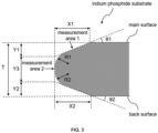
- the "surface sloping from one surface” is the surface shown in FIG. 3 below as the surface sloping from the main surface, measurement area 1, and the "surface with curvature from the point where the sloping surface ends from one surface to the point where the sloping surface ends from the other surface” is the surface shown in FIG. 3 below, which is the measurement area 2 that is the arc area of the edge part being the surface with curvature from the position where the sloping surface ends from the main surface of measurement area 1 to the position where the sloping surface ends from the back surface.
- the root mean square height Sq is preferably 0.15 ⁇ m or less
- the root mean square height Sq is preferably 0.15 ⁇ m or less. According to the configuration, the migration of residues (particles, etc.) on the substrate surface can be better prevented, and contamination of the surface of the indium phosphide substrate and yield loss during substrate production can be better controlled.
- the method for manufacturing the indium phosphide substrate starts from producing an indium phosphide ingot by a known method.
- orientation flats (OF) and index flats (IF) may be formed at predetermined locations on the outer periphery of a wafer.
- a wafer having a main surface and a back surface is then cut out from the ground indium phosphide ingot.
- both ends of the crystal of the indium phosphide ingot are cut along a predetermined crystal plane using a wire saw to cut out a plurality of wafers to have a predetermined thickness.
- both surfaces of the cut wafer are etched with a predetermined etching solution (primary etching).
- the wafer can be etched by immersing the entire wafer in the etching solution.
- an outer peripheral portion of the wafer is chamfered, and at least one surface, preferably both surfaces, of the chamfered wafer may be polished.
- the polishing step is also called a lapping step, and the wafer is polished with certain abrasives to remove irregularities on the wafer surface while maintaining the flatness of the wafer.
- the entire surface of the edge part of the wafer produced after chamfering is polished with a polishing film of #4000 grit size.
- the entire edge part of the wafer is polished with the same polishing film of #4000 grit size, so the roughness of the entire edge part of the wafer is controlled to a similar level. That is, the polishing process controls the surface roughness of the edge part of the wafer so that the maximum height Sz is 2.1 ⁇ m or less when measured with a laser microscope on the entire edge surface.
- the surface roughness of the edge part of the wafer is preferably controlled so that the root mean square height Sq is 0.15 ⁇ m or less for the entire edge surface.
- Both surfaces of the polished wafer are then etched with a predetermined etching solution (secondary etching).
- the wafer can be etched by immersing the entire wafer in the etching solution.
- the main surface of the wafer is then polished with an abrasive material for mirror polishing to finish it into a mirror surface.
- the resulting polished wafer is then washed to produce an indium phosphide wafer according to an embodiment of the present invention.
- the indium phosphide substrate of the embodiment of the present invention may be a substrate with the edge part polished with the polishing film of #4000 grit size after chamfering as described above, or the indium phosphide substrate of the embodiment of the present invention may be a substrate produced by etching, mirror polishing, cleaning, etc. after being polished with a polishing film.
- an epitaxial crystal layer By epitaxially growing a semiconductor thin film onto the main surface of the indium phosphide substrate according to the embodiment of the present invention by a known method, an epitaxial crystal layer can be formed to produce a semiconductor epitaxial wafer.
- an InAIAs buffer layer, an InGaAs channel layer, an InAIAs spacer layer and an InP electron supply layer may be epitaxially grown onto the main surface of the indium phosphide substrate to form a HEMT structure.
- a mirror-finished indium phosphide substrate is etched with an etching solution such as sulfuric acid/hydrogen peroxide solution to remove impurities such as silicon (Si) adhering to the substrate surface.
- an etching solution such as sulfuric acid/hydrogen peroxide solution to remove impurities such as silicon (Si) adhering to the substrate surface.
- the back surface of the etched indium phosphide substrate is brought into contact with the susceptor and supported, and in this state, an epitaxial film is formed on the main surface of the indium phosphide substrate by molecular beam epitaxy (MBE) or metal organic chemical vapor deposition (MOCVD).
- MBE molecular beam epitaxy
- MOCVD metal organic chemical vapor deposition
- orientation flat (OF) and index flat (IF) were formed at predetermined locations on the outer periphery of the wafer.
- a wafer having a main surface and a back surface was cut out from the ground indium phosphide ingot.
- both ends of the crystal of the indium phosphide ingot were cut along a predetermined crystal plane using a wire saw to cut out a plurality of wafers to have a predetermined thickness.
- a new wire was continuously delivered while reciprocating the wire, and the indium phosphide ingot was moved toward a wire saw.
- the wafer diameter of the wafer produced herein was 76.2 mm and the wafer thickness was 750 ⁇ m.
- the cut wafer was etched from both sides with a mixed solution of 85% by mass of an aqueous phosphoric acid solution and 30% by mass of a hydrogen peroxide solution (primary etching).
- the wafer was etched by immersing the entire wafer in the etching solution.
- an outer peripheral portion of the wafer was chamfered, and both surfaces of the chamfered wafer were polished (lapping).
- the wafer was polished with abrasives to remove irregularities on the wafer surface while maintaining the flatness of the wafer.
- the wafer after polishing with the film was etched with a mixture of 85 mass% phosphoric acid solution, 30 mass% hydrogen peroxide solution, and ultrapure water with a total etching volume of 8 to 15 ⁇ m thickness from both sides (secondary etching).
- the wafer was etched by immersing the entire wafer in the aforementioned etchant.
- the main surface of the wafer was then polished with abrasives for mirror polishing to finish it into a mirror surface, and then washed to produce an indium phosphide substrate.
- FIG. 2 is a schematic diagram of the indium phosphide substrate in plan view of the Example 1.
- FIG. 3 is a cross-sectional schematic diagram of the indium phosphide substrate according to Example 1 near the edge part.
- T 650 ⁇ m
- X1 494 ⁇ m
- X2 432 ⁇ m
- Y1 126 ⁇ m
- Y2 108 ⁇ m
- Y3 416 ⁇ m
- R1 167 ⁇ m
- R2 184 ⁇ m
- R1 and R2 are the radius of curvature of rounded edge part
- ⁇ 1 14.5 degrees
- ⁇ 2 13.9 degrees
- ⁇ 1 and ⁇ 2 are the inclination angles of edge part).
- Comparative Example 1 an indium phosphide substrate was produced in the same manner as in Example 1 above, except that after the lapping process, the edges were not polished using a polishing film and secondary etching was performed.
- the edge part to be measured on the indium phosphide substrate was divided into two areas, one located on the opposite side of the OF (A-area) and the other on the opposite side of the IF (B-area). Furthermore, as shown in FIG. 3 , (1) the surface sloping from the main surface was designated as measurement area 1, and (2) the arc area on the edge part that is a surface with curvature from the point where the sloping surface ends from main surface in measurement area 1 to the point where the sloping surface ends from the back surface is designated as measurement area 2.
- measurement area 1 in the A-area was designated as "A-area 1," measurement area 2 in the A-area as "A-area 2,” measurement area 1 in the B-area as "B-area 1" and the measurement area 2 in the B-area as "B-area 2".
- the maximum height Sz and the root mean square height Sq were measured in a total of four areas at these edge parts (each measurement area size: 258 ⁇ m ⁇ 258 ⁇ m), respectively, using an OLYMPUS OLS5000 3D measurement laser microscope.
- a cutoff filter L filter: wavelength of 20 ⁇ m to be cut was used for the measurement.
- Example 1 indium phosphide substrates were obtained with a maximum height Sz of 2.1 ⁇ m or less, as measured by laser microscopy, for each surface roughness of A-area 1 and 2 and B-area 1 and 2 at the edge part of the substrate.
- the entire edge surface of the substrate was polished with a polishing film of #4000 grit size, and the sloping area corresponding to measurement area 1 on the entire edge surface is considered to have the same surface roughness as A-area 1 and B-area 1.
- the relatively flat area (arc area) corresponding to the measurement area 2 of the edge part, such as the measurement area 2 described above is considered to have the same surface roughness as A-area 2 and B-area 2.
- the difference in the maximum height Sz and the root mean square height Sq between the area 1 and area 2 of the edge part is considered to be due to the effect of polishing the substrate surface by mirror polishing after polishing the edge part with the polishing film.
- the maximum height Sz and the root mean square height Sq are considered to be the same regardless of which area of the entire edge surface of the substrate is measured, as long as the entire edge surface is immediately after polishing with a polishing film of #4000 grit size.
- the Si concentration on the surface of the substrate in Example 1 was measured at two points by TOF-SIMS analysis.
- the Si concentration was 80.3 ( ⁇ 10 10 atoms/cm 2 ) and 115.8 ( ⁇ 10 10 atoms/cm 2 ).
- the sensitivity coefficient of the analyzer was determined based on a standard sample of known concentration, and the ionic intensity of Si was quantified by normalizing it to the In intensity.
- the indium phosphide substrate of Comparative Example 1 was not polished with a polishing film of #4000 grit size on the entire edge surface of the substrate after the chamfering and lapping processes.
- the maximum height Sz was over 2.1 ⁇ m as measured by laser microscopy for each surface roughness of the A-area 1 and A-area 2 and B-area 1 and B-area 2 at the edge part of the substrate.
Landscapes
- Chemical & Material Sciences (AREA)
- Metallurgy (AREA)
- Engineering & Computer Science (AREA)
- Crystallography & Structural Chemistry (AREA)
- Materials Engineering (AREA)
- Organic Chemistry (AREA)
- General Chemical & Material Sciences (AREA)
- Chemical Kinetics & Catalysis (AREA)
- Inorganic Chemistry (AREA)
- Crystals, And After-Treatments Of Crystals (AREA)
- Mechanical Treatment Of Semiconductor (AREA)
- Recrystallisation Techniques (AREA)
- Weting (AREA)
Applications Claiming Priority (2)
| Application Number | Priority Date | Filing Date | Title |
|---|---|---|---|
| JP2020211684A JP7166323B2 (ja) | 2020-12-21 | 2020-12-21 | リン化インジウム基板、リン化インジウム基板の製造方法及び半導体エピタキシャルウエハ |
| PCT/JP2021/037238 WO2022137727A1 (fr) | 2020-12-21 | 2021-10-07 | Substrat de phosphure d'indium, procédé de fabrication d'un substrat de phosphure d'indium et plaquette épitaxiale de semi-conducteur |
Publications (2)
| Publication Number | Publication Date |
|---|---|
| EP4207249A1 true EP4207249A1 (fr) | 2023-07-05 |
| EP4207249A4 EP4207249A4 (fr) | 2024-11-20 |
Family
ID=82158947
Family Applications (1)
| Application Number | Title | Priority Date | Filing Date |
|---|---|---|---|
| EP21909885.2A Pending EP4207249A4 (fr) | 2020-12-21 | 2021-10-07 | Substrat de phosphure d'indium, procédé de fabrication d'un substrat de phosphure d'indium et plaquette épitaxiale de semi-conducteur |
Country Status (6)
| Country | Link |
|---|---|
| US (1) | US20230378274A1 (fr) |
| EP (1) | EP4207249A4 (fr) |
| JP (2) | JP7166323B2 (fr) |
| CN (1) | CN116261772A (fr) |
| TW (1) | TWI781801B (fr) |
| WO (1) | WO2022137727A1 (fr) |
Families Citing this family (1)
| Publication number | Priority date | Publication date | Assignee | Title |
|---|---|---|---|---|
| JP7166324B2 (ja) * | 2020-12-21 | 2022-11-07 | Jx金属株式会社 | リン化インジウム基板、リン化インジウム基板の製造方法及び半導体エピタキシャルウエハ |
Family Cites Families (22)
| Publication number | Priority date | Publication date | Assignee | Title |
|---|---|---|---|---|
| JPS6117257A (ja) | 1984-07-04 | 1986-01-25 | Victor Co Of Japan Ltd | 磁気記録再生装置 |
| JP2594371B2 (ja) * | 1990-03-29 | 1997-03-26 | 信越半導体株式会社 | エピタキシャルウェーハの製造方法 |
| JP3368799B2 (ja) * | 1997-05-22 | 2003-01-20 | 住友電気工業株式会社 | Iii−v族化合物半導体ウェハおよびその製造方法 |
| JPH11204493A (ja) * | 1998-01-09 | 1999-07-30 | Komatsu Electron Metals Co Ltd | 半導体ウェハの製造方法 |
| JP3516203B2 (ja) | 1999-11-08 | 2004-04-05 | 株式会社日鉱マテリアルズ | 化合物半導体ウェハ |
| JP2008109125A (ja) | 2006-09-29 | 2008-05-08 | Sumco Techxiv株式会社 | シリコン単結晶基板及びその製造方法 |
| US8062732B2 (en) * | 2007-05-22 | 2011-11-22 | Corning Incorporated | Glass article having improved edge |
| JP4395812B2 (ja) * | 2008-02-27 | 2010-01-13 | 住友電気工業株式会社 | 窒化物半導体ウエハ−加工方法 |
| US8562849B2 (en) * | 2009-11-30 | 2013-10-22 | Corning Incorporated | Methods and apparatus for edge chamfering of semiconductor wafers using chemical mechanical polishing |
| JP5472073B2 (ja) | 2010-12-16 | 2014-04-16 | 信越半導体株式会社 | 半導体ウェーハ及びその製造方法 |
| JP2012174935A (ja) | 2011-02-22 | 2012-09-10 | Shin Etsu Handotai Co Ltd | エピタキシャルウェーハの製造方法 |
| EP4174913A1 (fr) * | 2015-02-09 | 2023-05-03 | Sumitomo Electric Industries, Ltd. | Substrat de phosphore d'indium, procédé d'inspection de substrat de phosphore d'indium et procédé de fabrication de substrat de phosphore d'indium |
| CN105161397B (zh) * | 2015-05-13 | 2019-02-05 | 北京通美晶体技术有限公司 | 一种异形半导体晶片、制备方法及晶片支承垫 |
| EP3476983A4 (fr) * | 2017-04-28 | 2020-04-01 | JX Nippon Mining & Metals Corporation | Tranche semiconductrice et procédé pour polir une tranche semiconductrice |
| EP3514266B1 (fr) * | 2017-05-26 | 2025-10-15 | Sumitomo Electric Industries, Ltd. | Substrat semi-conducteur composé du groupe iii-v et substrat semi-conducteur composé du groupe iii-v avec couche épitaxiale |
| CN109290874B (zh) * | 2017-07-25 | 2021-02-02 | 北京通美晶体技术有限公司 | 背面有橄榄形凹坑的磷化铟晶片、制法及所用腐蚀液 |
| CN109290875B (zh) * | 2017-07-25 | 2021-06-22 | 北京通美晶体技术股份有限公司 | 背面有凹坑的磷化铟晶片、制法和制备其的腐蚀液 |
| JP7125252B2 (ja) | 2017-08-30 | 2022-08-24 | 昭和電工株式会社 | SiCエピタキシャルウェハ及びその製造方法 |
| JP7017475B2 (ja) | 2018-06-19 | 2022-02-08 | 信越化学工業株式会社 | フォトマスクブランク関連基板の表面状態の評価方法 |
| US10576585B1 (en) * | 2018-12-29 | 2020-03-03 | Cree, Inc. | Laser-assisted method for parting crystalline material |
| JP7381214B2 (ja) | 2019-03-27 | 2023-11-15 | 株式会社東京精密 | ブラストユニット付き面取り装置 |
| JP7166324B2 (ja) * | 2020-12-21 | 2022-11-07 | Jx金属株式会社 | リン化インジウム基板、リン化インジウム基板の製造方法及び半導体エピタキシャルウエハ |
-
2020
- 2020-12-21 JP JP2020211684A patent/JP7166323B2/ja active Active
-
2021
- 2021-10-07 EP EP21909885.2A patent/EP4207249A4/fr active Pending
- 2021-10-07 CN CN202180067951.9A patent/CN116261772A/zh active Pending
- 2021-10-07 US US18/031,060 patent/US20230378274A1/en active Pending
- 2021-10-07 WO PCT/JP2021/037238 patent/WO2022137727A1/fr not_active Ceased
- 2021-10-25 TW TW110139521A patent/TWI781801B/zh active
-
2022
- 2022-02-08 JP JP2022018234A patent/JP2022098503A/ja not_active Withdrawn
Also Published As
| Publication number | Publication date |
|---|---|
| CN116261772A (zh) | 2023-06-13 |
| TW202226354A (zh) | 2022-07-01 |
| JP7166323B2 (ja) | 2022-11-07 |
| US20230378274A1 (en) | 2023-11-23 |
| JP2022098256A (ja) | 2022-07-01 |
| JP2022098503A (ja) | 2022-07-01 |
| EP4207249A4 (fr) | 2024-11-20 |
| WO2022137727A1 (fr) | 2022-06-30 |
| TWI781801B (zh) | 2022-10-21 |
Similar Documents
| Publication | Publication Date | Title |
|---|---|---|
| US12217967B2 (en) | Indium phosphide substrate | |
| US11894225B2 (en) | Indium phosphide substrate, semiconductor epitaxial wafer, and method for producing indium phosphide substrate | |
| EP3933891A1 (fr) | Substrat de phosphure d'indium et procédé de production de substrat de phosphure d'indium | |
| US20220199770A1 (en) | Indium phosphide substrate and method for producing indium phosphide substrate | |
| EP4215650A1 (fr) | Substrat de phosphure d'indium, procédé de fabrication de substrat de phosphure d'indium et tranche épitaxiale semi-conductrice | |
| EP3862133B1 (fr) | Procédé de fabrication de substrat de phosphure d'indium | |
| US11788203B2 (en) | Indium phosphide substrate, semiconductor epitaxial wafer, and method for producing indium phosphide substrate | |
| EP4207249A1 (fr) | Substrat de phosphure d'indium, procédé de fabrication d'un substrat de phosphure d'indium et plaquette épitaxiale de semi-conducteur | |
| TWI810847B (zh) | 磷化銦基板 | |
| US12065759B2 (en) | Indium phosphide substrate | |
| JP7713056B1 (ja) | リン化インジウム基板及び半導体エピタキシャルウエハ |
Legal Events
| Date | Code | Title | Description |
|---|---|---|---|
| STAA | Information on the status of an ep patent application or granted ep patent |
Free format text: STATUS: THE INTERNATIONAL PUBLICATION HAS BEEN MADE |
|
| PUAI | Public reference made under article 153(3) epc to a published international application that has entered the european phase |
Free format text: ORIGINAL CODE: 0009012 |
|
| STAA | Information on the status of an ep patent application or granted ep patent |
Free format text: STATUS: REQUEST FOR EXAMINATION WAS MADE |
|
| 17P | Request for examination filed |
Effective date: 20230329 |
|
| AK | Designated contracting states |
Kind code of ref document: A1 Designated state(s): AL AT BE BG CH CY CZ DE DK EE ES FI FR GB GR HR HU IE IS IT LI LT LU LV MC MK MT NL NO PL PT RO RS SE SI SK SM TR |
|
| DAV | Request for validation of the european patent (deleted) | ||
| DAX | Request for extension of the european patent (deleted) | ||
| REG | Reference to a national code |
Ref country code: DE Ref legal event code: R079 Free format text: PREVIOUS MAIN CLASS: H01L0021200000 Ipc: H01L0021020000 |
|
| A4 | Supplementary search report drawn up and despatched |
Effective date: 20241018 |
|
| RIC1 | Information provided on ipc code assigned before grant |
Ipc: C30B 29/40 20060101ALI20241014BHEP Ipc: C30B 25/18 20060101ALI20241014BHEP Ipc: H01L 21/304 20060101ALI20241014BHEP Ipc: H01L 21/20 20060101ALI20241014BHEP Ipc: H01L 21/02 20060101AFI20241014BHEP |