EP4207264A1 - Halbleiterstruktur und herstellungsverfahren dafür - Google Patents
Halbleiterstruktur und herstellungsverfahren dafür Download PDFInfo
- Publication number
- EP4207264A1 EP4207264A1 EP22782646.8A EP22782646A EP4207264A1 EP 4207264 A1 EP4207264 A1 EP 4207264A1 EP 22782646 A EP22782646 A EP 22782646A EP 4207264 A1 EP4207264 A1 EP 4207264A1
- Authority
- EP
- European Patent Office
- Prior art keywords
- conductive layer
- bit line
- semiconductor structure
- manufacturing
- line contact
- Prior art date
- Legal status (The legal status is an assumption and is not a legal conclusion. Google has not performed a legal analysis and makes no representation as to the accuracy of the status listed.)
- Pending
Links
Images


Classifications
-
- H—ELECTRICITY
- H10—SEMICONDUCTOR DEVICES; ELECTRIC SOLID-STATE DEVICES NOT OTHERWISE PROVIDED FOR
- H10B—ELECTRONIC MEMORY DEVICES
- H10B12/00—Dynamic random access memory [DRAM] devices
- H10B12/30—DRAM devices comprising one-transistor - one-capacitor [1T-1C] memory cells
- H10B12/48—Data lines or contacts therefor
- H10B12/482—Bit lines
-
- H—ELECTRICITY
- H10—SEMICONDUCTOR DEVICES; ELECTRIC SOLID-STATE DEVICES NOT OTHERWISE PROVIDED FOR
- H10B—ELECTRONIC MEMORY DEVICES
- H10B12/00—Dynamic random access memory [DRAM] devices
- H10B12/30—DRAM devices comprising one-transistor - one-capacitor [1T-1C] memory cells
- H10B12/48—Data lines or contacts therefor
- H10B12/485—Bit line contacts
-
- H—ELECTRICITY
- H10—SEMICONDUCTOR DEVICES; ELECTRIC SOLID-STATE DEVICES NOT OTHERWISE PROVIDED FOR
- H10B—ELECTRONIC MEMORY DEVICES
- H10B12/00—Dynamic random access memory [DRAM] devices
- H10B12/01—Manufacture or treatment
- H10B12/02—Manufacture or treatment for one transistor one-capacitor [1T-1C] memory cells
- H10B12/03—Making the capacitor or connections thereto
-
- H—ELECTRICITY
- H10—SEMICONDUCTOR DEVICES; ELECTRIC SOLID-STATE DEVICES NOT OTHERWISE PROVIDED FOR
- H10B—ELECTRONIC MEMORY DEVICES
- H10B12/00—Dynamic random access memory [DRAM] devices
- H10B12/01—Manufacture or treatment
- H10B12/09—Manufacture or treatment with simultaneous manufacture of the peripheral circuit region and memory cells
-
- H—ELECTRICITY
- H10—SEMICONDUCTOR DEVICES; ELECTRIC SOLID-STATE DEVICES NOT OTHERWISE PROVIDED FOR
- H10B—ELECTRONIC MEMORY DEVICES
- H10B12/00—Dynamic random access memory [DRAM] devices
- H10B12/30—DRAM devices comprising one-transistor - one-capacitor [1T-1C] memory cells
- H10B12/31—DRAM devices comprising one-transistor - one-capacitor [1T-1C] memory cells having a storage electrode stacked over the transistor
- H10B12/315—DRAM devices comprising one-transistor - one-capacitor [1T-1C] memory cells having a storage electrode stacked over the transistor with the capacitor higher than a bit line
Definitions
- the present disclosure relates to the technical field of semiconductors, and in particular to a semiconductor structure and a manufacturing method thereof.
- DRAM dynamic random access memory
- a DRAM generally includes a plurality of memory cells, each of which includes a transistor and a capacitor.
- the transistor includes a gate electrically connected to a word line, a source electrically connected to a bit line through a bit line contact structure, and a drain electrically connected to a capacitor through a capacitor contact.
- a word line voltage on the word line can control the on or off of the transistor, so as to read data information stored in the capacitor or write data information into the capacitor.
- bit line contact structure during forming of the bit line contact structure, a gap easily appears in the bit line contact structure, which may cause an electric connection between the capacitor contact structure and the bit line, thus reducing the yield of the semiconductor structure.
- an embodiment of the present disclosure provides a manufacturing method of a semiconductor structure, including:
- the concentration of the doped impurities in the second conductive layer is 1.5 to 3 times the concentration of the doped impurities in the first conductive layer.
- the forming a first conductive layer in each of the bit line contact regions includes:
- the longitudinal section of the contact hole is in a shape of trapezoid with a large top and a small bottom.
- the longitudinal section of the contact hole is V-shaped.
- an angle between a sidewall of the contact hole and the direction perpendicular to the substrate ranges from 10° to 20°.
- a thickness of the first conductive layer ranges from 0 nm to 6 nm in a first direction.
- a thickness of the first conductive layer on a bottom wall of the bit line contact region ranges from 5 nm to 8 nm.
- a thickness of the first initial conductive layer ranges from 5 nm to 18 nm in a first direction.
- a thickness of the first initial conductive layer on a bottom wall of the bit line contact region ranges from 10 nm to 18 nm.
- materials of the first conductive layer and the second conductive layer include polysilicon, and the doped impurities are phosphorus ions.
- the manufacturing method before the forming a first conductive layer in each of the bit line contact regions, the manufacturing method further includes: forming a protective layer on a sidewall of each of the bit line contact regions.
- a thickness of the protective layer ranges from 3 nm to 6 nm, and a material of the protective layer includes polysilicon.
- the etching gas includes chlorine, and an etching temperature ranges from 250°C to 320°C.
- an embodiment of the present disclosure provides a semiconductor structure, which is manufactured using the manufacturing method of a semiconductor structure in the foregoing embodiment.
- 10 substrate; 11: active region; 12: isolation structure; 13: bit line contact region; 20: conductive layer; 21: first conductive layer; 22: second conductive layer; 23: first initial conductive layer; 24: intermediate hole; 25: contact hole; 30: mask layer; 40: protective layer.
- bit line structures and isolation side walls covering the bit line structures are formed first.
- the bit line structure includes a bit line contact structure and a bit line that are sequentially stacked.
- a capacitor contact structure is formed between adjacent isolation side walls.
- the capacitor contact structure is configured to connect a capacitor and an active region of the substrate, to implement storage of data.
- a bit line contact region is first formed in the substrate 10, and then a conductive layer 20 is formed in the bit line contact region.
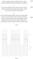
- a gap will be formed in the conductive layer 20.
- the conductive layer 20 is etched to form the bit line contact structure, the gap will be exposed, causing some regions of the bit line contact structure to be discontinuous, and during forming of the isolation side wall, an insulating material for forming the isolation side wall will be filled into the gap. Consequently, the isolation side wall is broken at the gap, and fails to cover the bit line completely.
- an electric connection easily occurs between the capacitor contact structure and the bit line structure, reducing the yield of the semiconductor structure.
- a first conductive layer and a second conductive layer are formed through two deposition processes separately, and a concentration of doped impurities in the first conductive layer is lower than a concentration of doped impurities in the second conductive layer. Because a lower concentration of doped impurities corresponds to a higher filling capability, no gap is formed during forming of the first conductive layer.
- a contact hole is defined in a bit line contact region of the first conductive layer, and the contact hole has a low depth-to-width ratio. In this way, during forming of the second conductive layer, no gap is formed in the second conductive layer, thereby avoiding forming a gap in the conductive layer. Therefore, when a bit line structure and an isolation side wall are formed subsequently, the isolation side wall will not be damaged, thereby avoiding the electric connection between a capacitor contact structure and a bit line, and improving the yield of the semiconductor structure.
- FIG. 3 is a flowchart of a manufacturing method of a semiconductor structure according to an embodiment of the present disclosure.
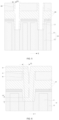
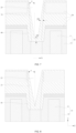
- FIG. 4 to FIG. 10 are schematic diagrams of various stages in a manufacturing method of a semiconductor structure. The manufacturing method of a semiconductor structure will be described in detail below with reference to FIG. 4 to FIG. 10 .
- the semiconductor structure is not limited in this embodiment.
- the semiconductor structure is described below by taking a dynamic random access memory (DRAM) as an example, but this embodiment is not limited to this, and the semiconductor structure in this embodiment may also be other structure.
- DRAM dynamic random access memory
- an embodiment of the present disclosure provides a manufacturing method of a semiconductor structure, including the following steps: Step S100: Provide a substrate, where a plurality of bit line contact regions arranged at intervals are provided in the substrate.
- a substrate 10 serves as a support member of the DRAM and is used to support other components thereon.
- the substrate 10 may be made of a semiconductor material.
- the semiconductor material may be one or more of a group consisting of silicon, germanium, a silicon-germanium compound, and a silicon-carbon compound.
- the substrate 10 is provided with a plurality of active regions 11 and isolation structures 12 for isolating the active regions 11.
- the plurality of active regions 11 may be arranged at intervals.
- the active region 11 is used for disposing a semiconductor device, such as a transistor and a capacitor.
- a manufacturing process of the isolation structures 12 generally includes: patterning the substrate 10 to form isolation trenches in the substrate 10, then depositing silicon oxide in the isolation trenches by using a deposition process, to form the isolation structures 12.
- the isolation structures 12 are used for insulating the active regions 11 from each other.
- the substrate 10 is provided with a plurality of bit line contact regions 13.
- the plurality of bit line contact regions 13 may be arranged at intervals in the substrate 10.
- a patterned mask layer 30 may be formed on the substrate 10. Then, with the mask layer 30 as a mask, the substrate 10 is removed by a certain thickness by using an etching gas or an etching liquid, to form the bit line contact regions 13 in the substrate 10.
- a photoetching layer with a specific thickness may be coated on the mask layer 30, and then a mask pattern is formed on the photoetching layer through exposure, etching, and development. Next, the mask layer 30 not covered by the mask pattern is removed by using an etching liquid or an etching gas, to form a pattern in the mask layer 30.
- the mask layer 30 may be a single film layer or a composite film layer.
- the mask layer 30 may include a silicon nitride layer, a polysilicon layer, and a silicon oxide layer that are sequentially stacked.
- the silicon nitride layer is disposed on the substrate 10.
- the mask layer 30 is a composite film layer, so that the pattern is first transferred to the silicon oxide layer, and then transferred to the polysilicon layer, the silicon nitride layer, and the substrate 10 in sequence in a pattern transfer process, thereby improving the accuracy of the pattern transfer process and ensuring the accuracy of the pattern of the bit line contact region 13.
- a protective layer 40 may be formed in the bit line contact region 13, or the conductive layer 20 may be formed directly.
- forming the protective layer 40 in the bit line contact region 13 is taken as an example for illustration.
- the protective layer 40 is formed on a sidewall of the bit line contact region 13.
- the protective layer 40 is used for protecting the isolation structure 12 exposed in the bit line contact region 13, to prevent damage on the isolation structure 12 when the bit line contact region 13 is cleaned subsequently.
- a material of the protective layer 40 includes polysilicon.
- a thickness of the protective layer 40 ranges from 3 nm to 6 nm. As shown in FIG. 5 , the protective layer 40 has a certain thickness D1 in direction X, where the thickness D1 ranges from 3 nm to 6 nm.
- the thickness of the protective layer 40 is less than 3 nm, the protective layer 40 is excessively thin. As a result, the isolation structure 12 will still be damaged when the bit line contact region 13 is subsequently cleaned. If the thickness of the protective layer 40 is greater than 6 nm, an area of a region defined by the protective layer 40 is excessively small, which increases the depth-to-width ratio of the region. As a result, the subsequently formed bit line contact structure will still have a gap.
- the thickness of the protective layer 40 is limited in this embodiment, which not only protects the isolation structure 12 but also prevents a gap in the bit line contact structure, thereby avoiding an electric connection between the capacitor contact structure and the bit line structure and improving the yield of the semiconductor structure.
- Step S200 Form a first conductive layer in each of the bit line contact regions, where the first conductive layer defines a contact hole in each of the bit line contact regions.
- the first conductive layer 21 is formed through a deposition process.
- the deposition process may include at least one of a physical vapor deposition process, a chemical vapor deposition process, and an atomic layer deposition process.
- Step S300 Form a second conductive layer in each of the contact holes, where the second conductive layer and the first conductive layer form a conductive layer, a concentration of doped impurities in the second conductive layer is higher than a concentration of doped impurities in the first conductive layer, and the structure is as shown in FIG. 9 and FIG. 10 .
- the second conductive layer 22 may also be formed through a deposition process.
- the deposition process may include at least one of a physical vapor deposition process, a chemical vapor deposition process, and an atomic layer deposition process.
- materials of the first conductive layer 21 and the second conductive layer 22 are polysilicon, and the doped impurities are phosphorus ions.
- the concentration of the doped impurities in the second conductive layer 22 is 1.5 to 3 times the concentration of the doped impurities in the first conductive layer 21.
- the concentration of the doped impurities in the first conductive layer 21 is 1E20 to 10E20. That is, the concentration of the doped impurities in the first conductive layer 21 is 1*10 20 to 10*10 20 .
- the concentration of the doped impurities in the second conductive layer 22 is 15E20 to 30E20. That is, the concentration of the doped impurities in the second conductive layer 22 is 15*10 20 to 30*10 20 .
- the conductive layer 20 is formed through two deposition processes. That is, the first deposition process is used for forming the first conductive layer 21, and the second deposition process is used for forming the second conductive layer 22, where a concentration of doped impurities in the first conductive layer 21 is lower than a concentration of doped impurities in the second conductive layer 22. Because a lower concentration of doped impurities corresponds to a higher filling capability, no gap is formed during forming of the first conductive layer 21.
- the contact hole 25 is defined in the bit line contact region 13 of the first conductive layer 21, and the contact hole 25 has a low depth-to-width ratio.
- the high concentration of the doped impurities in the second conductive layer 22 can improve the conductivity of the second conductive layer 22, thereby improving the conductivity of the conductive layer 20 and the performance of the semiconductor structure.
- the process of forming a first conductive layer 21 in each of the bit line contact regions 13 may be implemented in the following manner.
- a first initial conductive layer 23 is formed in each of the bit line contact regions 13 by using a deposition process.
- the first initial conductive layer 23 extends to the outside of the bit line contact region 13 and covers the mask layer 30.
- the first initial conductive layer 23 defines an intermediate hole 24 in each of the bit line contact regions 13.
- the deposition process may include at least one of a physical vapor deposition process, a chemical vapor deposition process, and an atomic layer deposition process.
- a thickness of the first initial conductive layer 23 ranges from 5 nm to 18 nm.
- the thickness of the first initial conductive layer 23 is D2 as shown in FIG. 6 . If the thickness of the first initial conductive layer 23 is less than 5 nm, it makes it difficult to form the first conductive layer 21 subsequently. If the thickness of the first initial conductive layer 23 is greater than 18 nm, the first initial conductive layer 23 is excessively thick, which makes it difficult to form the intermediate hole 24 and subsequently remove the first initial conductive layer 23. Therefore, in this embodiment, the thickness of the first initial conductive layer 23 is limited in the range of 5 nm to 18 nm, which not only facilitates forming of the first conductive layer 21 but also reduces the manufacturing difficulty of the first conductive layer 21.
- the first direction may be direction X in FIG. 6 .
- a thickness of the first initial conductive layer 23 on a bottom wall of the bit line contact region 13 ranges from 10 nm to 18 nm.
- the thickness of the first initial conductive layer 23 on the bottom wall of the bit line contact region 13 is D3 as shown in FIG. 6 .
- the subsequently formed first conductive layer 21 is excessively thin in a direction perpendicular to the substrate 10, and thus the contact hole 25 is still very deep, which may cause a gap in the subsequently formed second conductive layer 22.
- the thickness of the first initial conductive layer 23 on the bottom wall of the bit line contact region 13 is greater than 18 nm, the depth of the subsequently formed contact hole 25 is reduced, which leads to low conductivity of the subsequently formed second conductive layer 22, thus reducing the conductivity of the conductive layer 20.
- the thickness of the first initial conductive layer 23 on the bottom wall of the bit line contact region 13 is limited in a range of 10 nm to 18 nm, which not only avoids forming a gap in the second conductive layer 22 but also improves the conductivity of the conductive layer 20, thereby improving the performance of the semiconductor structure.
- an etching gas is introduced into the intermediate hole 24.
- the etching gas can remove a part of the first initial conductive layer 23, the retained first initial conductive layer 23 forms the first conductive layer 21, and the first conductive layer 21 defines the contact hole 25 in the bit line contact region.
- the etching gas includes chlorine, and an etching temperature ranges from 250°C to 320°C.
- An etching temperature lower than 250°C will reduce an etching rate and an etching time, thus increasing the production cost.
- An etching temperature higher than 320°C easily causes over-etching of the first initial conductive layer 23 and reduces the thickness of the first conductive layer 21, and thus the contact hole 25 still has a high depth-to-width ratio. Therefore, in this embodiment, the etching temperature is limited, which not only reduces the production cost but also reduces the depth-to-width ratio of the contact hole 25, thereby avoiding forming a gap in the bit line contact structure.
- the contact hole 25 may be in various shapes.
- the longitudinal section of the contact hole 25 is in a shape of a trapezoid with a large top and a small bottom, where the structure is as shown in FIG. 7 .
- the longitudinal section of the contact hole 25 is V-shaped, where the structure is as shown in FIG. 8 .
- the shape of the contact hole 25 is limited, which can facilitate subsequent deposition of the second conductive layer 22 and avoid forming a gap in the second conductive layer 22.
- an angle between a sidewall of the contact hole 25 and the direction perpendicular to the substrate 10 ranges from 10° to 20°; an angle between the sidewall of the contact hole 25 and direction Y is ⁇ in FIG. 7 and FIG. 8 .
- the contact hole 25 is not deep enough, which causes the subsequently formed second conductive layer 22 to be excessively thin and reduces the conductivity of the second conductive layer 22, thus reducing the conductivity of the conductive layer 20 and the performance of the semiconductor structure.
- the angle between the sidewall of the contact hole 25 and the direction perpendicular to the substrate 10 is limited in this embodiment, which not only avoids forming a gap in the second conductive layer 22 but also increases the conductivity of the conductive layer 20.
- a thickness of the first conductive layer 21 ranges from 0 nm to 6 nm.
- the thickness of the first conductive layer 21 is D4, and the thickness D4 of the first conductive layer 21 ranges from 0 nm to 6 nm.
- the thickness of the first conductive layer 21 may be a constant value, that is, the thickness of the first conductive layer 21 remains unchanged at each position in the direction perpendicular to the substrate 10. In the direction perpendicular to the substrate 10, the thickness of the first conductive layer 21 may be change gradually. For example, as shown in FIG.
- the thickness of the first conductive layer 21 at the top of the contact hole 25 may range from 0 nm to 3 nm, and the thickness of the first conductive layer 21 at the bottom of the contact hole 25 may range from 3 nm to 6 nm.
- the thickness of the first conductive layer 21 is limited in this embodiment, which not only avoids forming a gap in the first conductive layer 21 but also ensures the conductivity of the conductive layer 20, thereby improving the performance of the semiconductor structure.
- a thickness of the first conductive layer 21 on a bottom wall of the bit line contact region 13 ranges from 5 nm to 8 nm.
- a thickness D5 of the first conductive layer 21 ranges from 5 nm to 8 nm. If the thickness D5 of the first conductive layer 21 is less than 5 nm, the contact hole 25 will still have a high depth-to-width ratio. As a result, during forming of the second conductive layer 22, a gap is easily formed in the second conductive layer 22, thus leasing to an electric connection between the subsequently formed capacitor contact structure and the bit line structure and reducing the yield of the semiconductor structure.
- the contact hole 25 is not deep enough, which may cause the formed second conductive layer 22 to be excessively thin and reduce the conductivity of the second conductive layer 22, thus reducing the conductivity of the conductive layer 20 and the performance of the semiconductor structure.
- the thickness of the first conductive layer 21 in the direction perpendicular to the substrate 10 is limited in this embodiment, which not only avoids an electric connection between the subsequently formed capacitor contact structure and the bit line structure and improves the yield of the semiconductor structure, but also ensures the conductivity of the conductive layer 20 and improves the performance of the semiconductor structure.
- an embodiment of the present disclosure provides a semiconductor structure, which is manufactured using the manufacturing method of a semiconductor structure in the foregoing embodiment. Therefore, in this embodiment, a bit line contact structure in the semiconductor structure includes a first conductive layer 21 and a second conductive layer 22 that are sequentially stacked, and the first conductive layer 21 and the second conductive layer 22 are dense structures without any gap. In this way, during subsequent forming of a bit line and an isolation side wall, the isolation side wall will not be damaged, thus avoiding an electric connection between a capacitor contact structure and a bit line structure, and improving the yield of the semiconductor structure.
- the concentration of doped impurities in the second conductive layer 22 is relatively high, which not only avoids the gap in the second conductive layer 22 but also improves the conductivity of the second conductive layer 22, thereby improving the conductivity of the bit line contact structure and the performance of the semiconductor structure.
Landscapes
- Engineering & Computer Science (AREA)
- Manufacturing & Machinery (AREA)
- Internal Circuitry In Semiconductor Integrated Circuit Devices (AREA)
Applications Claiming Priority (2)
| Application Number | Priority Date | Filing Date | Title |
|---|---|---|---|
| CN202111192543.4A CN115988869B (zh) | 2021-10-13 | 2021-10-13 | 半导体结构及其制备方法 |
| PCT/CN2022/071263 WO2023060796A1 (zh) | 2021-10-13 | 2022-01-11 | 半导体结构及其制备方法 |
Publications (2)
| Publication Number | Publication Date |
|---|---|
| EP4207264A1 true EP4207264A1 (de) | 2023-07-05 |
| EP4207264A4 EP4207264A4 (de) | 2023-11-29 |
Family
ID=85796799
Family Applications (1)
| Application Number | Title | Priority Date | Filing Date |
|---|---|---|---|
| EP22782646.8A Pending EP4207264A4 (de) | 2021-10-13 | 2022-01-11 | Halbleiterstruktur und herstellungsverfahren dafür |
Country Status (2)
| Country | Link |
|---|---|
| US (1) | US12150296B2 (de) |
| EP (1) | EP4207264A4 (de) |
Families Citing this family (1)
| Publication number | Priority date | Publication date | Assignee | Title |
|---|---|---|---|---|
| CN119028903B (zh) * | 2023-05-16 | 2025-11-14 | 长鑫存储技术有限公司 | 半导体结构的制作方法 |
Family Cites Families (10)
| Publication number | Priority date | Publication date | Assignee | Title |
|---|---|---|---|---|
| KR19990040443A (ko) | 1997-11-18 | 1999-06-05 | 윤종용 | 미세한 선폭과 고 종횡비를 갖는 영역에 절연막을 채우는 방법 |
| KR100834739B1 (ko) * | 2006-09-14 | 2008-06-05 | 삼성전자주식회사 | 반도체 소자 및 그 제조 방법 |
| CN103855002A (zh) | 2012-11-28 | 2014-06-11 | 上海华虹宏力半导体制造有限公司 | 一种超级结深沟槽填充工艺方法 |
| CN108962894B (zh) | 2018-06-22 | 2024-01-16 | 长鑫存储技术有限公司 | 一种填充沟槽形成触点的方法 |
| US10546863B1 (en) * | 2018-08-02 | 2020-01-28 | Micron Technology, Inc. | Method for fabricating bit line contact |
| KR20200046202A (ko) * | 2018-10-23 | 2020-05-07 | 삼성전자주식회사 | 반도체 장치 |
| CN112530946B (zh) * | 2019-09-18 | 2022-12-16 | 长鑫存储技术有限公司 | 半导体结构及其制作方法 |
| CN111430226B (zh) | 2020-04-10 | 2023-04-07 | 中国科学院微电子研究所 | 一种多晶硅的沉积方法及其应用 |
| CN113314469B (zh) | 2021-05-27 | 2022-03-18 | 长鑫存储技术有限公司 | 位线接触结构及其形成方法、半导体结构和半导体器件 |
| CN113658918B (zh) | 2021-08-17 | 2023-05-23 | 福建省晋华集成电路有限公司 | 半导体器件的制备方法及半导体器件 |
-
2022
- 2022-01-11 EP EP22782646.8A patent/EP4207264A4/de active Pending
- 2022-06-07 US US17/805,738 patent/US12150296B2/en active Active
Also Published As
| Publication number | Publication date |
|---|---|
| US12150296B2 (en) | 2024-11-19 |
| US20230114038A1 (en) | 2023-04-13 |
| EP4207264A4 (de) | 2023-11-29 |
Similar Documents
| Publication | Publication Date | Title |
|---|---|---|
| KR101115180B1 (ko) | 반도체 구조물들 및 반도체 구조물들의 형성 방법들 | |
| US5284787A (en) | Method of making a semiconductor memory device having improved electrical characteristics | |
| US20240008263A1 (en) | Semiconductor structure and method for manufacturing same | |
| CN114530419A (zh) | 存储器的形成方法及存储器 | |
| CN114864501A (zh) | 三维存储器及其形成方法 | |
| US12557266B2 (en) | Fabrication method of a lateral 3D memory device | |
| CN117222223A (zh) | 半导体结构及其形成方法 | |
| CN115988869B (zh) | 半导体结构及其制备方法 | |
| US20230411412A1 (en) | Semiconductor structure and forming method thereof | |
| US20240064962A1 (en) | Doped dielectric material | |
| EP4207264A1 (de) | Halbleiterstruktur und herstellungsverfahren dafür | |
| US6174781B1 (en) | Dual damascene process for capacitance fabrication of DRAM | |
| JPH08213568A (ja) | 半導体メモリ装置及びその製造方法 | |
| CN117337024A (zh) | 半导体结构及其形成方法 | |
| US7682897B2 (en) | DRAM fabrication method using oxidation spacers on pillar dielectric sidewalls | |
| US11856756B2 (en) | Semiconductor structure and manufacturing method thereof | |
| US12550312B2 (en) | Three-dimensional memory and formation method thereof | |
| US12225718B2 (en) | Semiconductor structure and method for forming semiconductor structure | |
| US20230345706A1 (en) | Semiconductor structure, method for manufacturing same, and memory | |
| US6586300B1 (en) | Spacer assisted trench top isolation for vertical DRAM's | |
| WO2023029392A1 (zh) | 半导体结构及其形成方法 | |
| US12464708B2 (en) | Semiconductor structure and method for fabricating same | |
| CN117529103B (zh) | 半导体结构及其形成方法 | |
| US12426234B2 (en) | Semiconductor structure for DRAM having a pillar lower electrode and formation method thereof | |
| US12575087B2 (en) | Semiconductor structure and manufacturing method thereof |
Legal Events
| Date | Code | Title | Description |
|---|---|---|---|
| STAA | Information on the status of an ep patent application or granted ep patent |
Free format text: STATUS: UNKNOWN |
|
| STAA | Information on the status of an ep patent application or granted ep patent |
Free format text: STATUS: THE INTERNATIONAL PUBLICATION HAS BEEN MADE |
|
| PUAI | Public reference made under article 153(3) epc to a published international application that has entered the european phase |
Free format text: ORIGINAL CODE: 0009012 |
|
| STAA | Information on the status of an ep patent application or granted ep patent |
Free format text: STATUS: REQUEST FOR EXAMINATION WAS MADE |
|
| 17P | Request for examination filed |
Effective date: 20221011 |
|
| AK | Designated contracting states |
Kind code of ref document: A1 Designated state(s): AL AT BE BG CH CY CZ DE DK EE ES FI FR GB GR HR HU IE IS IT LI LT LU LV MC MK MT NL NO PL PT RO RS SE SI SK SM TR |
|
| REG | Reference to a national code |
Ref country code: DE Ref legal event code: R079 Free format text: PREVIOUS MAIN CLASS: H01L0021824200 Ipc: H10B0012000000 |
|
| A4 | Supplementary search report drawn up and despatched |
Effective date: 20231030 |
|
| RIC1 | Information provided on ipc code assigned before grant |
Ipc: H10B 12/00 20230101AFI20231024BHEP |
|
| RIN1 | Information on inventor provided before grant (corrected) |
Inventor name: YAN, XUN |
|
| DAV | Request for validation of the european patent (deleted) | ||
| DAX | Request for extension of the european patent (deleted) |