EP4207643B1 - Procédé, dispositif et système de communication, et support de stockage lisible par ordinateur - Google Patents
Procédé, dispositif et système de communication, et support de stockage lisible par ordinateur Download PDFInfo
- Publication number
- EP4207643B1 EP4207643B1 EP21871296.6A EP21871296A EP4207643B1 EP 4207643 B1 EP4207643 B1 EP 4207643B1 EP 21871296 A EP21871296 A EP 21871296A EP 4207643 B1 EP4207643 B1 EP 4207643B1
- Authority
- EP
- European Patent Office
- Prior art keywords
- data
- bit
- target
- identification
- data packet
- Prior art date
- Legal status (The legal status is an assumption and is not a legal conclusion. Google has not performed a legal analysis and makes no representation as to the accuracy of the status listed.)
- Active
Links
Images




Classifications
-
- H—ELECTRICITY
- H04—ELECTRIC COMMUNICATION TECHNIQUE
- H04L—TRANSMISSION OF DIGITAL INFORMATION, e.g. TELEGRAPHIC COMMUNICATION
- H04L69/00—Network arrangements, protocols or services independent of the application payload and not provided for in the other groups of this subclass
- H04L69/22—Parsing or analysis of headers
-
- G—PHYSICS
- G06—COMPUTING OR CALCULATING; COUNTING
- G06F—ELECTRIC DIGITAL DATA PROCESSING
- G06F13/00—Interconnection of, or transfer of information or other signals between, memories, input/output devices or central processing units
- G06F13/38—Information transfer, e.g. on bus
- G06F13/42—Bus transfer protocol, e.g. handshake; Synchronisation
- G06F13/4265—Bus transfer protocol, e.g. handshake; Synchronisation on a point to point bus
-
- G—PHYSICS
- G06—COMPUTING OR CALCULATING; COUNTING
- G06F—ELECTRIC DIGITAL DATA PROCESSING
- G06F13/00—Interconnection of, or transfer of information or other signals between, memories, input/output devices or central processing units
- G06F13/38—Information transfer, e.g. on bus
- G06F13/42—Bus transfer protocol, e.g. handshake; Synchronisation
- G06F13/4282—Bus transfer protocol, e.g. handshake; Synchronisation on a serial bus, e.g. I2C bus, SPI bus
-
- H—ELECTRICITY
- H04—ELECTRIC COMMUNICATION TECHNIQUE
- H04L—TRANSMISSION OF DIGITAL INFORMATION, e.g. TELEGRAPHIC COMMUNICATION
- H04L67/00—Network arrangements or protocols for supporting network services or applications
- H04L67/01—Protocols
- H04L67/12—Protocols specially adapted for proprietary or special-purpose networking environments, e.g. medical networks, sensor networks, networks in vehicles or remote metering networks
-
- H—ELECTRICITY
- H04—ELECTRIC COMMUNICATION TECHNIQUE
- H04L—TRANSMISSION OF DIGITAL INFORMATION, e.g. TELEGRAPHIC COMMUNICATION
- H04L69/00—Network arrangements, protocols or services independent of the application payload and not provided for in the other groups of this subclass
- H04L69/06—Notations for structuring of protocol data, e.g. abstract syntax notation one [ASN.1]
-
- H—ELECTRICITY
- H04—ELECTRIC COMMUNICATION TECHNIQUE
- H04L—TRANSMISSION OF DIGITAL INFORMATION, e.g. TELEGRAPHIC COMMUNICATION
- H04L69/00—Network arrangements, protocols or services independent of the application payload and not provided for in the other groups of this subclass
- H04L69/18—Multiprotocol handlers, e.g. single devices capable of handling multiple protocols
Definitions
- This disclosure relates to the field of communication technologies, and the invention in particular relates to a communication method and system, a communication device, and a computer-readable storage medium.
- serial universal input and output serial universal input and output
- I/O input/output
- WO 2005/057881 A1 discloses: a data interface for transferring digital data between a host and a client over a communication path using packet structures linked together to form a communication protocol for communicating a pre-selected set of digital control and presentation data.
- the signal protocol is used by link controllers configured to generate, transmit, and receive packets forming the communications protocol, and to form digital data into one or more types of data packets, with at least one residing in the host device and being coupled to the client through the communications path.
- the interface provides a cost-effective, low power, bi-directional, highspeed data transfer mechanism over a short-range "serial" type data link, which lends itself to implementation with miniature connectors and thin flexible cables which are especially useful in connecting display elements such as wearable micro-displays to portable computers and wireless communication devices.
- DE 4304305 A1 addresses the technical problem of the susceptibility of conventional data communication devices in multiplex transmission mode to pulse width distortions and deviations caused by factors like stray capacitance, interference with communication lines, and changes in the DC component of the communication signals. These effects can lead to incorrect decoding of the transmitted data, which is particularly problematic when the changes in pulse width are significant enough to make the "1" and "0" data bits indistinguishable.
- a data communication device that ensures reliable decoding of communication data despite variations in pulse width by detecting and measuring the time intervals of rising and/or falling edges within communication signals.
- EP 1 553 738 A1 aims at increasing the performance of transmission and storage methods in the field of data streaming.
- a method and an apparatus for generating data packets are suggested wherein a data packet to be filled having a first end near its start address and a second end near its end address as well as payload data (Data 1 to Data 5) to be filled in the data packet are provided.
- the data packet is filled with the payload data beginning at the second end of the data packet.
- the start position of each payload entity (Data 1 to Data 5) does not depend on the size of the header anymore but only on the size of its predecessors, each payload entity can be stored in the packet buffer immediately without intermediate use of an temporary buffer.
- the object of the present invention is to provide a communication method and system, a device, and a computer-readable storage medium Such that when the communication method is used for communication, hardware resources of a communication device can be effectively saved, thereby reducing hardware costs.
- a communication manner between devices includes serial communication and parallel communication.
- serial communication has advantages such as a simple structure, fewer signal cables, easy to implement long-distance signal transmission, and low costs. Therefore, in a current server product, communication between different chips (for example, a complex programming logic device (complex programming logic device, CPLD)) in a server is usually implemented in a serial communication manner, for example, the SGPIO protocol.
- FIG. 1 shows a topology diagram of the SGPIO protocol.
- a chip A is a master (master) device
- a chip B is a slave (slave) device.
- the chip A and the chip B communicate with each other by using the SGPIO protocol (that is, a group of SGPIO buses).
- a group of SGPIO buses may specifically include four signal cables, which are respectively a clock cable, a signal loading cable, a data output cable, and a data input cable.
- the clock cable is configured to transmit a clock signal (CLK) sent from the chip A to the chip B, so that the chip A and the chip B can implement synchronous communication.
- the signal loading cable is configured to transmit a data loading and synchronization signal (Load) sent from the chip A to the chip B, where the data loading and synchronization signal is used to indicate that a frame of new data is to be transmitted.
- the data output cable is configured to transmit a data signal (DataOut) sent from the chip A to the chip B.
- the data input cable is configured to transmit the data signal (DataIn) sent from the chip B to the chip A.
- the chip A is connected to one side of the four signal cables through four I/O ports (for example, a port 1 to a port 4), and the chip B is connected to the other side of the four signal cables through four I/O ports (for example, a port 5 to a port 8).
- the four I/O ports of the chip A and the four I/O ports of the chip B need to be occupied to implement communication between the chip A and the chip B.
- a quantity of signal cables included in the group of SGPIO buses may be correspondingly reduced to 3, that is, a clock cable, a signal loading cable, and a data output cable.
- three I/O ports of the chip A and three I/O ports of the chip B still need to be occupied.
- the SGPIO bus occupies a large quantity of hardware resources (I/O resources). Therefore, the SGPIO protocol is not applicable to an application scenario in which I/O ports of the chip A and/or the chip B are insufficient.
- FIG. 1 shows a schematic principle diagram of identifying whether a cable is correctly connected by using a PWM signal.
- PWM pulse width modulation
- a port 1 of a chip A sends a PWM signal (PWM 1) to a port 5 of a chip B through a clock cable
- a port 2 of the chip A sends a PWM signal (PWM 2) to a port 6 of the chip B through a signal loading cable
- a port 3 of the chip A sends a PWM signal (PWM 3) to a port 7 of the chip B through a data output cable
- a port 4 of the chip A sends a PWM signal (PWM 4) to a port 8 of the chip B through a data input cable.
- a duty cycle of the PWM 1 is 3/7
- a duty cycle of the PWM 2 is 2/3
- a duty cycle of the PWM 3 is 1
- a duty cycle of the PWM 4 is 3/2. Therefore, the chip B may determine, based on a duty cycle of a PWM signal sent by the chip A, whether a signal cable is correctly connected. Specifically, the clock cable is used as an example. After receiving the PWM 1 sent by the port 1 of the chip A, the port 5 of the chip B detects that the duty cycle of the PWM 1 is 3/7, and then determines whether the duty cycle of the PWM 1 is the same as a preset duty cycle.
- the chip B determines that the clock cable is correctly connected, that is, the clock cable is a cable connected between the port 1 of the chip A and the port 5 of the chip B. It should be understood that a manner in which the chip B determines whether the signal loading cable, the data output cable, and the data input cable are correctly connected is similar to the foregoing manner in which the chip B determines whether the clock cable is correctly connected, and details are not described herein again.
- the chip B may not only communicate with the chip A, but also may be connected to a plurality of other chips or devices. In this case, a large quantity of cables are inserted into the chip B (for example, the port 5), and the port 5 also receives a large quantity of PWM signals.
- a plurality of approximately equal duty cycles may be obtained by calculating duty cycles of these PWM signals.
- the port 5 cannot accurately determine whether the cables corresponding to the PWM signals with approximately equal duty cycles are correctly connected.
- the port 5 of the chip B receives two PWM signals whose duty cycles are approximately 3/7, where one is sent by the port 1 of the chip A, and the other is sent by a port 9 of a chip C.
- the chip B cannot determine whether the other end of the clock cable is connected to the port 1 of the chip A or connected to the port 9 of the chip C, and therefore cannot determine whether the clock cable is correctly connected.
- FIG. 3 shows a topology diagram of the single-line asynchronous serial communication protocol according to this embodiment of this application. It can be learned from FIG. 3 that the protocol can implement data communication between a first device and a second device through only one signal cable (target signal cable). Therefore, when data communication is performed by using the single-wire asynchronous serial communication protocol provided in this embodiment of this application, hardware resources can be effectively saved. In addition, when cable information is transmitted by using the single-wire asynchronous serial communication protocol provided in this embodiment of this application, it can be further effectively determined whether a cable (including the target signal cable) between the first device and the second device is correctly connected. To better understand the single-line asynchronous serial communication protocol provided in this embodiment of this application, the following describes the protocol in detail by using data communication between the first device and the second device in FIG. 3 as an example.
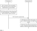
- FIG. 4 shows a schematic flowchart of a communication method according to an embodiment of this application.
- the communication method provided in this embodiment of this application includes but is not limited to the following steps.
- S101 A first device constructs to-be-sent multi-bit target data into at least one target data packet based on a preset format.
- the to-be-sent multi-bit target data is binary data, and specifically includes binary data 0 and binary data 1.
- Each target data packet in the at least one target data packet includes at least one bit of the target data and multi-bit identification data, and the multi-bit identification data in each target data packet is used to indicate a quantity and locations of target data in a corresponding target data.
- the multi-bit identification data includes multi-bit first identification data and second identification data, and the multi-bit first identification data is different from the second identification data.
- the preset format includes:
- the target data packet includes a data packet header and at least one data segment, the data packet header includes consecutive same bits of multi-bit first identification data and at least one bit of the second identification data, each data segment in the at least one data segment includes at least one bit of the target data and at least one bit of the second identification data, and a quantity of the consecutive same bits of multi-bit first identification data in the data packet header is greater than a quantity of the at least one bit of the target data in each data segment.
- an objective that the quantity of the consecutive same bits of multi-bit first identification data in the data packet header is greater than the quantity of the at least one bit of the target data in each data segment is as follows:
- the data packet header may be distinguished from the data segment, so that the data packet header is unique. Therefore, when the target data packet is subsequently parsed, a location of the data packet header may be determined based on uniqueness of the data packet header, thereby determining a corresponding data segment and target data in the data segment.
- FIG. 5 shows a possible preset format of a target data packet.
- the target data packet includes a data packet header and M data segments.
- the data packet header sequentially includes N + 1 bits of consecutive binary data 1 and one bit of binary data 0 from left to right, and each data segment in the M data segments sequentially includes N bits of target data and one bit of binary data 0 from left to right.
- the data packet header sequentially includes five bits of consecutive binary data 1 and one bit of binary data 0 from left to right, that is, "111110", and each data segment in the three data segments sequentially includes four bits of the target data and one bit of binary data 0 from left to right, that is, "xxxx0".
- the target data packet is "111110 xxxx0 xxxx0 xxxx0”.
- the first identification data is binary data 1
- the second identification data is binary data 0.
- the first identification data may also be binary data 0.
- the second identification data may also be binary data 1.
- the data packet header includes five bits of consecutive binary data 0 and one binary data 1 from left to right, that is, "000001”, and each data segment in the three data segments sequentially includes four bits of the target data and one bit of binary data 1 from left to right, that is, "xxxx1".
- the target data packet is "000001 xxxx1 xxxx1 xxxx1".
- FIG. 5 shows that the data packet header includes N + 1 bits of consecutive first identification data, and each data segment in the M data segments includes N bits of the target data.
- the quantity of the consecutive first identification data in the data packet header may also be N + K, which is not specifically limited herein. K > 1, and K is a positive integer.
- the data packet header sequentially includes six bits of consecutive binary data 1 and one bit of binary data 0 from left to right, that is, "1111110", and each data segment in the three data segments sequentially includes four bits of the target data and one bit of binary data 0 from left to right, that is, "xxxx0".
- the target data packet is "1111110 xxxx0 xxxx0 xxxx0".
- FIG. 6 shows that a preset structure of the target data packet may also be that the target data packet includes a data packet header and M data segments.
- the data packet header sequentially includes N + 1 bits of consecutive binary data 1 and one bit of binary data 0 from right to left, and each data segment in the M data segments sequentially includes N bits of target data and one bit of binary data 0 from right to left.
- the data packet header sequentially includes five bits of consecutive binary data 1 and one bit of binary data 0 from right to left, that is, "011111", and each data segment in the three data segments sequentially includes four bits of target data and one bit of binary data 0 from right to left, that is, "0xxxx”.
- the target data packet is "011111 Oxxxx Oxxxx Oxxxx”.
- FIG. 6 shows that the first identification data is binary data 1, and the second identification data is binary data 0.
- the first identification data may also be binary data 0, and the second identification data may also be binary data 1, which is not specifically limited herein.
- the data packet header sequentially includes five bits of consecutive binary data 0 and one bit of binary data 1 from right to left, that is, "100000”, and each data segment in the three data segments sequentially includes four bits of the target data and one bit of binary data 1 from right to left, that is, "1xxxx”.
- the target data packet is "100000 1xxxx 1xxxx 1xxxx".
- FIG. 6 shows that the data packet header includes N + 1 bits of consecutive first identification data, and each data segment in the M data segments includes N bits of the target data.
- the data packet header sequentially includes six bits of consecutive binary data 1 and one bit of binary data 0 from right to left, that is, "0111111", and each data segment in the three data segments sequentially includes four bits of the target data and one bit of binary data 0 from right to left, that is, "0xxxx"In other words, the target data packet is "0111111 Oxxxx Oxxxx Oxxxx".
- S102 The first device packs each bit of data in the at least one target data packet, so that different data has different signal waveforms after being packed.
- a signal waveform corresponding to the one bit of data includes a signal rising edge and a signal falling edge.
- a signal waveform corresponding to the one bit of data includes a signal rising edge, and does not include a signal falling edge.
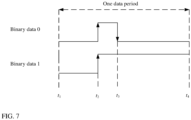
- Binary data 0 and binary data 1 have different signal waveforms in one data period, therefore, the first device may pack one bit of data in one data period, so that different data can have different signal waveforms after being packed.
- FIG. 7 shows a waveform corresponding to binary data 0 and a waveform corresponding to binary data 1 in one data period. It can be learned from FIG. 7 that binary data 0 and binary data 1 present different waveforms in one data period. Specifically, FIG. 7 is used as an example.
- One data period is a duration from a moment t1 to a moment t4.
- a low-level signal is at the moment t1 to the moment t2, at the moment t2 the low level jumps to a high level (that is, a signal rising edge), the high-level signal is at the moment t2 to the moment t3 are, at the moment t3 the high level jumps to the low level (that is, a signal falling edge), and the low-level signal is at the moment t3 to the moment t4.
- a signal waveform corresponding to binary data 0 includes a signal rising edge and a signal falling edge.
- a low-level signal is at the moment t1 to the moment t2, at the moment t2 the low level jumps to a high level (that is, a signal rising edge), and the high-level signal is at the moment t2 to the moment t4. Therefore, in a data period, a signal waveform corresponding to binary data 0 includes a signal rising edge, but does not include a signal falling edge.
- a signal rising edge exists in signal waveforms corresponding to binary data 0 and binary data 1. This is because: before the target signal cable starts to transmit data, the target signal cable is in a power-off idle state, which is equivalent to outputting a low level in this case, that is, a low level signal is at the moment t1 to the moment t2; and when the target signal cable starts to transmit data, the target signal cable is in a power-on working state, which is equivalent to outputting a high level in this case.
- both the signal waveform corresponding to binary data 0 and the signal waveform corresponding to binary data 1 jumps from a low level to a high level, that is, a signal rising edge occurs at the moment t2.
- a signal rising edge occurs at the moment t2.
- the data period is preset by the user, and the data period may be obtained as follows: The user determines, based on internal master clocks of the first device and the second device, a working clock (referred to as a working clock) that can implement communication between the first device and the second device, and then determines that at least S working clocks are required to ensure that the signal waveform corresponding to binary data 0 is different from the signal waveform corresponding to binary data 1, that is, at least S working clocks are required to ensure that the signal waveform corresponding to binary data 0 includes a signal rising edge and a signal falling edge, and the signal waveform corresponding to binary data 1 includes a signal rising edge but does not include a signal falling edge.
- a working clock referred to as a working clock
- a value of one data period is equal to duration corresponding to the S working clocks, where S > 0 and S is a positive integer.
- the signal waveform corresponding to binary data 0 should further include a waveform corresponding to a segment of low-level signals before the signal rising edge and a waveform corresponding to a segment of low-level signals after the signal falling edge.
- the waveform corresponding to binary data 1 should further include a waveform corresponding to a segment of low-level signals before the signal rising edge and a waveform corresponding to a segment of high-level signals after the signal rising edge.
- a waveform corresponding to a segment of low-level signals before the signal rising edge and a waveform corresponding to a segment of high-level signals after the signal rising edge.
- the first device and the second device are CPLD chips, and an internal master clock of the CPLD chip is 25 mega Hertz (mega Hertz, MHz). Therefore, the first device and the second device may use a 25 MHz internal master clock as a working clock for communication. It is found through testing that, as shown in FIG. 8 , binary data 0 is at a low level in a first to third master clock period (that is, 25 MHz), is at a high level in a fourth master clock period, and is at a low level in a fifth to sixteenth master clock period; and binary data 1 is at a low level in a first to third master clock period, and is at a high level in a fourth to sixteenth master clock period.
- binary data 0 is at a low level in a first to third master clock period (that is, 25 MHz)
- binary data 1 is at a low level in a first to third master clock period, and is at a high level in a fourth to sixteenth master clock period.
- the internal master clocks of the first device and the second device may be selected as the working clocks.
- the working clock of the first device may be approximately equal to the working clock of the second device in a frequency multiplication manner, and the approximately equal working clocks are used as the working clocks for communication between the first device and the second device.
- an objective of approximately equal or totally equal working clocks of the first device and the second device is: Because the first device packs one bit of data in one data period, the second device needs to collect one bit of data in one data period, so that the second device can accurately receive the data sent by the first device.
- S103 The first device sequentially sends each bit of packed data to the second device through the target signal cable.
- packed binary data 0 is a signal segment including a signal rising edge and a signal falling edge.
- packed binary data 1 is a signal that includes a signal rising edge but does not include a signal falling edge.
- the second device receives, through the target signal cable, each bit of the packed data sent by the first device, and determines each bit of the data based on a signal waveform corresponding to each bit of the packed data, to obtain the at least one target data packet.
- any bit of the packed data sent by the first device is used as an example.
- the second device detects that a signal waveform corresponding to a bit of the packed data is on a rising edge, the second device starts timing, and collects data at a preset moment.
- the second device determines that the collected data is binary data 0.
- the second device determines that the collected data is binary data 1.
- the second device may determine each bit of the data sent by the first device, to obtain the at least one target data packet.
- the preset moment is a preset working clock period.
- FIG. 8 is used as an example.
- the preset moment may be any one of the fifth master clock period to the sixteenth master clock period shown in FIG. 8 .
- the second device detects a signal rising edge through the target signal cable, the second device starts the internal master clock to start timing, and starts collecting data after X master clock periods. If the second device collects a low level, the second device determines that the collected data is binary data 0, and if the second device collects a high level, the second device determines that the collected data is binary data 1. 2 ⁇ X ⁇ 13, and X is a positive integer.
- the second device when the second device detects a signal rising edge, the second device starts timing, that is, the second device starts timing from the fourth master clock period in FIG. 8 .
- 2 ⁇ X ⁇ 13 is equivalent to any master clock period from the fifth master clock period to the sixteenth master clock period in FIG. 8 .
- the second device parses the at least one target data packet based on a preset format, to obtain the multi-bit target data in the at least one target data packet.
- the second device after the first device sends all the at least one target data packet to the second device through the target signal cable, the second device obtains multi-bit data. Then, the second device determines, based on the preset format, which data in the multi-bit data forms a data packet header, to determine which data in the multi-bit data is target data.
- the second device after obtaining the multi-bit data, determines locations of a plurality of data packet headers in the multi-bit data based on consecutive multi-bit first identification data included in the data packet header in the preset format, and then determines each data segment in a corresponding target data packet and target data in each data segment based on a location of each data packet header, to obtain target data in each target data packet, and further obtain the multi-bit target data.
- the second device After receiving the multi-bit data, the second device first determines locations of five bits of consecutive binary data 1 in the multi-bit data, to determine a location of the data packet header and determine that the data packet header is "111110". Then, four bits of data after the data packet header are extracted, that is, target data "0101" in a first data segment, and it is determined that the first data segment is "01010".
- the communication method shown in FIG. 4 may be applied to data communication between chips.
- the first device includes a first chip
- the second device includes a second chip.
- a type of the first chip may be the same as that of the second chip.
- both the first chip and the second chip are CPLD chips.
- a type of the first chip may be different from that of the second chip.
- the first chip is a CPLD chip
- the second chip is a digital signal processing (digital signal processing, DSP) chip.
- DSP digital signal processing
- the communication method shown in FIG. 4 may be further applied to a cable anti-misinsertion scenario, that is, whether a target signal cable between the first device and the second device is correctly connected is determined.
- the first device and the second device may be chips, boards, and the like. This is not specifically limited herein. For a specific process, refer to detailed description in step 21 to step 23 below.
- step 11 to step 13 and step 21 to step 23 two application scenarios of the communication method shown in FIG. 4 .
- Step 11 Design a board schematic diagram.
- one or two signal cables are designed between the first chip and the second chip based on a requirement for communication between the first chip and the second chip.
- one signal cable may be designed between a chip A and a chip B.
- two signal cables may be designed between the first chip and the second chip.
- the first chip and the second chip may be disposed on a same board, or may be disposed on different boards, which is not specifically limited herein.
- Step 12 Write logic code of the board.
- related code for data receiving and sending between the first chip and the second chip is written according to a communication protocol (including data packing, a data packet structure, data receiving, and the like) involved in the foregoing content.
- a communication protocol including data packing, a data packet structure, data receiving, and the like
- Step 13 Prepare the board.
- the written logic code is burnt into the first chip and the second chip based on a requirement.
- Step 14 Test the board.
- a program is run to test and improve a signal waveform on a signal cable between the first chip and the second chip, to ensure that a hardware link between the first chip and the second chip is stable. Then, whether data communication between the first chip and the second chip is normal is verified by sending and receiving data (for example, determining whether sent data is consistent with received data). When data communication between the first chip and the second chip is normal, it indicates that data communication can be implemented between the first chip and the second chip.
- Step 21 The first device sends the at least one target data packet to the second device.
- the at least one target data packet includes the multi-bit target data, the multi-bit target data includes identification information of the target signal cable, and the identification information of the target signal cable is used to indicate the target signal cable.
- the identification information of the target signal cable includes a cable number of the target signal cable.
- Step 22 The second device receives the at least one target data packet sent by the first device, and parses the at least one target data packet to obtain the multi-bit target data included in the at least one target data packet.
- Step 23 The second device determines whether the identification information of the target signal cable included in the multi-bit target data matches preset information. If the identification information of the target signal cable matches the preset information, the second device determines that the target signal cable is correctly connected; and if the identification information of the target signal cable does not match the preset information, the second device determines that the target signal cable is incorrectly connected.
- the second device stores the preset information
- the preset information includes identification information of at least one signal cable and connection information of the at least one signal cable
- the identification information of the at least one signal cable is in a one-to-one correspondence with the connection information of the at least one signal cable.
- Both identification information of a signal cable and connection information of a signal cable are used to indicate the signal cable.
- the identification information of the signal cable may be a cable number of the signal cable
- the connection information of the signal cable may include information about two ports connected to the signal cable, or may be information about one of the two ports connected to the signal cable (the port is not a port that stores the preset information on the second device). This is not specifically limited herein.
- the identification information of the at least one signal cable includes the identification information of the target signal cable
- the connection information of the at least one signal cable includes connection information of the target signal cable
- the connection information of the target signal cable includes information about a port 1 of the first device and information about a port 2 of the second device, or the connection information of the target signal cable is information about a port 1 of the first device. That the identification information of the target signal cable matches the preset information indicates that the identification information of the target signal cable is consistent with identification information of any signal cable in the preset information, and a port indicated by connection information of a corresponding signal cable includes the port 1 of the first device (a port that sends the identification information of the target signal cable).
- the second device may send alarm information, to notify the user that the target signal cable is incorrectly connected, so that the user can find that the target signal cable is incorrectly connected in a timely manner, and reconnect the target signal cable, and data communication between the first device and the second device is more accurate and secure.
- a number of a target cable is 0001.
- the second device matches the target data with the preset information, and determines that the target data is consistent with the number of the target signal cable in the preset information, and that the target data is sent through the port 1 of the first device, which meets the connection information of the target signal cable in the preset information. In this case, the second device determines that the target signal cable is correctly connected.
- step 21 to step 23 merely describe a method for determining whether a cable (that is, the target signal cable) between the first device and the second device is correctly connected.
- whether the cable is correctly connected may also be determined by using the method described in step 21 to step 23.
- whether all cables are correctly connected can be effectively and accurately determined by using the method described in step 21 to step 23, thereby implementing a function of cable anti-misinsertion.
- FIG. 9 shows a schematic diagram of a structure of a first device according to an embodiment of this application.
- the first device includes a data packet construction unit 110, a data packing unit 120, and a data transceiver unit 130.
- the data packet construction unit 110 is configured to construct to-be-sent multi-bit target data into at least one target data packet based on a preset format, where each target data packet includes at least one bit of the target data and multi-bit identification data, and the multi-bit identification data in each target data packet is used to indicate a quantity and locations of target data in a corresponding target data packet.
- the data packing unit 120 is configured to pack each bit of data in the at least one target data packet, so that different data has different signal waveforms after being packed.
- the data transceiver unit 130 is configured to sequentially send each bit of packed data to the second device through the target signal cable.
- a signal waveform corresponding to the one bit of data includes a signal rising edge and a signal falling edge; and when one bit of data in the at least one target data packet is binary data 1, in one data period, a signal waveform corresponding to the one bit of data includes a signal rising edge and does not include a signal falling edge.
- the multi-bit identification data includes multi-bit first identification data multi-bit and second identification data, and the first identification data is different from the second identification data.
- the preset format includes: the target data packet includes a data packet header and at least one data segment, the data packet header includes consecutive same bits of multi-bit first identification data and at least one bit of the second identification data, each data segment in the at least one data segment includes at least one bit of the target data and at least one bit of the second identification data, and a quantity of the consecutive same bits of multi-bit first identification data in the data packet header is greater than a quantity of the at least one bit of the target data in each data segment.
- the first device may be a chip, or may be a board including a chip, and the like. This is not specifically limited herein.
- the second device may be a chip, or may be a board including a chip, and the like. This is not specifically limited herein.
- the first device and the second device may be a same device, or may be different devices.
- the preset format in this embodiment of this application, a signal waveform corresponding to each bit of the packed data, and the like are not described in detail.
- a signal waveform corresponding to each bit of the packed data and the like are not described in detail.
- the foregoing embodiment also does not describe in detail a process in which the data packet construction unit 110 constructs the target data packet and a process in which the data packing unit 120 packs data in the first device.
- the data packet construction unit 110 constructs the target data packet
- the data packing unit 120 packs data in the first device.
- the first device in this embodiment of this application is described merely by using division of the foregoing functional modules as an example.
- the foregoing functions may be allocated to different functional modules for implementation based on a requirement, that is, an internal structure of the first device is divided into different functional modules to implement all or some of the functions described above.
- the first device provided in the foregoing embodiment and the first device in the foregoing method embodiment belong to a same concept. For a specific implementation process, refer to the foregoing method embodiment. Details are not described herein again.
- FIG. 10 shows a schematic diagram of a structure of a second device according to an embodiment of this application.
- the second device includes a data transceiver unit 210 and a data packet parsing unit 220.
- the data transceiver unit 210 is configured to receive, through a target signal cable, each bit of packed data sent by a first device, and determine each bit of the data based on a signal waveform corresponding to each bit of the packed data, to obtain at least one target data packet.
- the data packet parsing unit 220 is configured to parse the at least one target data packet based on a preset format, to obtain multi-bit target data in the at least one target data packet.
- the data transceiver unit 210 is specifically configured to: when it is detected that a signal waveform corresponding to each bit of the packed data is on a rising edge, start timing, and collect data at a preset moment; when a low level is collected, determine that the collected data is binary data 0; and when a high level is collected, determine that the collected data is binary data 1.
- the second device further includes a determining unit 230.
- the determining unit 230 is configured to: determine whether identification information of the target signal cable included in the multi-bit target data matches preset information, where the identification information of the target signal cable is used to indicate the target signal cable; when the identification information of the target signal cable matches the preset information, determine that the target signal cable is correctly connected; and when the identification information of the target signal cable does not match the preset information, determine that the target signal cable is incorrectly connected.
- the first device may be a chip, or may be a board including a chip, and the like. This is not specifically limited herein.
- the second device may be a chip, or may be a board including a chip, and the like. This is not specifically limited herein.
- the first device and the second device may be a same device, or may be different devices.
- the second device in this embodiment of this application is described merely by using division of the foregoing functional modules as an example.
- the foregoing functions may be allocated to different functional modules for implementation based on a requirement, that is, an internal structure of the second device is divided into different functional modules to implement all or some of the functions described above.
- the second device provided in the foregoing embodiment and the second device in the foregoing method embodiment belong to a same concept. For a specific implementation process, refer to the foregoing method embodiment. Details are not described herein again.
- FIG. 11 shows a schematic diagram of a structure of another first device according to an embodiment of this application.
- the first device includes a processor 310, a communication interface 320, and a memory 330.
- the processor 310, the communication interface 320, and the memory 330 are coupled through a bus 340.
- the processor 310 may be a central processing unit (central processing unit, CPU), a general-purpose processor, a DSP, an application specific integrated circuit (application specific integrated circuit, ASIC), a field programmable gate array (field programmable gate array, FPGA) or another programmable logic device (programmable logic device, PLD), a CPLD, a transistor logic device, a hardware component, or any combination thereof.
- the processor 310 may implement or perform various example methods described with reference to the embodiments of this application. Specifically, the processor 310 reads program code stored in the memory 330, and cooperates with the communication interface 320 to perform some or all steps of S101 to S103 and step 21.
- the memory 330 may include a volatile memory, for example, a random access memory (random access memory, RAM). Alternatively, the memory 330 may include a non-volatile memory, for example, a read only memory (read only memory, ROM), a flash memory, a hard disk drive (hard disk drive, HDD), or a solid state drive (solid state drive, SSD). Alternatively, the memory 330 may include a combination of the foregoing types of memories.
- the memory 330 may store program code and program data.
- the program code includes code of some or all units in the first device shown in FIG. 9 , for example, code of the data packet construction unit 110, code of the data packing unit 120, and code of the data transceiver unit 130.
- the program data is data generated in a process of running a program by the first device shown in FIG. 9 , for example, the target data, the first identification data, and the second identification data.
- the bus 340 may be a controller area network (controller area network, CAN) or another implementation internal bus.
- the bus 340 may be classified into an address bus, a data bus, a control bus, and the like. For ease of representation, only one bold line is used to represent the bus in FIG. 11 , but this does not mean that there is only one bus or only one type of bus.
- the first device in this embodiment of this application is configured to perform the method performed by the first device in the foregoing method embodiment, and belongs to a same concept as the foregoing method embodiment.
- the foregoing method embodiment For a specific implementation process, refer to the foregoing method embodiment. Details are not described herein again.
- FIG. 12 shows a schematic diagram of a structure of another second device according to an embodiment of this application.
- the second device includes a processor 410, a communication interface 420, and a memory 430.
- the processor 410, the communication interface 420, and the memory 430 are coupled through a bus 440.
- the processor 410 may be a CPU, a general-purpose processor, a DSP, an ASIC, an FPGA, a PLD, a CPLD, a transistor logic device, a hardware component, or any combination thereof.
- the processor 410 may implement or perform various example methods that are described with reference to content disclosed in this application. Specifically, the processor 410 reads program code stored in the memory 430, and cooperates with the communication interface 420 to perform some or all of S104 and S105 and step 22 and step 23.
- the communication interface 420 may be a wired interface or a wireless interface, and is configured to communicate with another module or device.
- the wired interface may be an Ethernet interface, a controller area network interface, an LIN, or a FlexRay interface.
- the wireless interface may be a cellular network interface, a wireless local area network interface, and the like.
- the communication interface 420 may be connected to another electronic device 450 (for example, a first device), to implement data communication between the first device and the second device.
- the memory 430 may include a volatile memory, for example, a RAM.
- the memory 430 may also include a non-volatile memory, for example, a ROM, a flash memory, an HDD, or an SSD.
- the memory 430 may further include a combination of the foregoing types of memories.
- the memory 430 may store program code and program data.
- the program code includes code of some or all units in the second device shown in FIG. 10 , for example, code of the data transceiver unit 210, code of the data packet parsing unit 220, and code of the determining unit 230.
- the program data is data generated by the second device in a process of running a program shown in FIG. 10 , for example, the target data, the first identification data, the second identification data, and the preset information.
- the bus 440 may be a CAN or another implementation internal bus.
- the bus 440 may be classified into an address bus, a data bus, a control bus, and the like. For ease of representation, only one bold line is used to represent the bus in FIG. 12 , but this does not mean that there is only one bus or only one type of bus.
- the second device in this embodiment of this application is configured to perform the method performed by the second device in the foregoing method embodiment, and belongs to a same concept as the foregoing method embodiment.
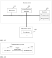
- An embodiment of this application further provides a communication system.
- the communication system shown in FIG. 13 includes a first device 510 and a second device 520.
- the first device 510 and the second device 520 are connected through a target signal cable.
- the first device 510 may be the first device shown in FIG. 9 , or may be the first device shown in FIG. 11 .
- the first device 510 is configured to perform the method performed by the first device in the foregoing method embodiments.
- the second device 520 may be the second device shown in FIG. 10 , or may be the second device shown in FIG. 12 .
- the second device 520 is configured to perform the method performed by the second device in the foregoing method embodiments.
- For a specific implementation process of the second device 520 refer to the foregoing method embodiments. Details are not described herein again.
- This application further provides a computer-readable storage medium.
- the computer-readable storage medium stores computer instructions.
- the computer instructions run on a computing device (for example, the first device shown in FIG. 9 or FIG. 11 )
- the computing device is enabled to perform the method performed by the first device in the foregoing method embodiments.
- This application further provides another computer-readable storage medium.
- the computer-readable storage medium stores computer instructions, and when the computer instructions run on a computing device (for example, the second device shown in FIG. 10 or FIG. 12 ), the computing device is enabled to perform the method performed by the second device in the foregoing method embodiments.
- All or some of the foregoing embodiments may be implemented by using software, hardware, firmware, or any combination thereof.
- software is used to implement the embodiments, all or a part of the embodiments may be implemented in a form of a computer program product.
- the computer program product includes one or more computer instructions.
- computer program instructions When computer program instructions are loaded and executed on a computer, the procedure or functions according to the embodiments of this application are all or partially generated.
- the computer may be a general-purpose computer, a dedicated computer, a computer network, or another programmable apparatus.
- the computer instructions may be stored in a computer-readable storage medium or may be transmitted from a computer-readable storage medium to another computer-readable storage medium.
- the computer instructions may be transmitted from a website, computer, server, or data center to another website, computer, server, or data center in a wired (for example, a coaxial cable, an optical fiber, or a digital subscriber line) or a wireless (for example, infrared, radio, or microwave) manner.
- the computer-readable storage medium may be any usable medium accessible by a computer, or a data storage device, for example, a server or a data center, integrating one or more usable media.
- the usable medium may be a magnetic medium (for example, a floppy disk, a storage disk, or a magnetic tape), an optical medium (for example, a DVD), a semiconductor medium (for example, an SSD), and the like.
- the description of each embodiment has respective focuses. For a part that is not described in detail in an embodiment, refer to related description in other embodiments.
- Division into the units is merely logical function division and may be other division in actual implementation. For example, a plurality of units or components may be combined or integrated into another system, or some features may be ignored or not performed.
- the displayed or discussed mutual indirect couplings or direct couplings or communication connections may be implemented by using some interfaces.
- the indirect couplings or communication connections between the apparatuses or units may be implemented in electronic or other forms.
- the foregoing units described as separate parts may or may not be physically separate, and parts displayed as units may or may not be physical units, may be located in one position, or may be distributed on a plurality of network units. Some or all of the units may be selected based on actual requirements to achieve the objectives of the solutions of the embodiments of this application.
- functional units in the embodiments of this application may be integrated into one processing unit, or each of the units may exist alone physically, or two or more units are integrated into one unit.
- the integrated unit may be implemented in a form of hardware, or may be implemented in a form of a software functional unit.
- the integrated unit When the foregoing integrated unit is implemented in the form of a software functional unit and sold or used as an independent product, the integrated unit may be stored in a computer-readable storage medium.
- the computer software product is stored in a storage medium and includes several instructions for instructing a computer device (which may be a personal computer, a server, a network device, and the like) to perform all or a part of the steps of the methods described in embodiments of this application.
- the foregoing storage medium may include: any medium that can store program code, such as a USB flash disk, a removable hard disk, a read-only memory, a random access memory, a magnetic disk, or an optical disc.
Landscapes
- Engineering & Computer Science (AREA)
- Computer Networks & Wireless Communication (AREA)
- Signal Processing (AREA)
- Computer Security & Cryptography (AREA)
- Theoretical Computer Science (AREA)
- General Engineering & Computer Science (AREA)
- Physics & Mathematics (AREA)
- General Physics & Mathematics (AREA)
- General Health & Medical Sciences (AREA)
- Medical Informatics (AREA)
- Computing Systems (AREA)
- Health & Medical Sciences (AREA)
- Dc Digital Transmission (AREA)
- Communication Control (AREA)
Claims (11)
- Procédé de communication, appliqué à un premier dispositif (510) et à un second dispositif (520), dans lequel le premier dispositif (510) et le second dispositif (520) mettent en œuvre une communication de données selon un protocole de communication série asynchrone à ligne unique par le biais d'un câble de signal cible, et le procédé comprend :la construction (S101), par le premier dispositif (510), de données cibles multibits à envoyer dans au moins un paquet de données cibles sur la base d'un format prédéfini, dans lequel chaque paquet de données cibles comprend au moins un bit des données cibles et des données d'identification multibits, et les données d'identification multibits dans chaque paquet de données cibles sont utilisées pour indiquer une quantité et des emplacements de données cibles dans un paquet de données cibles correspondant ;la mise en paquet (S102), par le premier dispositif (510), de chaque bit de données dans l'au moins un paquet de données cibles, de sorte que des données différentes ont des formes d'onde de signal différentes après avoir été mises en paquet ; et l'envoi séquentiel (S103), par le premier dispositif (510), de chaque bit de données mises en paquet au second dispositif (520) par le biais du câble de signal cible ;dans lequel, lorsqu'un bit de données dans l'au moins un paquet de données cibles représente des données binaires 0, dans une période de données, une forme d'onde de signal correspondant au bit de données comprend un front ascendant de signal et un front descendant de signal ; et lorsqu'un bit de données dans l'au moins un paquet de données cibles représente des données binaires 1, dans une période de données, une forme d'onde de signal correspondant à un bit de données comprend un front ascendant de signal et ne comprend pas de front descendant de signal ;dans lequel les données d'identification multibits comprennent des premières données d'identification multibits et des secondes données d'identification, et les premières données d'identification multibits sont différentes des secondes données d'identification ;le format prédéfini comprend : le paquet de données cibles comprend un en-tête de paquet de données et au moins un segment de données, l'en-tête de paquet de données comprend des bits consécutifs identiques de premières données d'identification multibits et au moins un bit des secondes données d'identification, chaque segment de données dans l'au moins un segment de données comprend au moins un bit des données cibles et au moins un bit des secondes données d'identification, et une quantité des bits consécutifs identiques de premières données d'identification multibits dans l'en-tête de paquet de données est supérieure à une quantité de l'au moins un bit des données cibles dans chaque segment de données ;la quantité des bits identiques dans les premières données d'identification multibits dans l'en-tête de paquet de données indique la quantité de bits des données cibles dans chaque segment de données ; etl'emplacement des données cibles dans chaque segment de données par rapport aux secondes données d'identification multibits dans chaque segment de données est indiqué par l'emplacement des secondes données d'identification multibits par rapport aux premières données d'identification multibits dans l'en-tête de paquet de données ; dans lequellorsque, dans l'en-tête de paquet de données, les secondes données d'identification multibits suivent les premières données d'identification multibits, cela indique l'emplacement des données cibles à ajouter aux secondes données d'identification multibits dans chaque segment de données ; oulorsque, dans l'en-tête de paquet de données, les secondes données d'identification multibits sont ajoutées aux premières données d'identification multibits, cela indique l'emplacement des données cibles qui doivent suivre les secondes données d'identification multibits dans chaque segment de données.
- Procédé selon la revendication 1, dans lequel le procédé comprend en outre :la réception (S104), par le second dispositif (520) par le biais du câble de signal cible, de chaque bit des données mises en paquet envoyées par le premier dispositif (510), et la détermination de chaque bit des données sur la base d'une forme d'onde de signal correspondant à chaque bit des données mises en paquet, afin d'obtenir l'au moins un paquet de données cibles ; etl'analyse (S105), par le second dispositif (520), de l'au moins un paquet de données cibles, sur la base du format prédéfini, afin d'obtenir les données cibles multibits.
- Procédé selon la revendication 2, dans lequel la détermination, par le second dispositif (520), de chaque bit des données sur la base d'une forme d'onde de signal correspondant à chaque bit des données mises en paquet comprend :lorsque le second dispositif (520) détecte que la forme d'onde de signal correspondant à chaque bit des données mises en paquet est sur un front ascendant, le début, par le second dispositif (520), de la temporisation, et la collecte de données à un moment prédéfini ;lorsque le second dispositif (520) collecte un niveau bas, le fait de déterminer, par le second dispositif (520), que les données collectées sont des données binaires 0 ; et lorsque le second dispositif (520) collecte un niveau élevé, le fait de déterminer, par le second dispositif (520), que les données collectées sont des données binaires 1.
- Procédé selon l'une quelconque des revendications 1 à 3, dans lequel le procédé est appliqué à une communication de données entre puces, le premier dispositif (510) comprend une première puce, et le second dispositif (520) comprend une seconde puce.
- Procédé selon quelconque l'une des revendications 1 à 4, dans lequel le procédé est appliqué pour déterminer si le câble de signal cible est correctement connecté, les données cibles multibits comprennent des informations d'identification du câble de signal cible, les informations d'identification du câble de signal cible sont utilisées pour indiquer le câble de signal cible, et après que le second dispositif (520) obtient les données cibles multibits dans le paquet de données cibles, le procédé comprend en outre :le fait de déterminer, par le second dispositif (520), si les informations d'identification du câble de signal cible comprises dans les données cibles multibits correspondent à des informations prédéfinies ;lorsque les informations d'identification du câble de signal cible correspondent aux informations prédéfinies, le fait de déterminer, par le second dispositif (520), que le câble de signal cible est correctement connecté ; etlorsque les informations d'identification du câble de signal cible ne correspondent pas aux informations prédéfinies, le fait de déterminer, par le second dispositif (520), que le câble de signal cible n'est pas connecté correctement.
- Premier dispositif (510), dans lequel le premier dispositif (510) et un second dispositif (520) sont configurés pour mettre en œuvre une communication de données selon un protocole de communication série asynchrone à ligne unique par le biais d'un câble de signal cible, et le premier dispositif (510) comprend une unité de construction de paquets de données (110), une unité de mise en paquet de données (120), et une unité d'émission-réception de données (130, 210), dans lequel l'unité de construction de paquet de données (110) est configurée pour construire des données cibles multibits à envoyer dans au moins un paquet de données cibles sur la base d'un format prédéfini, dans lequel chaque paquet de données cibles comprend au moins un bit des données cibles et des données d'identification multibits, et les données d'identification multibits dans chaque paquet de données cibles sont utilisées pour indiquer une quantité et des emplacements de données cibles dans un paquet de données cibles correspondant ;l'unité de mise en paquet de données (120) est configurée pour mettre en paquet chaque bit de données dans l'au moins un paquet de données cible, de sorte que des données différentes ont des formes d'onde de signal différentes après avoir été mises en paquet ; etl'unité d'émission-réception de données (130, 210) est configurée pour envoyer de manière séquentielle chaque bit de données mises en paquet au second dispositif (520) par le biais du câble de signal cible ;dans lequel, lorsqu'un bit de données dans l'au moins un paquet de données cibles représente des données binaires 0, dans une période de données, une forme d'onde de signal correspondant à un bit de données comprend un front ascendant de signal et un front descendant de signal ; et lorsqu'un bit de données dans l'au moins un paquet de données cibles représente des données binaires 1, dans une période de données, une forme d'onde de signal correspondant à un bit de données comprend un front ascendant de signal et ne comprend pas de front descendant de signal ; dans lequel les données d'identification multibits comprennent des premières données d'identification multibits et des secondes données d'identification, et les premières données d'identification multibits sont différentes des secondes données d'identification ; etle format prédéfini comprend : le paquet de données cibles comprend un en-tête de paquet de données et au moins un segment de données, l'en-tête de paquet de données comprend des bits consécutifs identiques de premières données d'identification multibits et au moins un bit des secondes données d'identification, chaque segment de données dans l'au moins un segment de données comprend au moins un bit des données cibles et au moins un bit des secondes données d'identification, et une quantité de bits consécutifs identiques de premières données d'identification multibits dans l'en-tête de paquet de données est supérieure à une quantité de l'au moins un bit des données cibles dans chaque segment de données ; etla quantité de bits identiques dans les premières données d'identification multibits dans l'en-tête de paquet de données indique la quantité de bits des données cibles dans chaque segment de données ; et l'emplacement des données cibles dans chaque segment de données par rapport aux secondes données d'identification multibits dans chaque segment de données est indiqué par l'emplacement des secondes données d'identification multibits par rapport aux premières données d'identification multibits dans l'en-tête de paquet de données ; dans lequel lorsque, dans l'en-tête de paquet de données, les secondes données d'identification multibits suivent les premières données d'identification multibits, cela indique l'emplacement des données cibles à ajouter aux secondes données d'identification multibits dans chaque segment de données ; oulorsque, dans l'en-tête de paquet de données, les secondes données d'identification multibits sont ajoutées aux premières données d'identification multibits, cela indique l'emplacement des données cibles qui doivent suivre les secondes données d'identification multibits dans chaque segment de données.
- Dispositif (350, 450) selon la revendication 6, dans lequel le premier dispositif (510) comprend en outre une unité d'analyse de paquet de données (220), dans lequell'unité d'émission-réception de paquets de données est en outre configurée pour recevoir, par le biais du câble de signal cible, des données multibits mises en paquet envoyées par le second dispositif (520), et pour déterminer chaque bit de données dans les données multibits mise en paquet sur la base d'une forme d'onde de signal correspondant à chaque bit de données dans les données multibits mises en paquet, afin d'obtenir au moins un paquet de données ; etl'unité d'analyse de paquet de données (220) est configurée pour analyser l'au moins un paquet de données sur la base du format prédéfini, afin d'obtenir des données cibles dans l'au moins un paquet de données.
- Dispositif (350, 450) selon la revendication 7, dans lequel l'unité d'émission-réception de données (130, 210) est spécifiquement configuré pour :lorsqu'il est détecté que la forme d'onde de signal correspondant à chaque bit des données mises en paquet est sur un front ascendant, débuter la temporisation et collecter des données à un moment prédéfini ;lorsqu'un niveau bas est collecté, déterminer que les données collectées sont des données binaires 0 ; etlorsqu'un niveau élevé est collecté, déterminer que les données collectées sont des données binaires 1.
- Premier dispositif (510), dans lequel le premier dispositif (510) comprend un processeur (310, 410) et une mémoire (330, 430), et le processeur exécute le code dans la mémoire (330, 430) pour mettre en œuvre toutes les étapes de procédé réalisées par le premier dispositif (510) selon les revendications 1 à 5.
- Support de stockage lisible par ordinateur, stockant des instructions informatiques, dans lequel les instructions informatiques sont utilisées pour mettre en œuvre toutes les étapes de procédé réalisées par le premier dispositif (510) selon les revendications 1 à 5.
- Système de communication, dans lequel le système de communication comprend un premier dispositif (510) et un second dispositif (520), le premier dispositif (510) est configuré pour mettre en œuvre toutes les étapes de procédé réalisées par le premier dispositif (510) selon les revendications 1 à 5, et le second dispositif (520) est configuré pour réaliser toutes les étapes de procédé réalisées par le second dispositif (520) selon les revendications 1 à 5.
Applications Claiming Priority (2)
| Application Number | Priority Date | Filing Date | Title |
|---|---|---|---|
| CN202011003324.2A CN114301991B (zh) | 2020-09-22 | 2020-09-22 | 通信方法、设备、系统及计算机可读存储介质 |
| PCT/CN2021/117847 WO2022062925A1 (fr) | 2020-09-22 | 2021-09-11 | Procédé, dispositif et système de communication, et support de stockage lisible par ordinateur |
Publications (3)
| Publication Number | Publication Date |
|---|---|
| EP4207643A1 EP4207643A1 (fr) | 2023-07-05 |
| EP4207643A4 EP4207643A4 (fr) | 2023-12-06 |
| EP4207643B1 true EP4207643B1 (fr) | 2025-03-26 |
Family
ID=80845001
Family Applications (1)
| Application Number | Title | Priority Date | Filing Date |
|---|---|---|---|
| EP21871296.6A Active EP4207643B1 (fr) | 2020-09-22 | 2021-09-11 | Procédé, dispositif et système de communication, et support de stockage lisible par ordinateur |
Country Status (4)
| Country | Link |
|---|---|
| US (1) | US20230231940A1 (fr) |
| EP (1) | EP4207643B1 (fr) |
| CN (1) | CN114301991B (fr) |
| WO (1) | WO2022062925A1 (fr) |
Families Citing this family (5)
| Publication number | Priority date | Publication date | Assignee | Title |
|---|---|---|---|---|
| CN114546095B (zh) * | 2022-04-25 | 2022-07-01 | 沐曦科技(北京)有限公司 | 基于多运算设备的master选择方法 |
| CN115766892A (zh) * | 2022-10-21 | 2023-03-07 | 超聚变数字技术有限公司 | 数据发送方法及接收方法 |
| CN115902710A (zh) * | 2022-10-26 | 2023-04-04 | 超聚变数字技术有限公司 | 防呆检测方法及计算设备 |
| CN115951266A (zh) * | 2022-11-16 | 2023-04-11 | 超聚变数字技术有限公司 | 一种计算系统 |
| CN116112391A (zh) * | 2022-12-30 | 2023-05-12 | 超聚变数字技术有限公司 | 一种线缆连接检测方法、配置方法和计算设备 |
Family Cites Families (20)
| Publication number | Priority date | Publication date | Assignee | Title |
|---|---|---|---|---|
| JP3136742B2 (ja) * | 1992-02-14 | 2001-02-19 | 日産自動車株式会社 | 通信装置 |
| US6853644B1 (en) * | 1999-12-22 | 2005-02-08 | Intel Corporation | Method and apparatus for driving data packets |
| CN1706139A (zh) * | 2002-10-17 | 2005-12-07 | 高通股份有限公司 | 用于在通信系统中传送和接收数据块的方法和装置 |
| CA2731269C (fr) * | 2003-12-08 | 2013-01-08 | Qualcomm Incorporated | Interface haut debit de donnees a synchronisation de liaisons amelioree |
| EP1553738A1 (fr) * | 2004-01-12 | 2005-07-13 | Thomson Licensing S.A. | Procédé et dispositif pour générer des paquets de données |
| CN101459654A (zh) * | 2007-12-14 | 2009-06-17 | 联想移动通信科技有限公司 | 一种多协议业务数据封装解析方法、接收端和发送端 |
| US8639853B2 (en) * | 2011-07-28 | 2014-01-28 | National Intruments Corporation | Programmable waveform technology for interfacing to disparate devices |
| US9136764B2 (en) * | 2012-04-19 | 2015-09-15 | Integrated Device Technology, Inc. | Apparatuses and system and method for auto-configuration of a power control system |
| US10348833B2 (en) * | 2015-03-06 | 2019-07-09 | Fuji Corporation | Multiplex communication system and work machine |
| EP3742324B1 (fr) * | 2015-09-15 | 2024-11-27 | Gatekeeper Ltd. | Système et procédé permettant de se connecter en toute sécurité à un dispositif périphérique |
| CN105404607B (zh) * | 2015-11-20 | 2018-02-13 | 英业达科技有限公司 | 通用串行输入输出的数据传输方法 |
| US10225187B2 (en) * | 2017-03-22 | 2019-03-05 | Cisco Technology, Inc. | System and method for providing a bit indexed service chain |
| US10635630B2 (en) * | 2018-08-09 | 2020-04-28 | Qualcomm Incorporated | Flexible protocol and associated hardware for one-wire radio frequency front-end interface |
| US12464041B2 (en) * | 2019-02-13 | 2025-11-04 | Telefonaktiebolaget Lm Ericsson (Publ) | Industrial automation with 5G and beyond |
| CN110244604A (zh) * | 2019-05-29 | 2019-09-17 | 北京大豪科技股份有限公司 | 数据传输方法、装置、电子设备及存储介质 |
| CN110247734B (zh) * | 2019-06-18 | 2021-11-23 | 合肥奕斯伟集成电路有限公司 | 一种数据传输方法、装置及电子设备 |
| CN110659232B (zh) * | 2019-09-12 | 2021-06-29 | 苏州浪潮智能科技有限公司 | 一种事件信息传输方法、装置、设备及存储介质 |
| US20210286744A1 (en) * | 2020-03-16 | 2021-09-16 | Hewlett Packard Enterprise Development Lp | Programmable input/output port |
| CN111090268B (zh) * | 2020-03-24 | 2020-06-12 | 上海飞旗网络技术股份有限公司 | 基于线程划分的数据采集方法、装置及数据采集设备 |
| JP2022052901A (ja) * | 2020-09-24 | 2022-04-05 | ローランド株式会社 | 無線通信装置、電子機器および無線通信方法 |
-
2020
- 2020-09-22 CN CN202011003324.2A patent/CN114301991B/zh active Active
-
2021
- 2021-09-11 EP EP21871296.6A patent/EP4207643B1/fr active Active
- 2021-09-11 WO PCT/CN2021/117847 patent/WO2022062925A1/fr not_active Ceased
-
2023
- 2023-03-21 US US18/187,173 patent/US20230231940A1/en active Pending
Also Published As
| Publication number | Publication date |
|---|---|
| CN114301991A (zh) | 2022-04-08 |
| CN114301991B (zh) | 2023-10-20 |
| WO2022062925A1 (fr) | 2022-03-31 |
| US20230231940A1 (en) | 2023-07-20 |
| EP4207643A1 (fr) | 2023-07-05 |
| EP4207643A4 (fr) | 2023-12-06 |
Similar Documents
| Publication | Publication Date | Title |
|---|---|---|
| EP4207643B1 (fr) | Procédé, dispositif et système de communication, et support de stockage lisible par ordinateur | |
| US8099537B2 (en) | Method, device, and system for transmitting data fragments over multiple transmission lines and techniques for stopping data transmission | |
| US10241953B2 (en) | Dynamic data-link selection over common physical interface | |
| CN106464559B (zh) | 用于分布式控制系统的高速嵌入式协议 | |
| CN101770443B (zh) | 一种内部集成电路总线时序调节方法、相应装置及系统 | |
| US9258244B1 (en) | Protocol for communications in potentially noisy environments | |
| US20130235944A1 (en) | Information processing apparatus, serial communication system, method of initialization of communication therefor, and serial communication apparatus | |
| CN101937253A (zh) | 用于时钟同步的机制 | |
| JP2017525200A (ja) | リンクレイヤ/物理レイヤ(phy)シリアルインターフェース | |
| CN101834715B (zh) | 一种数据处理方法及数据处理系统以及数据处理装置 | |
| CN113852533A (zh) | 一种多通道数据通信系统、方法及电子设备 | |
| CN117687949A (zh) | 数据通信方法、装置、电子设备及非易失性存储介质 | |
| US20180083800A1 (en) | Aggregation Device, System, And Method Thereof | |
| US11169947B2 (en) | Data transmission system capable of transmitting a great amount of data | |
| WO2026016562A1 (fr) | Procédé de transmission de données et dispositif informatique | |
| CN113890783A (zh) | 一种数据收发系统、方法、电子设备及存储介质 | |
| US12436911B2 (en) | Interface device and computing system including the same | |
| CN117193473A (zh) | 忽略时钟误差的数据交互方法、系统、终端及存储介质 | |
| CN117112480B (zh) | 一种两线通信方法、装置及芯片 | |
| CN103106162B (zh) | 逻辑器件及其mdio接口通信方法 | |
| CN217428141U (zh) | 网卡、通信设备及网络安全系统 | |
| US8914554B2 (en) | Communication network device that compares first and second identification number of packet to determine if they are in conformance or non-conformance with self-ID packet | |
| JP6596901B2 (ja) | データ転送制御装置及びそれを用いた電子機器 | |
| CN116361095B (zh) | 功耗验证方法、系统、设备及存储介质 | |
| CN113220609B (zh) | 信号收发系统与方法 |
Legal Events
| Date | Code | Title | Description |
|---|---|---|---|
| STAA | Information on the status of an ep patent application or granted ep patent |
Free format text: STATUS: THE INTERNATIONAL PUBLICATION HAS BEEN MADE |
|
| PUAI | Public reference made under article 153(3) epc to a published international application that has entered the european phase |
Free format text: ORIGINAL CODE: 0009012 |
|
| STAA | Information on the status of an ep patent application or granted ep patent |
Free format text: STATUS: REQUEST FOR EXAMINATION WAS MADE |
|
| 17P | Request for examination filed |
Effective date: 20230330 |
|
| AK | Designated contracting states |
Kind code of ref document: A1 Designated state(s): AL AT BE BG CH CY CZ DE DK EE ES FI FR GB GR HR HU IE IS IT LI LT LU LV MC MK MT NL NO PL PT RO RS SE SI SK SM TR |
|
| REG | Reference to a national code |
Ref country code: DE Free format text: PREVIOUS MAIN CLASS: H99Z9999999999 Ipc: G06F0013420000 Ref country code: DE Ref legal event code: R079 Ref document number: 602021028297 Country of ref document: DE Free format text: PREVIOUS MAIN CLASS: H99Z9999999999 Ipc: G06F0013420000 |
|
| A4 | Supplementary search report drawn up and despatched |
Effective date: 20231108 |
|
| RIC1 | Information provided on ipc code assigned before grant |
Ipc: H04L 67/12 20220101ALI20231102BHEP Ipc: H04L 69/22 20220101ALI20231102BHEP Ipc: H04L 69/10 20220101ALI20231102BHEP Ipc: H04L 12/40 20060101ALI20231102BHEP Ipc: G06F 13/42 20060101AFI20231102BHEP |
|
| DAV | Request for validation of the european patent (deleted) | ||
| DAX | Request for extension of the european patent (deleted) | ||
| GRAP | Despatch of communication of intention to grant a patent |
Free format text: ORIGINAL CODE: EPIDOSNIGR1 |
|
| STAA | Information on the status of an ep patent application or granted ep patent |
Free format text: STATUS: GRANT OF PATENT IS INTENDED |
|
| RIC1 | Information provided on ipc code assigned before grant |
Ipc: H04L 67/12 20220101ALI20241120BHEP Ipc: H04L 69/22 20220101ALI20241120BHEP Ipc: G06F 13/42 20060101AFI20241120BHEP |
|
| INTG | Intention to grant announced |
Effective date: 20241129 |
|
| GRAS | Grant fee paid |
Free format text: ORIGINAL CODE: EPIDOSNIGR3 |
|
| GRAA | (expected) grant |
Free format text: ORIGINAL CODE: 0009210 |
|
| STAA | Information on the status of an ep patent application or granted ep patent |
Free format text: STATUS: THE PATENT HAS BEEN GRANTED |
|
| AK | Designated contracting states |
Kind code of ref document: B1 Designated state(s): AL AT BE BG CH CY CZ DE DK EE ES FI FR GB GR HR HU IE IS IT LI LT LU LV MC MK MT NL NO PL PT RO RS SE SI SK SM TR |
|
| REG | Reference to a national code |
Ref country code: GB Ref legal event code: FG4D |
|
| REG | Reference to a national code |
Ref country code: CH Ref legal event code: EP |
|
| REG | Reference to a national code |
Ref country code: DE Ref legal event code: R096 Ref document number: 602021028297 Country of ref document: DE |
|
| REG | Reference to a national code |
Ref country code: IE Ref legal event code: FG4D |
|
| PG25 | Lapsed in a contracting state [announced via postgrant information from national office to epo] |
Ref country code: RS Free format text: LAPSE BECAUSE OF FAILURE TO SUBMIT A TRANSLATION OF THE DESCRIPTION OR TO PAY THE FEE WITHIN THE PRESCRIBED TIME-LIMIT Effective date: 20250626 |
|
| PG25 | Lapsed in a contracting state [announced via postgrant information from national office to epo] |
Ref country code: FI Free format text: LAPSE BECAUSE OF FAILURE TO SUBMIT A TRANSLATION OF THE DESCRIPTION OR TO PAY THE FEE WITHIN THE PRESCRIBED TIME-LIMIT Effective date: 20250326 |
|
| REG | Reference to a national code |
Ref country code: LT Ref legal event code: MG9D |
|
| PG25 | Lapsed in a contracting state [announced via postgrant information from national office to epo] |
Ref country code: NO Free format text: LAPSE BECAUSE OF FAILURE TO SUBMIT A TRANSLATION OF THE DESCRIPTION OR TO PAY THE FEE WITHIN THE PRESCRIBED TIME-LIMIT Effective date: 20250626 |
|
| PG25 | Lapsed in a contracting state [announced via postgrant information from national office to epo] |
Ref country code: HR Free format text: LAPSE BECAUSE OF FAILURE TO SUBMIT A TRANSLATION OF THE DESCRIPTION OR TO PAY THE FEE WITHIN THE PRESCRIBED TIME-LIMIT Effective date: 20250326 |
|
| PG25 | Lapsed in a contracting state [announced via postgrant information from national office to epo] |
Ref country code: LV Free format text: LAPSE BECAUSE OF FAILURE TO SUBMIT A TRANSLATION OF THE DESCRIPTION OR TO PAY THE FEE WITHIN THE PRESCRIBED TIME-LIMIT Effective date: 20250326 |
|
| PG25 | Lapsed in a contracting state [announced via postgrant information from national office to epo] |
Ref country code: BG Free format text: LAPSE BECAUSE OF FAILURE TO SUBMIT A TRANSLATION OF THE DESCRIPTION OR TO PAY THE FEE WITHIN THE PRESCRIBED TIME-LIMIT Effective date: 20250326 Ref country code: GR Free format text: LAPSE BECAUSE OF FAILURE TO SUBMIT A TRANSLATION OF THE DESCRIPTION OR TO PAY THE FEE WITHIN THE PRESCRIBED TIME-LIMIT Effective date: 20250627 |
|
| REG | Reference to a national code |
Ref country code: NL Ref legal event code: MP Effective date: 20250326 |
|
| PG25 | Lapsed in a contracting state [announced via postgrant information from national office to epo] |
Ref country code: NL Free format text: LAPSE BECAUSE OF FAILURE TO SUBMIT A TRANSLATION OF THE DESCRIPTION OR TO PAY THE FEE WITHIN THE PRESCRIBED TIME-LIMIT Effective date: 20250326 |
|
| PG25 | Lapsed in a contracting state [announced via postgrant information from national office to epo] |
Ref country code: SE Free format text: LAPSE BECAUSE OF FAILURE TO SUBMIT A TRANSLATION OF THE DESCRIPTION OR TO PAY THE FEE WITHIN THE PRESCRIBED TIME-LIMIT Effective date: 20250326 |
|
| REG | Reference to a national code |
Ref country code: AT Ref legal event code: MK05 Ref document number: 1779625 Country of ref document: AT Kind code of ref document: T Effective date: 20250326 |
|
| PG25 | Lapsed in a contracting state [announced via postgrant information from national office to epo] |
Ref country code: SM Free format text: LAPSE BECAUSE OF FAILURE TO SUBMIT A TRANSLATION OF THE DESCRIPTION OR TO PAY THE FEE WITHIN THE PRESCRIBED TIME-LIMIT Effective date: 20250326 |
|
| PG25 | Lapsed in a contracting state [announced via postgrant information from national office to epo] |
Ref country code: ES Free format text: LAPSE BECAUSE OF FAILURE TO SUBMIT A TRANSLATION OF THE DESCRIPTION OR TO PAY THE FEE WITHIN THE PRESCRIBED TIME-LIMIT Effective date: 20250326 Ref country code: PT Free format text: LAPSE BECAUSE OF FAILURE TO SUBMIT A TRANSLATION OF THE DESCRIPTION OR TO PAY THE FEE WITHIN THE PRESCRIBED TIME-LIMIT Effective date: 20250728 |
|
| PGFP | Annual fee paid to national office [announced via postgrant information from national office to epo] |
Ref country code: DE Payment date: 20250730 Year of fee payment: 5 |
|
| PG25 | Lapsed in a contracting state [announced via postgrant information from national office to epo] |
Ref country code: IT Free format text: LAPSE BECAUSE OF FAILURE TO SUBMIT A TRANSLATION OF THE DESCRIPTION OR TO PAY THE FEE WITHIN THE PRESCRIBED TIME-LIMIT Effective date: 20250326 Ref country code: PL Free format text: LAPSE BECAUSE OF FAILURE TO SUBMIT A TRANSLATION OF THE DESCRIPTION OR TO PAY THE FEE WITHIN THE PRESCRIBED TIME-LIMIT Effective date: 20250326 |
|
| PG25 | Lapsed in a contracting state [announced via postgrant information from national office to epo] |
Ref country code: AT Free format text: LAPSE BECAUSE OF FAILURE TO SUBMIT A TRANSLATION OF THE DESCRIPTION OR TO PAY THE FEE WITHIN THE PRESCRIBED TIME-LIMIT Effective date: 20250326 |
|
| PG25 | Lapsed in a contracting state [announced via postgrant information from national office to epo] |
Ref country code: EE Free format text: LAPSE BECAUSE OF FAILURE TO SUBMIT A TRANSLATION OF THE DESCRIPTION OR TO PAY THE FEE WITHIN THE PRESCRIBED TIME-LIMIT Effective date: 20250326 |
|
| PG25 | Lapsed in a contracting state [announced via postgrant information from national office to epo] |
Ref country code: RO Free format text: LAPSE BECAUSE OF FAILURE TO SUBMIT A TRANSLATION OF THE DESCRIPTION OR TO PAY THE FEE WITHIN THE PRESCRIBED TIME-LIMIT Effective date: 20250326 |
|
| PG25 | Lapsed in a contracting state [announced via postgrant information from national office to epo] |
Ref country code: SK Free format text: LAPSE BECAUSE OF FAILURE TO SUBMIT A TRANSLATION OF THE DESCRIPTION OR TO PAY THE FEE WITHIN THE PRESCRIBED TIME-LIMIT Effective date: 20250326 |
|
| PG25 | Lapsed in a contracting state [announced via postgrant information from national office to epo] |
Ref country code: IS Free format text: LAPSE BECAUSE OF FAILURE TO SUBMIT A TRANSLATION OF THE DESCRIPTION OR TO PAY THE FEE WITHIN THE PRESCRIBED TIME-LIMIT Effective date: 20250726 |
|
| REG | Reference to a national code |
Ref country code: DE Ref legal event code: R097 Ref document number: 602021028297 Country of ref document: DE |
|
| PG25 | Lapsed in a contracting state [announced via postgrant information from national office to epo] |
Ref country code: DK Free format text: LAPSE BECAUSE OF FAILURE TO SUBMIT A TRANSLATION OF THE DESCRIPTION OR TO PAY THE FEE WITHIN THE PRESCRIBED TIME-LIMIT Effective date: 20250326 |
|
| PG25 | Lapsed in a contracting state [announced via postgrant information from national office to epo] |
Ref country code: CZ Free format text: LAPSE BECAUSE OF FAILURE TO SUBMIT A TRANSLATION OF THE DESCRIPTION OR TO PAY THE FEE WITHIN THE PRESCRIBED TIME-LIMIT Effective date: 20250326 |
|
| PLBE | No opposition filed within time limit |
Free format text: ORIGINAL CODE: 0009261 |
|
| STAA | Information on the status of an ep patent application or granted ep patent |
Free format text: STATUS: NO OPPOSITION FILED WITHIN TIME LIMIT |
|
| REG | Reference to a national code |
Ref country code: CH Ref legal event code: L10 Free format text: ST27 STATUS EVENT CODE: U-0-0-L10-L00 (AS PROVIDED BY THE NATIONAL OFFICE) Effective date: 20260211 |
|
| 26N | No opposition filed |
Effective date: 20260105 |