EP4209791A1 - In-situ-schwellenspannungsbestimmung einer halbleitervorrichtung - Google Patents
In-situ-schwellenspannungsbestimmung einer halbleitervorrichtung Download PDFInfo
- Publication number
- EP4209791A1 EP4209791A1 EP22210616.3A EP22210616A EP4209791A1 EP 4209791 A1 EP4209791 A1 EP 4209791A1 EP 22210616 A EP22210616 A EP 22210616A EP 4209791 A1 EP4209791 A1 EP 4209791A1
- Authority
- EP
- European Patent Office
- Prior art keywords
- voltage
- gate
- transistor
- terminal
- temperature
- Prior art date
- Legal status (The legal status is an assumption and is not a legal conclusion. Google has not performed a legal analysis and makes no representation as to the accuracy of the status listed.)
- Granted
Links
Images



Classifications
-
- G—PHYSICS
- G01—MEASURING; TESTING
- G01R—MEASURING ELECTRIC VARIABLES; MEASURING MAGNETIC VARIABLES
- G01R31/00—Arrangements for testing electric properties; Arrangements for locating electric faults; Arrangements for electrical testing characterised by what is being tested not provided for elsewhere
- G01R31/26—Testing of individual semiconductor devices
- G01R31/2607—Circuits therefor
-
- G—PHYSICS
- G01—MEASURING; TESTING
- G01R—MEASURING ELECTRIC VARIABLES; MEASURING MAGNETIC VARIABLES
- G01R31/00—Arrangements for testing electric properties; Arrangements for locating electric faults; Arrangements for electrical testing characterised by what is being tested not provided for elsewhere
- G01R31/26—Testing of individual semiconductor devices
-
- G—PHYSICS
- G01—MEASURING; TESTING
- G01R—MEASURING ELECTRIC VARIABLES; MEASURING MAGNETIC VARIABLES
- G01R31/00—Arrangements for testing electric properties; Arrangements for locating electric faults; Arrangements for electrical testing characterised by what is being tested not provided for elsewhere
- G01R31/26—Testing of individual semiconductor devices
- G01R31/2642—Testing semiconductor operation lifetime or reliability, e.g. by accelerated life tests
-
- G—PHYSICS
- G01—MEASURING; TESTING
- G01K—MEASURING TEMPERATURE; MEASURING QUANTITY OF HEAT; THERMALLY-SENSITIVE ELEMENTS NOT OTHERWISE PROVIDED FOR
- G01K13/00—Thermometers specially adapted for specific purposes
-
- G—PHYSICS
- G01—MEASURING; TESTING
- G01R—MEASURING ELECTRIC VARIABLES; MEASURING MAGNETIC VARIABLES
- G01R19/00—Arrangements for measuring currents or voltages or for indicating presence or sign thereof
- G01R19/165—Indicating that current or voltage is either above or below a predetermined value or within or outside a predetermined range of values
- G01R19/16533—Indicating that current or voltage is either above or below a predetermined value or within or outside a predetermined range of values characterised by the application
- G01R19/16538—Indicating that current or voltage is either above or below a predetermined value or within or outside a predetermined range of values characterised by the application in AC or DC supplies
-
- G—PHYSICS
- G01—MEASURING; TESTING
- G01R—MEASURING ELECTRIC VARIABLES; MEASURING MAGNETIC VARIABLES
- G01R31/00—Arrangements for testing electric properties; Arrangements for locating electric faults; Arrangements for electrical testing characterised by what is being tested not provided for elsewhere
- G01R31/26—Testing of individual semiconductor devices
- G01R31/2607—Circuits therefor
- G01R31/2608—Circuits therefor for testing bipolar transistors
- G01R31/261—Circuits therefor for testing bipolar transistors for measuring break-down voltage or punch through voltage therefor
-
- G—PHYSICS
- G01—MEASURING; TESTING
- G01R—MEASURING ELECTRIC VARIABLES; MEASURING MAGNETIC VARIABLES
- G01R31/00—Arrangements for testing electric properties; Arrangements for locating electric faults; Arrangements for electrical testing characterised by what is being tested not provided for elsewhere
- G01R31/26—Testing of individual semiconductor devices
- G01R31/2607—Circuits therefor
- G01R31/2621—Circuits therefor for testing field effect transistors, i.e. FET's
- G01R31/2623—Circuits therefor for testing field effect transistors, i.e. FET's for measuring break-down voltage therefor
-
- H—ELECTRICITY
- H02—GENERATION; CONVERSION OR DISTRIBUTION OF ELECTRIC POWER
- H02M—APPARATUS FOR CONVERSION BETWEEN AC AND AC, BETWEEN AC AND DC, OR BETWEEN DC AND DC, AND FOR USE WITH MAINS OR SIMILAR POWER SUPPLY SYSTEMS; CONVERSION OF DC OR AC INPUT POWER INTO SURGE OUTPUT POWER; CONTROL OR REGULATION THEREOF
- H02M7/00—Conversion of AC power input into DC power output; Conversion of DC power input into AC power output
- H02M7/42—Conversion of DC power input into AC power output without possibility of reversal
- H02M7/44—Conversion of DC power input into AC power output without possibility of reversal by static converters
- H02M7/48—Conversion of DC power input into AC power output without possibility of reversal by static converters using discharge tubes with control electrode or semiconductor devices with control electrode
- H02M7/53—Conversion of DC power input into AC power output without possibility of reversal by static converters using discharge tubes with control electrode or semiconductor devices with control electrode using devices of a triode or transistor type requiring continuous application of a control signal
- H02M7/537—Conversion of DC power input into AC power output without possibility of reversal by static converters using discharge tubes with control electrode or semiconductor devices with control electrode using devices of a triode or transistor type requiring continuous application of a control signal using semiconductor devices only, e.g. single switched pulse inverters
- H02M7/5387—Conversion of DC power input into AC power output without possibility of reversal by static converters using discharge tubes with control electrode or semiconductor devices with control electrode using devices of a triode or transistor type requiring continuous application of a control signal using semiconductor devices only, e.g. single switched pulse inverters in a bridge configuration
-
- H—ELECTRICITY
- H03—ELECTRONIC CIRCUITRY
- H03K—PULSE TECHNIQUE
- H03K17/00—Electronic switching or gating, i.e. not by contact-making and –breaking
- H03K17/51—Electronic switching or gating, i.e. not by contact-making and –breaking characterised by the components used
- H03K17/56—Electronic switching or gating, i.e. not by contact-making and –breaking characterised by the components used by the use, as active elements, of semiconductor devices
- H03K17/567—Circuits characterised by the use of more than one type of semiconductor device, e.g. BIMOS, composite devices such as IGBT
-
- H—ELECTRICITY
- H03—ELECTRONIC CIRCUITRY
- H03K—PULSE TECHNIQUE
- H03K17/00—Electronic switching or gating, i.e. not by contact-making and –breaking
- H03K17/51—Electronic switching or gating, i.e. not by contact-making and –breaking characterised by the components used
- H03K17/56—Electronic switching or gating, i.e. not by contact-making and –breaking characterised by the components used by the use, as active elements, of semiconductor devices
- H03K17/687—Electronic switching or gating, i.e. not by contact-making and –breaking characterised by the components used by the use, as active elements, of semiconductor devices the devices being field-effect transistors
Definitions
- This disclosure relates generally to semiconductor devices, and more specifically to methods for in situ determination of a threshold voltage of a semiconductor device.
- Incipient Fault Detection or early warning of a power device's degradation of performance due to aging or other system stress continues to be a topic of interest in systems where reliability and safety is a concern.
- the ability to interrogate a power device and monitor its health over the lifetime of the product is a powerful feature allowing system designers to anticipate failures and alert users to the need for service, prior to a catastrophic failure event.
- One device parameter associated with an incipient fault is a threshold voltage of a transistor. As power devices age, the threshold of the device will shift. The ability to precisely measure the power device threshold voltage initially and over time can provide an early indication of a power device's end of life, or that the power device no longer meets the original design specification. Traditional methods to detect changes across terminals defining the collector and emitter, or the drain and source when the power device is in an "ON" state have been used. However, such methods may be intrusive and suffer from inaccuracies.
- Embodiments described herein provide for methods for in situ determination of a threshold voltage of a device.
- the threshold voltage is compared against previously stored threshold voltage values to determine a threshold voltage shift.
- the determination of the threshold voltage shift is further used to detect an incipient fault condition of the device and furthermore a fault condition of a system within which the device operates.
- a fault condition may be determined based on a voltage shift exceeding a predetermined value, by a trend based on more than two values and/or by a dependency of multiple stored values.
- Each method includes the sourcing of a calibrated current to a first terminal (e.g. a drain or collector), which is put in a high impedance state by deactivating other devices connected thereto.
- a first device is configured in series with a second device, connected therebetween at a terminal (e.g., a source/drain or emitter/collector).
- the terminal may be charged while the first and second devices are in an "OFF" state, thereby creating a voltage across the first device.
- the terminal is charged by a calibrated current sourced from a gate driver.
- the terminal is charged by a residual voltage remaining on a DC bus capacitor connected across the combination of the series connected first and second transistors.
- An "OFF" state is detected by measuring a voltage (e.g., an open circuit bridge voltage) across the first device.
- a voltage e.g., an open circuit bridge voltage
- a series of gate levels e.g., applied as a step function or with a series of corresponding gate pulses
- the series of gate levels sequentially decreases and the last gate level exceeding the threshold voltage is stored.
- the gate terminal is insulated, for example with an Insulated Gate Field Effect Transistor (IGFET) or an Insulated Gate Bipolar Transistor (IGBT), so that the current conducted through the device or transistor (e.g. drain to source, or collector to emitter) is primarily a function of the calibrated current applied to the first terminal.
- IGFET Insulated Gate Field Effect Transistor
- Ids drain to source
- IGFET temperature compensation for other parameters (e.g., IGFET temperature), which the threshold voltage depends upon, enables the determination of the threshold voltage based on an applied gate to source (Vgs) voltage from the series of applied gate pulses.
- the device, transistor e.g.
- IGET or IGBT temperature may be determined by a coolant temperature of a heat sink, by the ambient temperature or by device temperature (e.g., by an integrated diode) near the device. Accordingly, the low power in situ method enables a precise determination of the threshold voltage, and in some embodiments a determination of the age of the IGFET and furthermore an indication of an incipient fault therein.
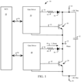
- FIG. 1 shows a schematic view of an embodiment 10 of a half bridge inverter system.
- the embodiment 10 includes a capacitor 12 as a DC Link decoupling supply or filtering element from the drain or collector of the high-side transistor 18, to the source or emitter of the low-side transistor 20 and may be charged to a DC BUS voltage (e.g., the voltage between the upper supply 14 and the lower supply 16).
- the upper supply is a Direct Current (DC) bus, having a voltage greater than a voltage of the lower supply 16.
- the capacitive load 12 may be charged or discharged with a cascode arrangement of a high-side transistor 18 connected in series with a low-side transistor 20.
- the high-side transistor 18 is connected to the low-side transistor 20 at a phase node 22.
- the high-side transistor 18 is driven by a gate driver 30, which generates gate control signals on node 32.
- the gate driver 30 also is capable of generating a calibrated current, (not shown), on a node 34, which may be connected to a resistor 36 in series with an anode of a voltage blocking diode 38.
- a cathode of the diode 38 connects to the source/drain of the high-side transistor (e.g., a power device) 18.
- the low-side transistor 20 is driven by a gate driver 40, which generates gate control signals on node 42.
- the gate driver 30 also generates a calibrated current (e.g., a desaturation current) 44 on a node 46, which further connects to a resistor 48 in series with an anode of a diode 50.
- a cathode of the diode 50 connects to the drain or collector of the low-side device 20.
- the resistors 36 and 48 are removed.
- the diodes 38 and 50 protect the low voltage circuitry of the gate driver or similar IC from the high potentials seen at the Drain/Collector of the power devices when they are off.
- the calibrated currents sourced from the respective gate drivers 30 and 40 are chosen to minimize the effect of parasitic leakage currents and to shorten the time required to determine the threshold voltages of the respective high-side transistor 18 and/or low-side transistor 20.
- the threshold voltage of the high-side transistor 18 is determined, while the low-side transistor 20 remains in an off state. In another embodiment, the threshold voltage of the low-side transistor 20 is determined, while the high-side transistor 18 remains in an off state.
- the threshold voltages of both the high-side transistor 18 and the low-side transistor 20 are determined individually.
- the methods described herein for measuring gate voltages with a calibrated current rely upon one of the two transistors 18 and 20 to be in the off state, thus also ensuring the half-bridge is in a "safely-off" condition.
- the gate driver 30 produces a voltage (GND or negative) with respect to source or emitter of the high-side transistor 18 sufficient to deactivate the high-side transistor 18.
- the gate driver 40 supplies a calibrated current 44 to the collector or drain of the low-side transistor 20, at the phase node 22, which causes the voltage across the low-side transistor 20 to rise. As the high-side transistor 18 and the low-side transistor 20 remain in a high-impedance state while both transistors 18 and 20 are deactivated, this voltage at node 22 will be maintained as long as the current 44 continues to be sourced.
- the gate driver 40 provides voltage pulses to the node 42 with sequentially increasing voltage until the low-side transistor 20 activates.
- the gate driver 40 provides a series of increasing voltage levels as a step function. Activation of the low-side transistor 20 may be determined by monitoring the collector to emitter, or drain to source voltage of the low-side transistor 20 at the phase node 22 with a comparator circuit of the gate driver 40.
- the minimum pulsed voltage required to activate the low-side transistor 20 e.g. Vgs
- Ids current e.g., the calibrated current 44
- Each gate driver 30 and 40 communicates with a Micro Control Unit (MCU) 52 or similar computing device, over a respective communication bus 54 and 56.
- MCU Micro Control Unit
- the MCU 52 operates in lower voltage domain than the remaining circuitry of the embodiment 10.
- the determined minimum pulsed voltage required to active the low-side transistor 20 is communicated to the MCU 52, and may or may not be normalized by the gate driver with respect to a measured temperature to determine the threshold voltage of the low-side transistor 20, (or the high-side transistor 18 in another embodiment).
- the MCU will take the raw voltage threshold measurements from the gate driver and will normalize with respect to system level temperature, or device level temperature.
- the measured temperature is one of a system level temperature, an ambient temperature, a coolant temperature of a heat sinking device thermally coupled to the embodiment 10 or device temperature (e.g., measured with an integrated diode of an integrated circuit comprising either the low-side transistor 20 or high-side transistor 18).
- the normalized threshold voltage is stored by the MCU 52 in a memory device.
- the measured temperature and the measured minimum pulsed voltage or stepped voltage are both stored in the memory device.
- the normalized threshold voltage of the low-side transistor 20 is determined repeatedly over time.
- the MCU 52 compares two or more stored and normalized threshold voltages to a present or recent determination of the threshold voltage to determine a threshold voltage change.
- a change in the threshold voltage exceeding a voltage limit may indicate that the transistor being measured has aged beyond an acceptable design or reliability limit.
- the MCU 52 may then further respond to the indication of aging by notifying a system user of the embodiment 10, or deactivating circuitry including or related to the aged component.
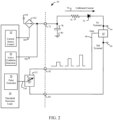
- FIG. 2 shows a schematic view of an embodiment 60 of a circuit for in situ determination of a threshold voltage of a device 62.
- the device 62 is an IGBT, a Silicon Carbide IGFET, a Gallium Nitride IGFET, a Gallium Arsenide MOSFET or any transistor having an insulated gate terminal wherein the device variably conducts a current in response to a gate voltage exceeding a threshold voltage of the device.
- the device 62 is configured to conduct current between a first terminal 64 and a second terminal 66, in response to a gate voltage in excess of a threshold voltage of the device 62 being applied to a gate terminal 68.
- a calibrated current 70 is sourced from a terminal 72, through a resistor 74 connected in series with a diode 76.
- a cathode of the diode 76 connects to the first terminal 64.
- the terminal 72 further connects to a charging capacitor 78 connected to a ground 80.
- the calibrated current 70 biases the first terminal 64 to a voltage above a voltage limit, and the voltage on the gate terminal 68 is less than the threshold voltage of the device 62, thereby putting the device 62 in an "inactive" condition.
- the device 62 enters an "active" condition, and discharges the first terminal 64 to a level below the voltage limit.
- the gate terminal of the device 62 is insulated so that minimal current conduction occurs between the gate terminal 68 and the second terminal 66. Accordingly, when the device 62 enters the active condition, the current flowing between the first terminal 64 and the second terminal 66 is the same as the calibrated current 70.
- the gate terminal 68 receives a series of pulses or voltage steps with sequentially increasing voltages at a terminal 82.
- the embodiment 60 further includes a threshold detection logic circuit 90.
- the threshold detection logic circuit 90 includes a current source control circuit 92, an active condition detection circuit 94 and a pulse generator circuit 96.
- the current source control circuit 92 generates a control signal 100 to control a current source 102, to generate the calibrated current 70 from a voltage source 104.
- the voltage source 104 is connected to the upper supply 14 of FIG. 1 .
- the active condition detection circuit 94 monitors a voltage on a node 106 to determine a voltage change on the first terminal 64.
- the pulse generator circuit 96 generates a control signal 110, which controls a variable voltage source 112 to generate a series of pulses with sequentially increasing voltages on the terminal 82.
- the pulse generator circuit 96 is replaced with a stepped function generator.
- the circuitry included in the threshold detection logic circuit 90 the current source 102 and the variable voltage source 112 is included in the gate driver 30 or the gate driver 40 of FIG. 1 .
- FIG. 3 shows a schematic view of an embodiment 120 of a variable voltage pulse generator circuit, performing a similar function to the pulse generator 96 and variable voltage source 112 of FIG. 2 .
- the embodiment 120 includes a Digital to Analog Converter (DAC) (configured to receive a sequential series of digital values on an input bus 124 and to generate an equivalent analog value on a node 126.
- An amplifier 130 is arranged in a voltage follower configuration to provide the analog value from the node 126 on the terminal 82.
- the amplifier 130 is enabled with an enable signal (En) on the node 132.
- a pull-down transistor 134 is enabled with an inverted enable signal (Enb) on node 136.
- the signal Enb on node 136 is formed by inverting the signal on the node 132 and is active during state transitions on the digital input bus 124, thereby forming a series of voltage pulses on the terminal 82.
- a duty cycle of the generated voltage pulses is minimized to provide protection against excessive current consumption in the event that the (opposing low-side or high-side transistor is shorted due to a fault) phase node 22 of FIG. 1 , or the first terminal 64 of FIG. 2 is shorted to ground due to a fault.
- the duty cycle may be varied by adjusting an ON time, a frequency of the pulse, or both.
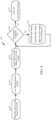
- FIG. 4 shows an embodiment 140 of a method for in situ threshold voltage determination of a device.
- the high-side switch (e.g., a transistor) 18 and the low-side switch (e.g., a transistor) 20 are turned off.
- voltage detection circuit e.g., a low-side desaturation verifier in one embodiment
- a minimum gate voltage is applied to the low-side switch 20.
- the minimum gate voltage is determined by a value less than the minimum anticipated threshold voltage of the low-side transistor 20 taking into consideration process, voltage and temperature variations.
- the desaturation comparator or any generalized voltage comparator is checked for a zero condition.
- the active condition detection circuit 94 of FIG. 2 verifies that the node 106 has been discharged below the voltage limit to indicate that the low-side transistor 20 is "ON". If the condition at 148 is true, the applied voltage on the low-side switch 20 exceeds its threshold voltage and the applied voltage is then normalized with a temperature and the determined threshold voltage of the low-side switch 20 is stored. Otherwise, the gate voltage is turned off, incremented and reapplied at 150.
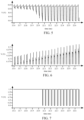
- FIG. 5, FIG. 6 and FIG. 7 with reference to FIG. 1 shows the voltages, across the transistor being tested, the gate pulse voltage applied to node 42 and a comparator output (e.g., an output of the active condition detection circuit 94) respectively, in accordance with the embodiment 10.
- a comparator output e.g., an output of the active condition detection circuit 94
- FIG. 5 the voltage on the phase node 22 varies due to parasitic coupling but does not drop below a voltage limit (indicating that the low-side transistor 20 has been activated), until after 22.0ms.
- FIG. 6 shows sequentially increasing pulse voltages
- FIG. 6 shows sequentially increasing pulse voltages
- the threshold voltage measurement can be stored and communicated, then the measurement sequence exited.
- FIG. 8 shows an example embodiment 160 of a method for in situ threshold voltage determination of a device.
- a current 70 is sourced to a first terminal 64 of a device 62.
- an insulated gate terminal 68 of the device 62 is driven with a series of gate levels with different voltage values in response to an inactive condition (e.g., a voltage level on node 106 transitioning past a voltage limit).
- an inactive condition e.g., a voltage level on node 106 transitioning past a voltage limit.
- a device voltage is measured between a first terminal 64 and a second terminal 66 of the device 62.
- the respective gate voltage is stored in response to an active condition, for example in a memory device in the MCU 52 of FIG. 1 or coupled thereto.
- a threshold voltage of the device 62 is estimated.
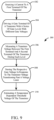
- FIG. 9 shows an example embodiment 180 of a method for in situ threshold voltage determination of a transistor.
- a current 70 is sourced to a first terminal 64 of a transistor 62.
- a gate terminal 68 of the transistor 62 is driven with a series of gate levels with different gate voltages.
- a transistor voltage is measured between a first terminal 64 and a second terminal 66 of the transistor 62 during each level.
- the respective gate voltage is stored in response to the transistor voltage transitioning past a voltage limit (e.g., as measured by the active condition detection circuit 94).
- a temperature dependent threshold voltage of the transistor 62 is estimated.
- FIG. 10 shows an example embodiment 200 of a method for in situ aging determination of a half bridge inverter.
- a current 44 e.g., a desaturation current
- a gate terminal 42 of a first transistor 20 of the half bridge inverter 10 is driven with a series of gate levels with sequentially increasing gate voltages.
- a transistor voltage is measured between the first terminal 22 and a second terminal 16 of the half bridge inverter 10 during each gate level.
- the respective gate voltage is stored in response to the transistor voltage transitioning past a voltage limit (e.g., as measured by the active condition detection circuit 94 within the gate driver 40).
- a temperature measurement is performed (e.g., of an ambient temperature, a coolant temperature of a heat sink or a device temperature of the low-side transistor 20).
- a temperature dependent threshold voltage of the transistor 20 is estimated by correlating previous thresholds at the same temperature, or in another embodiment the threshold at temperature can be normalized to a previous data taken at different temperatures.
- a method for in situ threshold voltage determination of a device comprises sourcing a current to a first terminal of the device.
- An insulated gate terminal of the device is driven with a plurality of gate levels in response to a device voltage indicating an inactive condition of the device, wherein each gate level comprises a respective gate voltage being different than the respective gate voltage of a temporally adjacent and preceding gate level.
- the device voltage is measured between the first terminal and a second terminal of the device.
- the device is configured to variably conduct a device current thereinbetween in response to the respective gate voltage exceeding a threshold voltage of the device.
- the respective gate voltage is stored in response to the device voltage indicating an active condition of the device.
- a change in the threshold voltage of the device is estimated by comparing the stored gate voltage with a previously stored gate voltage.
- a temperature difference between a first measured temperature of the stored gate voltage and a second measured temperature of the previously stored gate voltage is less than a temperature threshold.
- the plurality of gate levels comprises a step function.
- the plurality of gate levels comprises gate pulses.
- a duty cycle of each of the plurality of gate pulses is limited.
- the respective gate voltage of each gate level increases from the respective gate voltage of the temporally adjacent and preceding gate level.
- the change in the threshold voltage is compared to a voltage limit to determine an incipient fault condition of the device.
- the first terminal is charged to a precharged voltage with the current and the inactive condition is determined in response to the device voltage exceeding a voltage limit.
- a method for in situ threshold voltage determination of a transistor comprises sourcing a current to a first terminal of the transistor.
- a gate terminal of the transistor is driven with a plurality of gate levels. Each gate level comprises one of a plurality of different gate voltages.
- a transistor voltage is measured between the first terminal and a second terminal of the transistor during each gate level.
- the respective gate voltage is stored in response to the transistor voltage transitioning past a voltage limit.
- a temperature dependent threshold voltage of the transistor is estimated for a first measured temperature measured during the storing of the stored gate voltage from a previously stored gate voltage and a second measured temperature.
- the transistor comprises an Insulated Gate Bipolar Transistor.
- the transistor comprises a Field Effect Transistor.
- the plurality of gate levels comprises a step function. Each of the plurality of gate levels comprises a gate pulse and the sequentially increasing gate voltage of each gate pulse is determined by incrementing an analog voltage with a Digital to Analog Converter to modulate an output of an amplifier, wherein the output generates each gate pulse.
- the transistor comprises a low-side transistor of a half-bridge inverter.
- the transistor comprises a high-side transistor of a half-bridge inverter.
- a method for in situ aging determination of a half bridge inverter comprises sourcing a current to a first terminal of a first transistor of the half bridge inverter.
- a gate terminal of the first transistor is driven with a plurality of gate levels. Each gate level comprises one of a plurality of sequentially increasing gate voltages.
- the half bridge inverter comprises the first transistor and a second transistor, wherein the first transistor connects between the first terminal and a second terminal, and a second transistor connects in series with the first transistor.
- a transistor voltage is measured between the first terminal and the second terminal during each gate level.
- the respective gate voltage is stored in response to the transistor voltage transitioning past a voltage limit.
- a temperature is measured to generate a temperature measurement.
- a temperature dependent threshold voltage of the first transistor is estimated for a first measured temperature measured during the storing of the stored gate voltage from a previously stored gate voltage and a second measured temperature.
- Alternative embodiments of the method for in situ aging determination of a half bridge inverter include one of the following features, or any combination thereof.
- a change in the temperature dependent threshold voltage of the first transistor is estimated between the stored gate voltage and the previously stored gate voltage normalized for a difference between the first measured temperature and the second measured temperature and performing a system level action in response thereto.
- the current value of the current is calibrated to enable the estimation of the threshold voltage to nullify changes to the threshold voltage due to a time-dependent variation in the current.
- the temperature varies in proportion to a transistor temperature of the first transistor.
- the second transistor is turned off prior to driving the gate terminal of the first transistor with the plurality of gate levels.
Landscapes
- Physics & Mathematics (AREA)
- General Physics & Mathematics (AREA)
- Engineering & Computer Science (AREA)
- Power Engineering (AREA)
- Microelectronics & Electronic Packaging (AREA)
- Testing Of Individual Semiconductor Devices (AREA)
Applications Claiming Priority (1)
| Application Number | Priority Date | Filing Date | Title |
|---|---|---|---|
| US17/571,699 US11821936B2 (en) | 2022-01-10 | 2022-01-10 | In situ threshold voltage determination of a semiconductor device |
Publications (2)
| Publication Number | Publication Date |
|---|---|
| EP4209791A1 true EP4209791A1 (de) | 2023-07-12 |
| EP4209791B1 EP4209791B1 (de) | 2025-11-05 |
Family
ID=84366912
Family Applications (1)
| Application Number | Title | Priority Date | Filing Date |
|---|---|---|---|
| EP22210616.3A Active EP4209791B1 (de) | 2022-01-10 | 2022-11-30 | In-situ-schwellenspannungsbestimmung einer halbleitervorrichtung |
Country Status (3)
| Country | Link |
|---|---|
| US (1) | US11821936B2 (de) |
| EP (1) | EP4209791B1 (de) |
| CN (1) | CN116413568A (de) |
Cited By (1)
| Publication number | Priority date | Publication date | Assignee | Title |
|---|---|---|---|---|
| TWI872683B (zh) * | 2023-08-17 | 2025-02-11 | 國立陽明交通大學 | 功率元件臨界電壓量測電路及其操作方法 |
Families Citing this family (1)
| Publication number | Priority date | Publication date | Assignee | Title |
|---|---|---|---|---|
| US12176802B2 (en) * | 2022-12-16 | 2024-12-24 | Bae Systems Controls Inc. | Multi-wire common mode choke for increasing common mode transient immunity and minimizing circulating current in paralleled power semiconductors |
Citations (4)
| Publication number | Priority date | Publication date | Assignee | Title |
|---|---|---|---|---|
| US5838164A (en) * | 1996-06-07 | 1998-11-17 | United Microelectronics Corporation | Method of measuring the threshold voltage of metal-oxide semiconductor field-effect transistors |
| US20180102773A1 (en) * | 2016-10-07 | 2018-04-12 | Texas Instruments Incorporated | Gate Driver with VGTH and VCESAT Measurement Capability for the State of Health Monitor |
| US20200343715A1 (en) * | 2019-04-23 | 2020-10-29 | Renesas Electronics Corporation | Drive device, power supply system, and method of testing drive device |
| US20200400738A1 (en) * | 2019-06-18 | 2020-12-24 | Board Of Regents, The University Of Texas System | Methods of monitoring conditions associated with aging of silicon carbide power mosfet devices in-situ, related circuits and computer program products |
Family Cites Families (9)
| Publication number | Priority date | Publication date | Assignee | Title |
|---|---|---|---|---|
| US5707035A (en) | 1994-08-31 | 1998-01-13 | Hoover Universal, Inc. | Vehicle seat adjuster |
| JP3885563B2 (ja) * | 2001-11-16 | 2007-02-21 | 日産自動車株式会社 | パワー半導体駆動回路 |
| JP4880867B2 (ja) * | 2002-04-10 | 2012-02-22 | セイコーインスツル株式会社 | 薄膜メモリ、アレイとその動作方法および製造方法 |
| KR100547040B1 (ko) * | 2003-12-31 | 2006-01-31 | 동부아남반도체 주식회사 | 십진 검색 방법을 이용한 문턱전압 측정방법 |
| US8912990B2 (en) * | 2008-04-21 | 2014-12-16 | Apple Inc. | Display having a transistor-degradation circuit |
| CN102473724B (zh) | 2009-08-18 | 2015-02-18 | 飞思卡尔半导体公司 | 晶体管功率开关器件及测量其特性的方法 |
| EP3109649B1 (de) | 2015-06-25 | 2019-08-07 | ABB Schweiz AG | Alterungsbestimmung eines leistungshalbleiterbauelements in elektrischem antriebssystem |
| US10288672B2 (en) | 2016-04-08 | 2019-05-14 | Nutech Ventures | Monitoring aging of power semiconductor devices based on case temperature |
| GB2559723A (en) * | 2016-11-29 | 2018-08-22 | Univ Surrey | Gas detector |
-
2022
- 2022-01-10 US US17/571,699 patent/US11821936B2/en active Active
- 2022-11-30 EP EP22210616.3A patent/EP4209791B1/de active Active
- 2022-12-01 CN CN202211531929.8A patent/CN116413568A/zh active Pending
Patent Citations (4)
| Publication number | Priority date | Publication date | Assignee | Title |
|---|---|---|---|---|
| US5838164A (en) * | 1996-06-07 | 1998-11-17 | United Microelectronics Corporation | Method of measuring the threshold voltage of metal-oxide semiconductor field-effect transistors |
| US20180102773A1 (en) * | 2016-10-07 | 2018-04-12 | Texas Instruments Incorporated | Gate Driver with VGTH and VCESAT Measurement Capability for the State of Health Monitor |
| US20200343715A1 (en) * | 2019-04-23 | 2020-10-29 | Renesas Electronics Corporation | Drive device, power supply system, and method of testing drive device |
| US20200400738A1 (en) * | 2019-06-18 | 2020-12-24 | Board Of Regents, The University Of Texas System | Methods of monitoring conditions associated with aging of silicon carbide power mosfet devices in-situ, related circuits and computer program products |
Non-Patent Citations (1)
| Title |
|---|
| IVAN BAHUN ET AL: "Real-Time Measurement of IGBT's Operating Temperature", JOURNAL FOR CONTROL, MEASUREMENT, ELECTRONICS, COMPUTING AND COMMUNICATIONS, vol. 52, no. 4, 31 December 2011 (2011-12-31), pages 295 - 305, XP055087873, ISSN: 0005-1144 * |
Cited By (2)
| Publication number | Priority date | Publication date | Assignee | Title |
|---|---|---|---|---|
| TWI872683B (zh) * | 2023-08-17 | 2025-02-11 | 國立陽明交通大學 | 功率元件臨界電壓量測電路及其操作方法 |
| US12523694B2 (en) | 2023-08-17 | 2026-01-13 | National Yang Ming Chiao Tung University | Power device threshold voltage measurement circuit and operation method thereof |
Also Published As
| Publication number | Publication date |
|---|---|
| US11821936B2 (en) | 2023-11-21 |
| EP4209791B1 (de) | 2025-11-05 |
| CN116413568A (zh) | 2023-07-11 |
| US20230221363A1 (en) | 2023-07-13 |
Similar Documents
| Publication | Publication Date | Title |
|---|---|---|
| US8044674B2 (en) | Semiconductor device with thermal fault detection | |
| CN109425816B (zh) | 测试mos功率开关 | |
| US10605854B2 (en) | Method for estimating power system health | |
| US10038436B2 (en) | Masking vd to vref after miller plateau and gate charge | |
| US9436193B2 (en) | Electric system comprising a load driving apparatus by auto-recovery mode, and method of operating the apparatus | |
| EP4209791A1 (de) | In-situ-schwellenspannungsbestimmung einer halbleitervorrichtung | |
| JP2003143833A (ja) | 半導体スイッチング素子のゲート駆動装置 | |
| US20130120030A1 (en) | Semiconductor device measuring voltage applied to semiconductor switch element | |
| JP5780145B2 (ja) | スイッチング素子駆動回路及びそれを備える駆動装置 | |
| US11528025B2 (en) | Driver circuit, system having a driver circuit, and calibration method | |
| US9857428B2 (en) | Monitoring device and monitoring method for a switching element | |
| US11879929B2 (en) | Method and device for automatically testing a switching member | |
| CN110247646A (zh) | 动态短路保护 | |
| US7839158B2 (en) | Method of detecting abnormality in burn-in apparatus | |
| CN115622372A (zh) | 应力测试模式的nmos功率晶体管和阻断电路的驱动器设备 | |
| KR101531018B1 (ko) | 전력반도체소자의 불량 예측 방법 | |
| JP2019017128A (ja) | 逆接続保護装置の状態検出回路 | |
| EP4468606A1 (de) | Temperaturkompensiertes überstromerkennungssystem | |
| US20230111154A1 (en) | Gate driver | |
| US20260118427A1 (en) | Power device system | |
| KR20180067130A (ko) | 전력 소자 모듈의 온도 센싱 장치 및 방법 | |
| US12235321B2 (en) | Method and device for monitoring a plurality of parallel-connected semiconductor switches | |
| US20250389787A1 (en) | Methods and apparatuses for de-energized circuit testing based on driver-induced electrical quantity | |
| US20260058647A1 (en) | Transistor module, driver for transistor module, corresponding system and method | |
| Li et al. | Detection and Identification of Switching Faults in Boost Converters Using an HSVG Sensing Circuit |
Legal Events
| Date | Code | Title | Description |
|---|---|---|---|
| PUAI | Public reference made under article 153(3) epc to a published international application that has entered the european phase |
Free format text: ORIGINAL CODE: 0009012 |
|
| STAA | Information on the status of an ep patent application or granted ep patent |
Free format text: STATUS: THE APPLICATION HAS BEEN PUBLISHED |
|
| AK | Designated contracting states |
Kind code of ref document: A1 Designated state(s): AL AT BE BG CH CY CZ DE DK EE ES FI FR GB GR HR HU IE IS IT LI LT LU LV MC ME MK MT NL NO PL PT RO RS SE SI SK SM TR |
|
| STAA | Information on the status of an ep patent application or granted ep patent |
Free format text: STATUS: REQUEST FOR EXAMINATION WAS MADE |
|
| 17P | Request for examination filed |
Effective date: 20240112 |
|
| RBV | Designated contracting states (corrected) |
Designated state(s): AL AT BE BG CH CY CZ DE DK EE ES FI FR GB GR HR HU IE IS IT LI LT LU LV MC ME MK MT NL NO PL PT RO RS SE SI SK SM TR |
|
| STAA | Information on the status of an ep patent application or granted ep patent |
Free format text: STATUS: EXAMINATION IS IN PROGRESS |
|
| 17Q | First examination report despatched |
Effective date: 20250603 |
|
| GRAP | Despatch of communication of intention to grant a patent |
Free format text: ORIGINAL CODE: EPIDOSNIGR1 |
|
| STAA | Information on the status of an ep patent application or granted ep patent |
Free format text: STATUS: GRANT OF PATENT IS INTENDED |
|
| INTG | Intention to grant announced |
Effective date: 20250731 |
|
| GRAS | Grant fee paid |
Free format text: ORIGINAL CODE: EPIDOSNIGR3 |
|
| GRAA | (expected) grant |
Free format text: ORIGINAL CODE: 0009210 |
|
| STAA | Information on the status of an ep patent application or granted ep patent |
Free format text: STATUS: THE PATENT HAS BEEN GRANTED |
|
| AK | Designated contracting states |
Kind code of ref document: B1 Designated state(s): AL AT BE BG CH CY CZ DE DK EE ES FI FR GB GR HR HU IE IS IT LI LT LU LV MC ME MK MT NL NO PL PT RO RS SE SI SK SM TR |
|
| REG | Reference to a national code |
Ref country code: CH Ref legal event code: F10 Free format text: ST27 STATUS EVENT CODE: U-0-0-F10-F00 (AS PROVIDED BY THE NATIONAL OFFICE) Effective date: 20251105 Ref country code: GB Ref legal event code: FG4D |
|
| REG | Reference to a national code |
Ref country code: DE Ref legal event code: R096 Ref document number: 602022024343 Country of ref document: DE |
|
| REG | Reference to a national code |
Ref country code: IE Ref legal event code: FG4D |
|
| PGFP | Annual fee paid to national office [announced via postgrant information from national office to epo] |
Ref country code: DE Payment date: 20251126 Year of fee payment: 4 |
|
| REG | Reference to a national code |
Ref country code: NL Ref legal event code: MP Effective date: 20251105 |
|
| PG25 | Lapsed in a contracting state [announced via postgrant information from national office to epo] |
Ref country code: ES Free format text: LAPSE BECAUSE OF FAILURE TO SUBMIT A TRANSLATION OF THE DESCRIPTION OR TO PAY THE FEE WITHIN THE PRESCRIBED TIME-LIMIT Effective date: 20251105 |
|
| REG | Reference to a national code |
Ref country code: LT Ref legal event code: MG9D |
|
| PG25 | Lapsed in a contracting state [announced via postgrant information from national office to epo] |
Ref country code: NO Free format text: LAPSE BECAUSE OF FAILURE TO SUBMIT A TRANSLATION OF THE DESCRIPTION OR TO PAY THE FEE WITHIN THE PRESCRIBED TIME-LIMIT Effective date: 20260205 |
|
| PG25 | Lapsed in a contracting state [announced via postgrant information from national office to epo] |
Ref country code: FI Free format text: LAPSE BECAUSE OF FAILURE TO SUBMIT A TRANSLATION OF THE DESCRIPTION OR TO PAY THE FEE WITHIN THE PRESCRIBED TIME-LIMIT Effective date: 20251105 Ref country code: AT Free format text: LAPSE BECAUSE OF FAILURE TO SUBMIT A TRANSLATION OF THE DESCRIPTION OR TO PAY THE FEE WITHIN THE PRESCRIBED TIME-LIMIT Effective date: 20251105 Ref country code: HR Free format text: LAPSE BECAUSE OF FAILURE TO SUBMIT A TRANSLATION OF THE DESCRIPTION OR TO PAY THE FEE WITHIN THE PRESCRIBED TIME-LIMIT Effective date: 20251105 |
|
| REG | Reference to a national code |
Ref country code: AT Ref legal event code: MK05 Ref document number: 1854895 Country of ref document: AT Kind code of ref document: T Effective date: 20251105 |
|
| PG25 | Lapsed in a contracting state [announced via postgrant information from national office to epo] |
Ref country code: NL Free format text: LAPSE BECAUSE OF FAILURE TO SUBMIT A TRANSLATION OF THE DESCRIPTION OR TO PAY THE FEE WITHIN THE PRESCRIBED TIME-LIMIT Effective date: 20251105 |
|
| PG25 | Lapsed in a contracting state [announced via postgrant information from national office to epo] |
Ref country code: RS Free format text: LAPSE BECAUSE OF FAILURE TO SUBMIT A TRANSLATION OF THE DESCRIPTION OR TO PAY THE FEE WITHIN THE PRESCRIBED TIME-LIMIT Effective date: 20260205 |
|
| PG25 | Lapsed in a contracting state [announced via postgrant information from national office to epo] |
Ref country code: IS Free format text: LAPSE BECAUSE OF FAILURE TO SUBMIT A TRANSLATION OF THE DESCRIPTION OR TO PAY THE FEE WITHIN THE PRESCRIBED TIME-LIMIT Effective date: 20260305 |
|
| PG25 | Lapsed in a contracting state [announced via postgrant information from national office to epo] |
Ref country code: PT Free format text: LAPSE BECAUSE OF FAILURE TO SUBMIT A TRANSLATION OF THE DESCRIPTION OR TO PAY THE FEE WITHIN THE PRESCRIBED TIME-LIMIT Effective date: 20260305 |
|
| PG25 | Lapsed in a contracting state [announced via postgrant information from national office to epo] |
Ref country code: PL Free format text: LAPSE BECAUSE OF FAILURE TO SUBMIT A TRANSLATION OF THE DESCRIPTION OR TO PAY THE FEE WITHIN THE PRESCRIBED TIME-LIMIT Effective date: 20251105 |
|
| PG25 | Lapsed in a contracting state [announced via postgrant information from national office to epo] |
Ref country code: LV Free format text: LAPSE BECAUSE OF FAILURE TO SUBMIT A TRANSLATION OF THE DESCRIPTION OR TO PAY THE FEE WITHIN THE PRESCRIBED TIME-LIMIT Effective date: 20251105 |