EP4210077A1 - Composant électronique et dispositif électronique - Google Patents
Composant électronique et dispositif électronique Download PDFInfo
- Publication number
- EP4210077A1 EP4210077A1 EP21868332.4A EP21868332A EP4210077A1 EP 4210077 A1 EP4210077 A1 EP 4210077A1 EP 21868332 A EP21868332 A EP 21868332A EP 4210077 A1 EP4210077 A1 EP 4210077A1
- Authority
- EP
- European Patent Office
- Prior art keywords
- electronic component
- cushioning
- pad
- disposed
- stress
- Prior art date
- Legal status (The legal status is an assumption and is not a legal conclusion. Google has not performed a legal analysis and makes no representation as to the accuracy of the status listed.)
- Pending
Links
Images


Classifications
-
- H—ELECTRICITY
- H05—ELECTRIC TECHNIQUES NOT OTHERWISE PROVIDED FOR
- H05K—PRINTED CIRCUITS; CASINGS OR CONSTRUCTIONAL DETAILS OF ELECTRIC APPARATUS; MANUFACTURE OF ASSEMBLAGES OF ELECTRICAL COMPONENTS
- H05K1/00—Printed circuits
- H05K1/18—Printed circuits structurally associated with non-printed electric components
- H05K1/181—Printed circuits structurally associated with non-printed electric components associated with surface mounted components
-
- H—ELECTRICITY
- H01—ELECTRIC ELEMENTS
- H01G—CAPACITORS; CAPACITORS, RECTIFIERS, DETECTORS, SWITCHING DEVICES, LIGHT-SENSITIVE OR TEMPERATURE-SENSITIVE DEVICES OF THE ELECTROLYTIC TYPE
- H01G2/00—Details of capacitors not covered by a single one of groups H01G4/00-H01G11/00
- H01G2/02—Mountings
- H01G2/06—Mountings specially adapted for mounting on a printed-circuit support
-
- H—ELECTRICITY
- H01—ELECTRIC ELEMENTS
- H01G—CAPACITORS; CAPACITORS, RECTIFIERS, DETECTORS, SWITCHING DEVICES, LIGHT-SENSITIVE OR TEMPERATURE-SENSITIVE DEVICES OF THE ELECTROLYTIC TYPE
- H01G4/00—Fixed capacitors; Processes of their manufacture
- H01G4/002—Details
- H01G4/224—Housing; Encapsulation
-
- H—ELECTRICITY
- H01—ELECTRIC ELEMENTS
- H01G—CAPACITORS; CAPACITORS, RECTIFIERS, DETECTORS, SWITCHING DEVICES, LIGHT-SENSITIVE OR TEMPERATURE-SENSITIVE DEVICES OF THE ELECTROLYTIC TYPE
- H01G4/00—Fixed capacitors; Processes of their manufacture
- H01G4/002—Details
- H01G4/228—Terminals
- H01G4/232—Terminals electrically connecting two or more layers of a stacked or rolled capacitor
-
- H—ELECTRICITY
- H01—ELECTRIC ELEMENTS
- H01G—CAPACITORS; CAPACITORS, RECTIFIERS, DETECTORS, SWITCHING DEVICES, LIGHT-SENSITIVE OR TEMPERATURE-SENSITIVE DEVICES OF THE ELECTROLYTIC TYPE
- H01G4/00—Fixed capacitors; Processes of their manufacture
- H01G4/40—Structural combinations of fixed capacitors with other electric elements, the structure mainly consisting of a capacitor, e.g. RC combinations
-
- H—ELECTRICITY
- H05—ELECTRIC TECHNIQUES NOT OTHERWISE PROVIDED FOR
- H05K—PRINTED CIRCUITS; CASINGS OR CONSTRUCTIONAL DETAILS OF ELECTRIC APPARATUS; MANUFACTURE OF ASSEMBLAGES OF ELECTRICAL COMPONENTS
- H05K1/00—Printed circuits
- H05K1/02—Details
- H05K1/11—Printed elements for providing electric connections to or between printed circuits
- H05K1/111—Pads for surface mounting, e.g. lay-out
-
- H—ELECTRICITY
- H05—ELECTRIC TECHNIQUES NOT OTHERWISE PROVIDED FOR
- H05K—PRINTED CIRCUITS; CASINGS OR CONSTRUCTIONAL DETAILS OF ELECTRIC APPARATUS; MANUFACTURE OF ASSEMBLAGES OF ELECTRICAL COMPONENTS
- H05K3/00—Apparatus or processes for manufacturing printed circuits
- H05K3/30—Assembling printed circuits with electric components, e.g. with resistors
- H05K3/32—Assembling printed circuits with electric components, e.g. with resistors electrically connecting electric components or wires to printed circuits
- H05K3/34—Assembling printed circuits with electric components, e.g. with resistors electrically connecting electric components or wires to printed circuits by soldering
- H05K3/341—Surface mounted components
- H05K3/3431—Leadless components
-
- H—ELECTRICITY
- H05—ELECTRIC TECHNIQUES NOT OTHERWISE PROVIDED FOR
- H05K—PRINTED CIRCUITS; CASINGS OR CONSTRUCTIONAL DETAILS OF ELECTRIC APPARATUS; MANUFACTURE OF ASSEMBLAGES OF ELECTRICAL COMPONENTS
- H05K3/00—Apparatus or processes for manufacturing printed circuits
- H05K3/30—Assembling printed circuits with electric components, e.g. with resistors
- H05K3/32—Assembling printed circuits with electric components, e.g. with resistors electrically connecting electric components or wires to printed circuits
- H05K3/34—Assembling printed circuits with electric components, e.g. with resistors electrically connecting electric components or wires to printed circuits by soldering
- H05K3/3452—Solder masks
-
- H—ELECTRICITY
- H01—ELECTRIC ELEMENTS
- H01G—CAPACITORS; CAPACITORS, RECTIFIERS, DETECTORS, SWITCHING DEVICES, LIGHT-SENSITIVE OR TEMPERATURE-SENSITIVE DEVICES OF THE ELECTROLYTIC TYPE
- H01G2/00—Details of capacitors not covered by a single one of groups H01G4/00-H01G11/00
- H01G2/02—Mountings
- H01G2/06—Mountings specially adapted for mounting on a printed-circuit support
- H01G2/065—Mountings specially adapted for mounting on a printed-circuit support for surface mounting, e.g. chip capacitors
-
- H—ELECTRICITY
- H01—ELECTRIC ELEMENTS
- H01G—CAPACITORS; CAPACITORS, RECTIFIERS, DETECTORS, SWITCHING DEVICES, LIGHT-SENSITIVE OR TEMPERATURE-SENSITIVE DEVICES OF THE ELECTROLYTIC TYPE
- H01G4/00—Fixed capacitors; Processes of their manufacture
- H01G4/002—Details
- H01G4/018—Dielectrics
- H01G4/06—Solid dielectrics
- H01G4/08—Inorganic dielectrics
- H01G4/12—Ceramic dielectrics
-
- H—ELECTRICITY
- H01—ELECTRIC ELEMENTS
- H01G—CAPACITORS; CAPACITORS, RECTIFIERS, DETECTORS, SWITCHING DEVICES, LIGHT-SENSITIVE OR TEMPERATURE-SENSITIVE DEVICES OF THE ELECTROLYTIC TYPE
- H01G4/00—Fixed capacitors; Processes of their manufacture
- H01G4/30—Stacked capacitors
-
- H—ELECTRICITY
- H05—ELECTRIC TECHNIQUES NOT OTHERWISE PROVIDED FOR
- H05K—PRINTED CIRCUITS; CASINGS OR CONSTRUCTIONAL DETAILS OF ELECTRIC APPARATUS; MANUFACTURE OF ASSEMBLAGES OF ELECTRICAL COMPONENTS
- H05K2201/00—Indexing scheme relating to printed circuits covered by H05K1/00
- H05K2201/09—Shape and layout
- H05K2201/09209—Shape and layout details of conductors
- H05K2201/09654—Shape and layout details of conductors covering at least two types of conductors provided for in H05K2201/09218 - H05K2201/095
- H05K2201/09663—Divided layout, i.e. conductors divided in two or more parts
-
- H—ELECTRICITY
- H05—ELECTRIC TECHNIQUES NOT OTHERWISE PROVIDED FOR
- H05K—PRINTED CIRCUITS; CASINGS OR CONSTRUCTIONAL DETAILS OF ELECTRIC APPARATUS; MANUFACTURE OF ASSEMBLAGES OF ELECTRICAL COMPONENTS
- H05K2201/00—Indexing scheme relating to printed circuits covered by H05K1/00
- H05K2201/09—Shape and layout
- H05K2201/09818—Shape or layout details not covered by a single group of H05K2201/09009 - H05K2201/09809
- H05K2201/099—Coating over pads, e.g. solder resist partly over pads
-
- H—ELECTRICITY
- H05—ELECTRIC TECHNIQUES NOT OTHERWISE PROVIDED FOR
- H05K—PRINTED CIRCUITS; CASINGS OR CONSTRUCTIONAL DETAILS OF ELECTRIC APPARATUS; MANUFACTURE OF ASSEMBLAGES OF ELECTRICAL COMPONENTS
- H05K2201/00—Indexing scheme relating to printed circuits covered by H05K1/00
- H05K2201/10—Details of components or other objects attached to or integrated in a printed circuit board
- H05K2201/10007—Types of components
- H05K2201/10015—Non-printed capacitor
-
- H—ELECTRICITY
- H05—ELECTRIC TECHNIQUES NOT OTHERWISE PROVIDED FOR
- H05K—PRINTED CIRCUITS; CASINGS OR CONSTRUCTIONAL DETAILS OF ELECTRIC APPARATUS; MANUFACTURE OF ASSEMBLAGES OF ELECTRICAL COMPONENTS
- H05K2201/00—Indexing scheme relating to printed circuits covered by H05K1/00
- H05K2201/10—Details of components or other objects attached to or integrated in a printed circuit board
- H05K2201/10613—Details of electrical connections of non-printed components, e.g. special leads
- H05K2201/10621—Components characterised by their electrical contacts
- H05K2201/10636—Leadless chip, e.g. chip capacitor or resistor
-
- H—ELECTRICITY
- H05—ELECTRIC TECHNIQUES NOT OTHERWISE PROVIDED FOR
- H05K—PRINTED CIRCUITS; CASINGS OR CONSTRUCTIONAL DETAILS OF ELECTRIC APPARATUS; MANUFACTURE OF ASSEMBLAGES OF ELECTRICAL COMPONENTS
- H05K2201/00—Indexing scheme relating to printed circuits covered by H05K1/00
- H05K2201/10—Details of components or other objects attached to or integrated in a printed circuit board
- H05K2201/10613—Details of electrical connections of non-printed components, e.g. special leads
- H05K2201/10954—Other details of electrical connections
- H05K2201/10984—Component carrying a connection agent, e.g. solder, adhesive
Definitions
- Embodiments of this application relate to the field of capacitor technologies, and in particular, to an electronic component and an electronic device.
- Multi-layer Ceramic Capacitors are widely used in electronic products.
- PCB printed circuit Board
- the electronic component includes a ceramic medium.
- cracking occurs.
- an internal circuit of an electronic product is short-circuited or disconnected. Sensitivity of the electronic product is affected, or the electronic product fails.
- Embodiments of this application provide an electronic component and an electronic device and resolve a problem of poor reliability of the electronic component.
- an electronic component is provided.
- the electronic component is disposed on a PCB.
- the electronic component includes an electronic component body.
- the electronic component body is soldered to the PCB by using a connecting component.
- the connecting component is provided with at least one cushioning structure.
- the connecting component is provided with the at least one cushioning structure, so that stress may be released at a position of the cushioning structure when the electronic component is subjected to mechanical stress. Stress on the electronic component body is reduced, and the electronic component body is prevented from cracking under the stress, thereby improving reliability of the electronic component.
- the cushioning structure is in a rectangular, circular, or irregular shape.
- the cushioning structure and the connecting component form a "rectangular-ambulatory-plane" structure. Therefore, the stress may be released at the cushioning structure.
- a shape of the cushioning structure includes any one of the following: a straight line shape, a curve shape, and a zigzag line shape. Therefore, the shape of the cushioning structure is more flexible.
- the connecting component includes a first side and a second side that are opposite to each other.
- the cushioning structure passes through the first side and the second side of the connecting component. Therefore, the cushioning structure may divide a force-bearing surface of the connecting component into two independent parts, so that the stress cannot be continuously transferred to the electronic component body. Reliability of the electronic component is improved.
- the cushioning structures are disposed in a cross shape.
- the two cushioning structures respectively pass through two opposite sides of the connecting component. Therefore, the cushioning structures may further divide the force-bearing surface of the connecting component into four independent parts, so that the stress cannot be continuously transferred to the electronic component body. Reliability of the electronic component is improved.
- the connecting component includes a pad.
- the pad is provided with at least one cushioning structure. Therefore, the connecting component has a simple structure and is easy to assemble.
- the connecting component includes a pad and a connecting material.
- the connecting material is located between the pad and the electronic component body.
- the connecting material is provided with at least one cushioning structure. In this way, connection stability is improved by providing the connecting material. Moreover, it is easier to operate because an original mechanism of the pad does not need to be changed.
- the connecting material includes at least one of solder and electrically conductive adhesive.
- the electronic component further includes termination electrodes covering two ends of the electronic component body.
- the termination electrodes are soldered to the circuit board by using the connecting material. Therefore, the electronic component body may be connected to the PCB more stably.
- the electronic component body is connected to the termination electrodes by using electrically conductive resin or the electrically conductive adhesive.
- the elastomeric conductive material may better absorb the mechanical stress applied to the electronic component body.
- the electronic component body is prevented from cracking under the stress, and reliability of the electronic component is improved.
- the cushioning structure includes at least one of the following: an opening disposed on the connecting component, and a cushioning member disposed between the connecting component and the electronic component body.
- stress may be released by using the opening or the cushioning member. Stress on the electronic component body is reduced, and the electronic component body is prevented from cracking under the stress. Reliability of the electronic component is improved.
- the cushioning member is a solder mask layer.
- the electronic component body is disconnected from the PCB at a position of the solder mask layer by providing the solder mask layer.
- the force-bearing surface is divided, and stress cannot be continuously transferred to the electronic component body. Reliability of the electronic component is improved.
- an electronic device includes a PCB and the foregoing electronic component.
- the electronic component is disposed on the PCB. Therefore, the foregoing electronic component has a same technical effect as the electronic component provided in the foregoing embodiment, and details are not described herein again.
- position terms such as “top” and “bottom” are defined relative to positions of components in the accompanying drawings. It should be understood that these position terms are relative concepts used for relative description and clarification, and may correspondingly change based on changes in the positions of the components in the accompanying drawings.
- An embodiment of this application provides an electronic device.
- the electronic device includes, for example, a mobile phone, a tablet computer, an in-vehicle computer, an intelligent wearable product, the Internet of Things (internet of things, IOT), and the like.
- IOT Internet of Things
- a specific form of the electronic device is not specially limited in the embodiment of this application.
- the electronic device includes a PCB, and an electronic component disposed on the PCB.
- the electronic component includes, for example, an electronic component whose body is prone to crack and fail, such as a multi-layer ceramic capacitor (Multi-layer Ceramic Capacitors, MLCC), an inductor, and a wafer level package (Wafer Level Package, WLP).
- MLCC Multi-layer Ceramic Capacitors
- WLP wafer Level Package
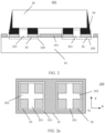
- FIG. 1a is a schematic diagram of a structure of a multi-layer ceramic capacitor. As shown in FIG. 1a , the multi-layer ceramic capacitor is disposed on a printed circuit board PCB 10.
- the multi-layer ceramic capacitor 001 includes a capacitor body 20.
- the capacitor body 20 is, for example, formed by multiple layers of ceramic having electrodes.
- the capacitor body 20 is connected to the PCB 10 by using, for example, a connecting component. In some embodiments, the connecting component may be a pad.
- FIG. 1b is a top view of a connecting component in FIG. 1a .
- the capacitor body 20 is soldered to pads 30 by using, for example, connecting materials 50, and the pads 30 are soldered to the PCB 10.
- the multi-layer ceramic capacitor 001 further includes termination electrodes.
- the termination electrodes are soldered to the circuit board by using the connecting materials 50.
- a material of the connecting material 50 may be a conductive material such as solder and electrically conductive adhesive.
- the solder includes, for example, a tin (Sn) alloy, a silver (Ag) alloy, and a copper (Cu) alloy.
- the termination electrode is in a shape of "]".
- the connecting material 50 is partially attached to an outer side of a part that is of a termination electrode and that is close to the circuit board, and is partially located between the capacitor body 20 and a pad 30. Two ends where the connecting material 50 is attached to the termination electrode are connected to roughly form a triangle on the capacitor body 20.
- a shape of the connecting material may be the triangle, or may be a trapezoid, a rectangle, or a part of a circle. Generally, a larger area covered by the connection parts indicates a better effect of preventing a short circuit.
- a solder mask layer 101 is disposed on a surface of the PCB 10. Openings are disposed on the solder mask layer 101.
- the pads 30 are disposed at the openings of the solder mask layer 101.
- a gap 1001 exists between the pad 30 and the solder mask layer 101.
- the solder mask layer 101 is not provided on surfaces of the pads 30.
- This design is non-solder mask defined (Non-Solder Mask Defined, NSMD) pads.
- a solder mask layer 101 is disposed on a surface of the PCB 10. Openings are disposed on the solder mask layer 101. The pads 30 are disposed at the openings of the solder mask layer 101. The solder mask layer 101 is provided around the pads 30. This design is solder mask defined (Solder Mask Defined) pads.
- a solder mask layer 101 is disposed on surfaces of some pads 30, and surfaces of some pads 30 are not provided with the solder mask layer 101.
- This design is NSMD/SMD hybrid pads. All these fall within the protection scope of this application.
- an embodiment of this application provides an improved multi-layer ceramic capacitor 001.
- the multi-layer ceramic capacitor 001 includes a capacitor body 20.
- the capacitor body 20 is soldered to a printed circuit board PCB 10 by using connecting components 100.
- the connecting component 100 is provided with at least one cushioning structure.
- a surface of the printed circuit board PCB 10 is provided with, for example, a solder mask layer 101.
- a material of the solder mask layer may be resin and have functions of moisture-proof, insulation, soldering-proof, and high temperature resistance.
- openings are disposed on the solder mask layer 101, and the connecting component 100 is disposed at the openings.
- the cushioning structure is not limited in this embodiment of this application.
- the cushioning structure includes a first opening 301 disposed on the connecting component 100.
- the cushioning structure includes a cushioning member 102 disposed between the connecting component 100 and the capacitor body 20.
- the cushioning members 102 may be an elastomeric component or a solder mask layer.
- the connecting component 100 is provided with at least one cushioning structure, so that stress may be released at a position of the cushioning structure when the multi-layer ceramic capacitor 001 is subjected to mechanical stress. Stress on the capacitor body 20 is reduced, and the capacitor body 20 is prevented from cracking under the stress. Reliability of the multi-layer ceramic capacitor 001 is improved.
- the position of the cushioning structure is not limited in this embodiment of this application.
- the cushioning structure may be disposed at a position where the multi-layer ceramic capacitor 001 is prone to crack. In some embodiments of this application, a middle position of the multi-layer ceramic capacitor 001 is prone to crack. Therefore, the cushioning structure may be disposed in the middle position of the capacitor body 20.
- the connecting component 100 includes a pad 30.
- the pad 30 is of a three-layer structure, including a capacitor body pad, a connecting material, and a PCB pad that are disposed in a stacked manner.
- One surface of the capacitor body 20 is soldered to the pad 30 by using a connecting material 50, and the pad 30 is soldered to the PCB 10.
- a shape of the connecting material 50 between the capacitor body 20 and the pad 30 matches that of the pad 30.
- the first opening 301 is disposed on the pad 30 as the cushioning structure.
- a shape of the cushioning structure is not limited in this embodiment of this application.
- the shape of the cushioning structure includes any one of the following: a straight line shape, a curve shape, and a zigzag line shape, for example, a" 1"-shape, "U”-shape, "V”-shape, "W”-shape, and "S”-shape.
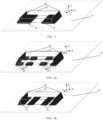
- the connecting component 100 includes a pad 30.
- the pad 30 is provided with two cushioning structures: a first opening 301 and a second opening 302.
- the first opening 301 and the second opening 302 are disposed in a cross shape.
- the first opening 301 is disposed horizontally, for example, in parallel to an X-axis direction, and extends from a first side of the pad 30 to a second side of the pad 30.
- the second opening 302 is disposed vertically, for example, in parallel to a Y-axis direction, and extends from a third side of the pad 30 to a fourth side of the pad 30.
- first opening 301 and the second opening 302 divide the pad 30 into four blocks.
- the connecting component 100 includes, for example, a first side and a second side that are opposite to each other.
- the cushioning structure passes through the first side and the second side.
- the first opening 301 parallel to the Y-axis direction is disposed on the pad 30.
- the pad 30 is divided into two blocks by the first opening 301 along the Y-axis direction.
- the width of the first opening 301 is, for example, one third of the length of a third side and a fourth side.
- the second opening 302 parallel to the X-axis direction is disposed on the pad 30.
- the pad 30 is divided into two blocks by the second opening 302 along the X-axis direction.
- the width of the second opening 302 is one third of the length of the first side and the second side.
- the cushioning structure is in a rectangular, circular, or irregular shape, and is disposed at a central position of the capacitor body 20. As shown in FIG. 2d , third openings 303 are disposed in the middle of the capacitor body 20, and a cross section of the capacitor body 20 is in a "rectangular-ambulatory-plane" shape.
- the openings are provided on the pads 30, so that in a conventional design of completely soldered pads 30, effectiveness of transferring deformation of the PCB 10 to the fragile capacitor body 20 is reduced. Therefore, stress and strain of the capacitor body 20 are reduced, and a ceramic cracking risk of the capacitor body 20 is thus reduced. Board-level application reliability of the multi-layer ceramic capacitor 001 is improved.
- a cushioning member 102 is disposed between the pad 30 and the capacitor body 20.
- An opening is disposed on a connecting material 50 between the pad 30 and the capacitor body 20.
- the cushioning member 102 is located in the opening, and a height of the connecting material 50 between the pad 30 and the capacitor body 20 is higher than that of the cushioning member 102.
- the connecting component 100 includes the pad 30.
- the pad 30 is provided with two cushioning structures: a first cushioning member 1021 and a second cushioning member 1022.
- the first cushioning member 1021 and the second cushioning member 1022 are disposed in a cross shape.
- the first cushioning member 1021 is disposed horizontally, for example, in parallel to an X-axis direction, and extends from the first side of the pad 30 to the second side of the pad 30.
- the second cushioning member 1022 is disposed vertically, for example, in parallel to a Y-axis direction, and extends from the third side of the pad 30 to the fourth side of the pad 30.
- first cushioning member 1021 and the second cushioning member 1022 divide the pad 30 into four blocks.
- a quantity of cushioning structures is not limited in this embodiment of this application.
- the connecting component 100 includes, for example, a first side and a second side that are opposite to each other.
- the cushioning structure passes through the first side and the second side.
- the first cushioning member 1021 parallel to the Y-axis direction is disposed on the pad 30.
- the pad 30 is divided into two blocks by the first cushioning member 1021 along the Y-axis direction.
- the width of the first cushioning member 1021 is, for example, one third of the length of a third side and a fourth side.
- the second cushioning member 1022 parallel to the X-axis direction is disposed on the pad 30.
- the pad 30 is divided into two blocks by the second cushioning member 1022 along the X-axis direction.
- the width of the second cushioning member 1022 is one third of the length of the first side and the second side.
- the cushioning structure is in a rectangular, circular, or irregular shape, and is disposed at the central position of the capacitor body 20. As shown in FIG. 3d , third cushioning members 1023 are disposed in the middle position of the capacitor body 20, and a top view of the capacitor body 20 is in a "rectangular-ambulatory-plane" shape.
- the multi-layer ceramic capacitor 001 provided in this embodiment of this application, in a conventional design of completely soldered pads 30, effectiveness of transferring deformation of the PCB 10 to the fragile capacitor body 20 is reduced by using a design of locally disposing the cushioning layers 102. Therefore, stress and strain of the capacitor body 20 are reduced, and a ceramic cracking risk of the capacitor body 20 is thus reduced. Board-level application reliability of the multi-layer ceramic capacitor 001 is improved.
- the connecting component 100 includes a pad 30 and a connecting material 50.
- the connecting material 50 is partially located between the pad 30 and the capacitor body 20.
- the connecting material 50 is provided with the at least one cushioning structure.
- an opening is disposed on the connecting material 50 between the capacitor body 20 and the pad 30 to serve as the cushioning structure.
- the connecting material 50 is provided with two cushioning structures: a first opening 301 and a second opening 302.
- the first opening 301 and the second opening 302 are disposed in a cross shape.
- the first opening 301 is horizontally disposed, for example, in parallel to an X-axis direction, and extends from a first side of the connecting material 50 to a second side of the connecting material 50.
- the second opening 302 is vertically disposed, for example, in parallel to a Y-axis direction, and extends from a third side of the connecting material 50 to a fourth side of the connecting material 50.
- first opening 301 and the second opening 302 divide the connecting material 50 into four blocks.
- a quantity of cushioning structures is not limited in this embodiment of this application.
- the connecting component 100 includes, for example, a first side and a second side that are opposite to each other.
- the cushioning structure passes through the first side and the second side.
- the first opening 301 parallel to the Y-axis direction is disposed on the connecting material 50.
- the connecting material 50 is divided into two blocks by the first opening 301 along the Y-axis direction.
- the width of the first opening 301 is, for example, one third of the length of the third side and the fourth side.
- the second opening 302 parallel to an X-axis direction is disposed on the connecting material 50.
- the connecting material 50 is divided into two blocks by the second opening 302 along the X-axis direction.
- the width of the second opening 302 is one third of the length of the first side and the second side.
- the cushioning structure is in a rectangular, circular, or irregular shape, and is disposed at the central position of the capacitor body 20. As shown in FIG. 4d , third openings 303 are disposed in the middle of the capacitor body 20, and a cross section of the capacitor body 20 is in a "rectangular-ambulatory-plane" shape.
- the multi-layer ceramic capacitor 001 provided in this embodiment of this application, in a conventional design of completely soldered pads 30, effectiveness of transferring deformation of the PCB 10 to the fragile capacitor body 20 is reduced by using a design of locally disposing the openings in the connecting materials 50. Therefore, stress and strain of the capacitor body 20 are reduced, and a ceramic cracking risk of the capacitor body 20 is thus reduced. Board-level application reliability of the multi-layer ceramic capacitor 001 is improved.
- a cushioning member 102 is disposed between the connecting material 50 and the capacitor body 20 to serve as a cushioning structure (not shown in the figure).
- a 0805 multi-layer ceramic capacitor 001 is used as an example, where 0805 represents a size specification of the capacitor and is represented by inches: 08 represents that the length is 0.08 inches, corresponding to 2.0 mm, and 05 represents that the width is 0.05 inches, corresponding to 1.27 mm.
- a multi-layer ceramic capacitor 001 includes: a capacitor body 20, a connecting component 100, and a printed circuit board 10.
- the capacitor body 20 is connected to the printed circuit board by using the connecting component.
- the connecting component includes a pad 30 and a connecting material 50.
- a cross-sectional shape and size of the pad 30 are the same as those of the capacitor body 20.
- an opening is disposed on the pad 30 to serve as a cushioning structure.
- FIG. 5 is a control group. As shown in FIG. 5 , the multi-layer ceramic capacitor 001 in the control group is not provided with a cushioning structure.
- Example 1 As shown in FIG. 5a , the pad 30 is provided with two openings: a first opening and a second opening. The first opening and the second opening are disposed in a cross shape.
- the first opening is, for example, in parallel to an X-axis direction, and extends from a first side of the pad 30 to a second side of the pad 30.
- the second opening is, for example, in parallel to a Y-axis direction, and extends from a third side of the pad 30 to a fourth side of the pad 30.
- first opening and the second opening divide the pad 30 into four blocks.
- the width of the first opening is a quarter of the length of the first side and the second side
- the width of the second opening is a quarter of the length of the third side and the fourth side.
- Example 2 As shown in FIG. 5b , the first opening parallel to the Y-axis direction is disposed on the pad 30.
- the pad 30 is divided into two blocks by the first opening along the Y-axis direction.
- the width of the first opening is, for example, one third of the length of the third side and the fourth side.
- Example 3 As shown in FIG. 5c , the second opening parallel to the X-axis direction is disposed on the pad 30.
- the pad 30 is divided into two blocks by the second opening along the X-axis direction.
- the width of the second opening is one third of the length of the first side and the second side.
- Example 4 As shown in FIG. 5d , a third opening is disposed at a central position of the pad 30.
- the third opening is, for example, in a rectangular shape, and a cross section of the pad 30 is in a "rectangular-ambulatory-plane" shape.
- the lengths of horizontal and longitudinal sides of the third opening 303 are respectively a quarter of the lengths of horizontal and longitudinal sides of the corresponding pad 30.
- the multi-layer ceramic capacitor is, for example, disposed on the PCB 10.
- the thickness of the PCB 10 is 0.65 mm.
- Figure 6 shows simulation results of the drop test.
- stress of the capacitor body 20 of the multi-layer ceramic capacitor 001 at dropping in the control group is 138.2 MPa.
- Stress of the capacitor body 20 at dropping in Example 1 is 86.9 MPa.
- Stress of the capacitor body 20 at dropping in Example 2 is 97.68 MPa.
- Stress of the capacitor body 20 at dropping in Example 3 is 116.2 MPa.
- Stress of the capacitor body 20 at dropping in Example 4 is 126.7 MPa. Therefore, the capacitor body 20 in Example 1 has the smallest stress at dropping.
- strain of the multi-layer ceramic capacitor 001 at dropping in the control group is 1247 ue.
- Strain of the multi-layer ceramic capacitor 001 at dropping in Example 1 is 628 ue.
- Strain of the multi-layer ceramic capacitor 001 at dropping in Example 2 is 724.7 ue.
- Strain of the multi-layer ceramic capacitor 001 at dropping in Example 3 is 884 ue.
- Strain of the multi-layer ceramic capacitor 001 at dropping in Example 4 is 1033 ue.
- the multi-layer ceramic capacitor 001 in Example 1 has the smallest strain at dropping.
- stress at a solder joint of the multi-layer ceramic capacitor 001 at dropping in the control group is 138.3 MPa.
- Stress at a solder joint of the multi-layer ceramic capacitor 001 at dropping in Example 1 is 93.06 MPa.
- Stress at a solder joint of the multi-layer ceramic capacitor 001 at dropping in Example 2 is 97.68 MPa.
- Stress at a solder joint of the multi-layer ceramic capacitor 001 at dropping in Example 3 is 126.7 MPa.
- Stress at a solder joint of the multi-layer ceramic capacitor 001 at dropping in Example 4 is 128.9 MPa. Therefore, the multi-layer ceramic capacitor 001 in Example 1 has the smallest stress at the solder joint at dropping.
- FIG. 9 shows improvement situations of the stress of the capacitor body 20 at dropping, the strain of the capacitor body 20 at dropping, and the stress at the solder joint at dropping that are of the multi-layer ceramic capacitor 001 when compared with those the conventional design.
- Example 1 the stress of the capacitor body 20 at dropping decreases by 37% when compared with that of the control group.
- the strain of the capacitor body 20 at dropping decreases by 33% when compared with that of the control group.
- the stress at the solder joint of the multi-layer ceramic capacitor 001 at dropping decreases by 50% when compared with that of the control group.
- Example 2 the stress of the capacitor body 20 at dropping decreases by 29% when compared with that of the control group.
- the strain of the capacitor body 20 at dropping decreases by 29% when compared with that of the control group.
- the stress at the solder joint of the multi-layer ceramic capacitor 001 at dropping decreases by 42% when compared with that of the control group.
- Example 3 the stress of the capacitor body 20 at dropping decreases by 16% when compared with that of the control group.
- the strain of the capacitor body 20 at dropping decreases by 8% when compared with that of the control group.
- the stress at the solder joint of the multi-layer ceramic capacitor 001 at dropping decreases by 29% when compared with that of the control group.
- Example 4 the stress of the capacitor body 20 at dropping decreases by 8% when compared with that of the control group.
- the strain of the capacitor body 20 at dropping decreases by 7% when compared with that of the control group.
- the stress at the solder joint of the multi-layer ceramic capacitor 001 at dropping decreases by 17% when compared with that of the control group.
- the openings are provided on the pads 30, so that the stress and strain of the capacitor body 20 at dropping, and the stress at the solder joint of the capacitor body 20 at dropping decrease.
- the cushioning structures in the cross shape may minimize the stress and strain of the capacitor body 20 at dropping and the stress at the solder joint at dropping.
- the capacitor body 20 may be connected to the termination electrodes by using an elastomeric conductive material such as the electrically conductive resin or the electrically conductive adhesive.
- the elastomeric conductive material can better absorb mechanical stress acting on the capacitor body 20.
- the capacitor body 20 is prevented from cracking under stress, and reliability of the multi-layer ceramic capacitor 001 is improved.
Landscapes
- Engineering & Computer Science (AREA)
- Power Engineering (AREA)
- Microelectronics & Electronic Packaging (AREA)
- Manufacturing & Machinery (AREA)
- Ceramic Capacitors (AREA)
- Fixed Capacitors And Capacitor Manufacturing Machines (AREA)
Applications Claiming Priority (2)
| Application Number | Priority Date | Filing Date | Title |
|---|---|---|---|
| CN202022071522.4U CN214505273U (zh) | 2020-09-18 | 2020-09-18 | 电子器件和电子设备 |
| PCT/CN2021/111022 WO2022057504A1 (fr) | 2020-09-18 | 2021-08-05 | Composant électronique et dispositif électronique |
Publications (2)
| Publication Number | Publication Date |
|---|---|
| EP4210077A1 true EP4210077A1 (fr) | 2023-07-12 |
| EP4210077A4 EP4210077A4 (fr) | 2024-03-20 |
Family
ID=78196539
Family Applications (1)
| Application Number | Title | Priority Date | Filing Date |
|---|---|---|---|
| EP21868332.4A Pending EP4210077A4 (fr) | 2020-09-18 | 2021-08-05 | Composant électronique et dispositif électronique |
Country Status (4)
| Country | Link |
|---|---|
| US (1) | US20230337362A1 (fr) |
| EP (1) | EP4210077A4 (fr) |
| CN (1) | CN214505273U (fr) |
| WO (1) | WO2022057504A1 (fr) |
Families Citing this family (2)
| Publication number | Priority date | Publication date | Assignee | Title |
|---|---|---|---|---|
| CN115313096A (zh) * | 2022-08-24 | 2022-11-08 | 北京冠中集创科技有限公司 | 一种连接器及连接结构 |
| KR20240137287A (ko) * | 2023-03-08 | 2024-09-20 | 삼성전기주식회사 | 적층 세라믹 커패시터 |
Family Cites Families (9)
| Publication number | Priority date | Publication date | Assignee | Title |
|---|---|---|---|---|
| JP2001126950A (ja) * | 1999-10-28 | 2001-05-11 | Nec Corp | チップ型電子部品 |
| JP5287658B2 (ja) * | 2008-11-14 | 2013-09-11 | 株式会社村田製作所 | セラミック電子部品 |
| JP5278608B2 (ja) * | 2010-05-26 | 2013-09-04 | 株式会社村田製作所 | 部品内蔵基板 |
| JP2014072241A (ja) * | 2012-09-27 | 2014-04-21 | Rohm Co Ltd | チップ部品 |
| KR101642593B1 (ko) * | 2014-11-03 | 2016-07-25 | 삼성전기주식회사 | 적층 세라믹 전자 부품 및 그 실장 기판 |
| JP2018088451A (ja) * | 2016-11-28 | 2018-06-07 | 株式会社村田製作所 | 積層セラミックコンデンサ |
| US10347425B2 (en) * | 2017-05-04 | 2019-07-09 | Samsung Electro-Mechanics Co., Ltd. | Multilayer electronic component and board having the same |
| KR102538906B1 (ko) * | 2017-09-27 | 2023-06-01 | 삼성전기주식회사 | 복합 전자부품 및 그 실장 기판 |
| US10658118B2 (en) * | 2018-02-13 | 2020-05-19 | Samsung Electro-Mechanics Co., Ltd. | Electronic component and board having the same |
-
2020
- 2020-09-18 CN CN202022071522.4U patent/CN214505273U/zh active Active
-
2021
- 2021-08-05 EP EP21868332.4A patent/EP4210077A4/fr active Pending
- 2021-08-05 WO PCT/CN2021/111022 patent/WO2022057504A1/fr not_active Ceased
- 2021-08-05 US US18/245,633 patent/US20230337362A1/en not_active Abandoned
Also Published As
| Publication number | Publication date |
|---|---|
| EP4210077A4 (fr) | 2024-03-20 |
| CN214505273U (zh) | 2021-10-26 |
| WO2022057504A1 (fr) | 2022-03-24 |
| US20230337362A1 (en) | 2023-10-19 |
Similar Documents
| Publication | Publication Date | Title |
|---|---|---|
| US7745734B2 (en) | Ceramic multilayer substrate | |
| US6891258B1 (en) | Interposer providing low-inductance decoupling capacitance for a packaged integrated circuit | |
| KR101659152B1 (ko) | 적층 세라믹 커패시터 및 그 실장 기판 | |
| KR101630068B1 (ko) | 적층 세라믹 전자 부품 및 그 실장 기판 | |
| JP6790771B2 (ja) | コンデンサの実装構造 | |
| KR101565651B1 (ko) | 적층 세라믹 커패시터 및 그 실장 기판 | |
| KR100745359B1 (ko) | 세라믹 다층기판 | |
| KR102319596B1 (ko) | 적층형 커패시터 및 그 실장 기판 | |
| KR102129920B1 (ko) | 적층 세라믹 전자부품 및 그에 포함된 인터포저 | |
| KR101598297B1 (ko) | 적층 세라믹 전자 부품 및 그 실장 기판 | |
| KR101474126B1 (ko) | 적층 세라믹 전자 부품 및 그 실장 기판 | |
| KR102551242B1 (ko) | 적층 세라믹 커패시터 및 그 실장 기판 | |
| US7660132B2 (en) | Covered multilayer module | |
| EP4210077A1 (fr) | Composant électronique et dispositif électronique | |
| KR20150125334A (ko) | 적층 세라믹 전자부품 및 적층 세라믹 전자부품의 실장 기판 | |
| US20140153196A1 (en) | Mounting structure of chip component and electronic module using the same | |
| KR101489815B1 (ko) | 적층 세라믹 커패시터 | |
| KR20150115184A (ko) | 적층 세라믹 커패시터 및 적층 세라믹 커패시터의 실장 기판 | |
| JP2014207347A (ja) | セラミック多層配線基板およびこれを備えるモジュール | |
| US12267956B2 (en) | Mounting structure of electronic component | |
| KR20170011247A (ko) | 적층 세라믹 커패시터 | |
| US20150062852A1 (en) | Semiconductor packages having passive components and methods for fabricating the same | |
| CN104637906A (zh) | 用于电路基板和半导体封装的焊料桥接阻止结构 | |
| JP6428764B2 (ja) | チップ型電子部品 | |
| US12438112B2 (en) | Electronic component |
Legal Events
| Date | Code | Title | Description |
|---|---|---|---|
| STAA | Information on the status of an ep patent application or granted ep patent |
Free format text: STATUS: THE INTERNATIONAL PUBLICATION HAS BEEN MADE |
|
| PUAI | Public reference made under article 153(3) epc to a published international application that has entered the european phase |
Free format text: ORIGINAL CODE: 0009012 |
|
| STAA | Information on the status of an ep patent application or granted ep patent |
Free format text: STATUS: REQUEST FOR EXAMINATION WAS MADE |
|
| 17P | Request for examination filed |
Effective date: 20230406 |
|
| AK | Designated contracting states |
Kind code of ref document: A1 Designated state(s): AL AT BE BG CH CY CZ DE DK EE ES FI FR GB GR HR HU IE IS IT LI LT LU LV MC MK MT NL NO PL PT RO RS SE SI SK SM TR |
|
| DAV | Request for validation of the european patent (deleted) | ||
| DAX | Request for extension of the european patent (deleted) | ||
| A4 | Supplementary search report drawn up and despatched |
Effective date: 20240215 |
|
| RIC1 | Information provided on ipc code assigned before grant |
Ipc: H05K 1/11 20060101ALI20240209BHEP Ipc: H05K 3/34 20060101ALI20240209BHEP Ipc: H01G 4/40 20060101ALI20240209BHEP Ipc: H01G 4/30 20060101ALI20240209BHEP Ipc: H01G 4/12 20060101ALI20240209BHEP Ipc: H01G 2/06 20060101ALI20240209BHEP Ipc: H01G 4/232 20060101ALI20240209BHEP Ipc: H01G 4/224 20060101AFI20240209BHEP |