EP4210120A1 - Lichtemittierende vorrichtung und anzeigetafel - Google Patents
Lichtemittierende vorrichtung und anzeigetafel Download PDFInfo
- Publication number
- EP4210120A1 EP4210120A1 EP21905163.8A EP21905163A EP4210120A1 EP 4210120 A1 EP4210120 A1 EP 4210120A1 EP 21905163 A EP21905163 A EP 21905163A EP 4210120 A1 EP4210120 A1 EP 4210120A1
- Authority
- EP
- European Patent Office
- Prior art keywords
- light
- emitting device
- layer
- activation energy
- emitting
- Prior art date
- Legal status (The legal status is an assumption and is not a legal conclusion. Google has not performed a legal analysis and makes no representation as to the accuracy of the status listed.)
- Pending
Links
Images

Classifications
-
- H—ELECTRICITY
- H10—SEMICONDUCTOR DEVICES; ELECTRIC SOLID-STATE DEVICES NOT OTHERWISE PROVIDED FOR
- H10K—ORGANIC ELECTRIC SOLID-STATE DEVICES
- H10K50/00—Organic light-emitting devices
- H10K50/10—OLEDs or polymer light-emitting diodes [PLED]
- H10K50/11—OLEDs or polymer light-emitting diodes [PLED] characterised by the electroluminescent [EL] layers
-
- H—ELECTRICITY
- H10—SEMICONDUCTOR DEVICES; ELECTRIC SOLID-STATE DEVICES NOT OTHERWISE PROVIDED FOR
- H10K—ORGANIC ELECTRIC SOLID-STATE DEVICES
- H10K50/00—Organic light-emitting devices
- H10K50/10—OLEDs or polymer light-emitting diodes [PLED]
- H10K50/14—Carrier transporting layers
- H10K50/15—Hole transporting layers
- H10K50/156—Hole transporting layers comprising a multilayered structure
-
- G—PHYSICS
- G09—EDUCATION; CRYPTOGRAPHY; DISPLAY; ADVERTISING; SEALS
- G09G—ARRANGEMENTS OR CIRCUITS FOR CONTROL OF INDICATING DEVICES USING STATIC MEANS TO PRESENT VARIABLE INFORMATION
- G09G3/00—Control arrangements or circuits, of interest only in connection with visual indicators other than cathode-ray tubes
- G09G3/20—Control arrangements or circuits, of interest only in connection with visual indicators other than cathode-ray tubes for presentation of an assembly of a number of characters, e.g. a page, by composing the assembly by combination of individual elements arranged in a matrix no fixed position being assigned to or needed to be assigned to the individual characters or partial characters
- G09G3/2003—Display of colours
-
- G—PHYSICS
- G09—EDUCATION; CRYPTOGRAPHY; DISPLAY; ADVERTISING; SEALS
- G09G—ARRANGEMENTS OR CIRCUITS FOR CONTROL OF INDICATING DEVICES USING STATIC MEANS TO PRESENT VARIABLE INFORMATION
- G09G3/00—Control arrangements or circuits, of interest only in connection with visual indicators other than cathode-ray tubes
- G09G3/20—Control arrangements or circuits, of interest only in connection with visual indicators other than cathode-ray tubes for presentation of an assembly of a number of characters, e.g. a page, by composing the assembly by combination of individual elements arranged in a matrix no fixed position being assigned to or needed to be assigned to the individual characters or partial characters
- G09G3/22—Control arrangements or circuits, of interest only in connection with visual indicators other than cathode-ray tubes for presentation of an assembly of a number of characters, e.g. a page, by composing the assembly by combination of individual elements arranged in a matrix no fixed position being assigned to or needed to be assigned to the individual characters or partial characters using controlled light sources
- G09G3/30—Control arrangements or circuits, of interest only in connection with visual indicators other than cathode-ray tubes for presentation of an assembly of a number of characters, e.g. a page, by composing the assembly by combination of individual elements arranged in a matrix no fixed position being assigned to or needed to be assigned to the individual characters or partial characters using controlled light sources using electroluminescent panels
- G09G3/32—Control arrangements or circuits, of interest only in connection with visual indicators other than cathode-ray tubes for presentation of an assembly of a number of characters, e.g. a page, by composing the assembly by combination of individual elements arranged in a matrix no fixed position being assigned to or needed to be assigned to the individual characters or partial characters using controlled light sources using electroluminescent panels semiconductive, e.g. using light-emitting diodes [LED]
- G09G3/3208—Control arrangements or circuits, of interest only in connection with visual indicators other than cathode-ray tubes for presentation of an assembly of a number of characters, e.g. a page, by composing the assembly by combination of individual elements arranged in a matrix no fixed position being assigned to or needed to be assigned to the individual characters or partial characters using controlled light sources using electroluminescent panels semiconductive, e.g. using light-emitting diodes [LED] organic, e.g. using organic light-emitting diodes [OLED]
- G09G3/3225—Control arrangements or circuits, of interest only in connection with visual indicators other than cathode-ray tubes for presentation of an assembly of a number of characters, e.g. a page, by composing the assembly by combination of individual elements arranged in a matrix no fixed position being assigned to or needed to be assigned to the individual characters or partial characters using controlled light sources using electroluminescent panels semiconductive, e.g. using light-emitting diodes [LED] organic, e.g. using organic light-emitting diodes [OLED] using an active matrix
- G09G3/3258—Control arrangements or circuits, of interest only in connection with visual indicators other than cathode-ray tubes for presentation of an assembly of a number of characters, e.g. a page, by composing the assembly by combination of individual elements arranged in a matrix no fixed position being assigned to or needed to be assigned to the individual characters or partial characters using controlled light sources using electroluminescent panels semiconductive, e.g. using light-emitting diodes [LED] organic, e.g. using organic light-emitting diodes [OLED] using an active matrix with pixel circuitry controlling the voltage across the light-emitting element
-
- H—ELECTRICITY
- H10—SEMICONDUCTOR DEVICES; ELECTRIC SOLID-STATE DEVICES NOT OTHERWISE PROVIDED FOR
- H10K—ORGANIC ELECTRIC SOLID-STATE DEVICES
- H10K50/00—Organic light-emitting devices
- H10K50/10—OLEDs or polymer light-emitting diodes [PLED]
- H10K50/11—OLEDs or polymer light-emitting diodes [PLED] characterised by the electroluminescent [EL] layers
- H10K50/12—OLEDs or polymer light-emitting diodes [PLED] characterised by the electroluminescent [EL] layers comprising dopants
-
- H—ELECTRICITY
- H10—SEMICONDUCTOR DEVICES; ELECTRIC SOLID-STATE DEVICES NOT OTHERWISE PROVIDED FOR
- H10K—ORGANIC ELECTRIC SOLID-STATE DEVICES
- H10K50/00—Organic light-emitting devices
- H10K50/10—OLEDs or polymer light-emitting diodes [PLED]
- H10K50/14—Carrier transporting layers
- H10K50/15—Hole transporting layers
-
- H—ELECTRICITY
- H10—SEMICONDUCTOR DEVICES; ELECTRIC SOLID-STATE DEVICES NOT OTHERWISE PROVIDED FOR
- H10K—ORGANIC ELECTRIC SOLID-STATE DEVICES
- H10K50/00—Organic light-emitting devices
- H10K50/10—OLEDs or polymer light-emitting diodes [PLED]
- H10K50/14—Carrier transporting layers
- H10K50/16—Electron transporting layers
-
- H—ELECTRICITY
- H10—SEMICONDUCTOR DEVICES; ELECTRIC SOLID-STATE DEVICES NOT OTHERWISE PROVIDED FOR
- H10K—ORGANIC ELECTRIC SOLID-STATE DEVICES
- H10K50/00—Organic light-emitting devices
- H10K50/10—OLEDs or polymer light-emitting diodes [PLED]
- H10K50/18—Carrier blocking layers
-
- H—ELECTRICITY
- H10—SEMICONDUCTOR DEVICES; ELECTRIC SOLID-STATE DEVICES NOT OTHERWISE PROVIDED FOR
- H10K—ORGANIC ELECTRIC SOLID-STATE DEVICES
- H10K71/00—Manufacture or treatment specially adapted for the organic devices covered by this subclass
- H10K71/70—Testing, e.g. accelerated lifetime tests
-
- G—PHYSICS
- G09—EDUCATION; CRYPTOGRAPHY; DISPLAY; ADVERTISING; SEALS
- G09G—ARRANGEMENTS OR CIRCUITS FOR CONTROL OF INDICATING DEVICES USING STATIC MEANS TO PRESENT VARIABLE INFORMATION
- G09G2320/00—Control of display operating conditions
- G09G2320/02—Improving the quality of display appearance
- G09G2320/0242—Compensation of deficiencies in the appearance of colours
-
- H—ELECTRICITY
- H10—SEMICONDUCTOR DEVICES; ELECTRIC SOLID-STATE DEVICES NOT OTHERWISE PROVIDED FOR
- H10K—ORGANIC ELECTRIC SOLID-STATE DEVICES
- H10K2101/00—Properties of the organic materials covered by group H10K85/00
- H10K2101/10—Triplet emission
-
- H—ELECTRICITY
- H10—SEMICONDUCTOR DEVICES; ELECTRIC SOLID-STATE DEVICES NOT OTHERWISE PROVIDED FOR
- H10K—ORGANIC ELECTRIC SOLID-STATE DEVICES
- H10K2101/00—Properties of the organic materials covered by group H10K85/00
- H10K2101/40—Interrelation of parameters between multiple constituent active layers or sublayers, e.g. HOMO values in adjacent layers
-
- H—ELECTRICITY
- H10—SEMICONDUCTOR DEVICES; ELECTRIC SOLID-STATE DEVICES NOT OTHERWISE PROVIDED FOR
- H10K—ORGANIC ELECTRIC SOLID-STATE DEVICES
- H10K2102/00—Constructional details relating to the organic devices covered by this subclass
- H10K2102/301—Details of OLEDs
- H10K2102/302—Details of OLEDs of OLED structures
-
- H—ELECTRICITY
- H10—SEMICONDUCTOR DEVICES; ELECTRIC SOLID-STATE DEVICES NOT OTHERWISE PROVIDED FOR
- H10K—ORGANIC ELECTRIC SOLID-STATE DEVICES
- H10K50/00—Organic light-emitting devices
- H10K50/10—OLEDs or polymer light-emitting diodes [PLED]
- H10K50/17—Carrier injection layers
Definitions
- the present application relates to a technical field of display, and in particular to a light-emitting device and a display panel.
- organic light-emitting diode (OLED) display panels are widely used in various consumer electronic products such as mobile phones, TVs, personal digital assistants, digital cameras, notebook computers, desktop computers, and have become mainstream display panels in the display field.
- the starting voltages of the red, green, and blue light-emitting devices in the OLED display panel are inconsistent.
- the display panel When the display panel is displayed at a low grayscale, the display panel generally cannot maintain a true white light image well, and there is a phenomenon of display color shift.
- an embodiment of the present application provides a light-emitting device, wherein a light-emitting color of the light-emitting device is a primary color of either red or green, and the light-emitting device includes:
- the light-emitting device provided by the embodiment of the present application has a higher starting voltage, and compared with a starting voltage of a blue light-emitting device, the difference is reduced, which avoids the problem of display color shift when the display panel is displayed at a low grayscale, and improves the color rendering accuracy of the display panel.
- an embodiment of the present application provides a display panel including the light-emitting device according to the above embodiment of the present application.
- the display panel provided by the embodiment of the present application has high color rendering accuracy and good display effect.
- the display panel displays a white screen at the low grayscale there is a color shift phenomenon of monochromatic impurity and color distortion.
- h 6.626 ⁇ 10 34 (m 2 kg/s)
- c 3 ⁇ 10 8 (m/s)
- 1eV 1.6 ⁇ 10 -19 (J)
- J kg ⁇ m 2 /s 2
- the wavelength of blue light is 460 nm
- the wavelength of green light is 530 nm
- the wavelength of red light is 520 nm.
- the starting voltage of the red light-emitting device and the starting voltage of the green light-emitting device are both lower than the starting voltage of the blue light-emitting device. Therefore, starting the blue light-emitting device generates a crosstalk current in the display panel, so that the red and/or green light-emitting device is slightly started, and color shift appears on the display panel.
- an embodiment of the present application provides a light-emitting device, wherein a light-emitting color of the light-emitting device is a primary color of either red or green.
- the light-emitting device includes: a light-emitting layer including a host material; and a compensation layer for carrying holes and disposed on a hole injection side of the light-emitting layer.
- the light-emitting device has a starting state and an operating state, and a starting voltage of the light-emitting device in the starting state is lower than an operating voltage of the light-emitting device in the operating state.
- a value of the first activation energy difference value ⁇ Ea 1 is -0.12eV ⁇ -0.08eV.
- the light-emitting device provided by an aspect of the present application has an improved starting voltage in the starting state, which can resist the impact on its starting state caused by the crosstalk current generated when other light-emitting devices with higher starting voltage (such as blue light-emitting devices) are started.
- the light-emitting device provided by an aspect of the present application improves the color rendering accuracy of the display panel when the display panel is displayed at a low grayscale, thereby improving the display effect and user experience.
- the activation energy refers to the potential barrier that needs to be overcome for the transfer of electrons or holes between different functional layers of the light-emitting device.
- the activation energy of a single functional layer or multiple functional layers can be understood as the potential barrier that needs to be overcome for electrons (or holes) flowing from the cathode side (or anode side) through the single functional layer or multiple functional layers.
- the functional layers refer to the carrier layer and the light-emitting layer in the light-emitting device.
- the carrier layer in the light-emitting device includes an electron transport layer, a hole blocking layer, a compensation layer, a hole transport layer, a hole injection layer and the like.
- the activation energy can also be understood as the energy required for electrons flowing from the cathode side through the functional layer for carrying electrons, and the energy required for holes flowing from the anode side through the functional layer for carrying holes.
- the activation energy Ea of the material is the corresponding activation energy Ea of the functional layer.
- the calculation method of the activation energy of the functional layer can be as follows: firstly obtaining product values of the activation energies of the materials and the molar mass fractions corresponding to the materials; and then summing the product values to obtain the overall activation energy of the functional layer.
- a basic formula for calculating Ea is provided, those skilled in the art can calculate Ea based on the basic Arrhenius formula provided by the embodiments of the application or various variants of the Arrhenius formula.
- calculating the activation energies of the light-emitting layer and the carrier layers on the hole injection side of the light-emitting layer in the light-emitting device can be achieved as follows: fabricating a hole-only device, performing a power-on test on the hole-only device to obtain an I-V curve (i.e., the current-voltage curve) of the hole-only device, and calculating the activation energies based on the obtained I-V curve of the hole-only device by using the Arrhenius formula or various variants of the Arrhenius formula.
- the hole-only device in the embodiments of the present application only allows holes to pass through.
- the difference value ⁇ Ea between the activation energies of the hole transport layer and the host material in the light-emitting device is calculated as follows.
- a first hole-only device having a hole transport layer is fabricated, a power-on test is performed on the first hole-only device to obtain the first I-V curve, and Ea 1 of the hole transport layer is calculated by using the Arrhenius formula.
- a second hole-only device having a hole transport layer and a light-emitting layer (including only a host material) is fabricated, and a power-on test is performed on the second hole-only device, so that holes flow from the hole transport layer to the light-emitting layer, and a second I-V curve is obtained.
- Ea 2 of the hole transport layer and the light-emitting layer is calculated by using the Arrhenius formula.
- Hole-only devices allow only holes to pass through.
- a first hole-only device that allows only holes to pass through is fabricated, the first hole-only device includes an anode, a first hole transport layer, an electron blocking layer, and a cathode, wherein the anode, the first hole transport layer, the electron blocking layer, and the cathode are stacked.
- a second hole-only device that allows only holes to pass through is fabricated, and the second hole-only device includes an anode, a second hole transport layer, a light-emitting layer (including only the host material), an electron blocking layer, and a cathode, wherein the anode, the second hole transport layer, the light-emitting layer, the electron blocking layer, and the cathode are stacked.
- the first hole transport layer is the same as the second hole transport layer, and the first hole-only device and the second hole-only device are subjected to the power-on test with only the light-emitting layer (including only the host material) as a single variable.
- the electron blocking layer can prevent electrons generated by the cathode from being transported in the hole-only device, thereby achieving the purpose that the hole-only device only allows holes to pass through.
- calculating the activation energies of the light-emitting layer and the carrier layers on the electron injection side of the light-emitting layer in the light-emitting device can be achieved as follows: fabricating an electron-only device, performing a power-on test on the electron-only device to obtain an I-V curve (i.e., the current-voltage curve) of the electron-only device, and calculating the activation energies based on the obtained I-V curve of the electron-only device by using the Arrhenius formula or various variants of the Arrhenius formula.
- the electron-only device only allows electrons to pass through.
- the difference value ⁇ Ea' between the activation energies of the electron transport layer and the host material in the light-emitting device is calculated as follows. A first electron-only device having a electron transport layer is fabricated, a power-on test is performed on the first electron-only device to obtain the first I-V curve, and Ea 1 ' of the electron transport layer is calculated by using the Arrhenius formula.
- a second electron-only device having a electron transport layer and a light-emitting layer (including only a host material) is fabricated, and a power-on test is performed on the second electron-only device, so that electrons flow from the electron transport layer to the light-emitting layer, and a second I-V curve is obtained.
- Ea 2 ' of the electron transport layer and the light-emitting layer (including only the host material) is calculated by using the Arrhenius formula.
- a first electron-only device that allows only electrons to pass through is fabricated, the first electron-only device includes an anode, a hole blocking layer, a first electron transport layer, and a cathode, wherein the anode, the hole blocking layer, the first electron transport layer, and the cathode are stacked.
- a second electron-only device that allows only electrons to pass through is fabricated, and the second electron-only device includes an anode, a hole blocking layer, a light-emitting layer (including only the host material), a second electron transport layer, and a cathode, wherein the anode, the hole blocking layer, the light-emitting layer, the second electron transport layer, and the cathode are stacked.
- the first electron transport layer is the same as the second electron transport layer, and the first electron-only device and the second electron-only device are subjected to the power-on test with only the light-emitting layer (including only the host material) as a single variable.
- the hole blocking layer can prevent holes generated by the anode from being transported in the electron-only device, thereby achieving the purpose that the electron-only device only allows electrons to pass through.
- the activation energies of the functional layers can be obtained by a thermogravimetric analysis.
- thermogravimetric analysis is respectively performed on the hole transport layer, the compensation layer, or the host material in the light-emitting layer, and the activation energies of the functional layers is directly calculated according to the result of the thermogravimetric analysis.
- the thermogravimetric analysis refers to an analysis method that obtains a relationship between a mass of a substance and the changing temperature (or time) under program-controlled temperatures. After using the thermogravimetric analysis technique to obtain a thermogravimetric curve, the average activation energy can be calculated by a Freeman-Carroll method or OWAZa method.
- the highest occupied molecular orbital HOMO and the lowest unoccupied molecular orbital LUMO are used to measure the energy level matching of the functional layers in the light-emitting device.
- the materials of the functional layers of the light-emitting device in the OLED display panel are selected according to the energy level matching predicted from the highest occupied molecular orbital HOMO and the lowest unoccupied molecular orbital LUMO.
- the HOMO and LUMO only consider the carrier injection efficiency, and do not comprehensively consider the influence of other factors such as temperature and carrier transport on the transfer of the carriers in the functional layers.
- the light-emitting devices are designed by using the activation energies of the functional layers in the light-emitting device and the activation energy difference value between the functional layers.
- Many factors such as the injection of the carriers and the transfer of the carriers between the functional layers in the light-emitting device, temperature and the like are comprehensively considered.
- the difference value relationship between the activation energies of the functional layers in the light-emitting device in the starting state and/or the operating state that is, the energy barrier relationship between the functional layers
- the problem that the starting voltage of the red or green light-emitting device in the starting state is too low can be better solved.
- the problem of display color shift when the display panel is displayed at a low grayscale caused by the light-emitting device being affected by the crosstalk current can be better solved.
- a value of a first activation energy difference value ⁇ Ea 1 is -0.12eV ⁇ -0.08eV.
- the light-emitting device further includes a hole transport layer disposed on the hole injection side of the light-emitting layer, and the compensation layer is disposed between the hole transport layer and the light-emitting layer.
- the hole transport layer and the compensation layer in the light-emitting device are both used for carrying holes.
- the activation energy of the compensation layer is higher than activation energies of the hole transport layer and the host material.
- the compensation layer in the light-emitting device is equivalent to a hole transport barrier layer between the hole transport layer and the host material when the light-emitting device is in the starting state.
- a second activation energy difference value ⁇ Ea 2 between activation energies of the compensation layer and the hole transport layer, and a value range of the second activation energy difference value ⁇ Ea 2 is 0.2eV ⁇ 0.3eV.
- ⁇ Ea 3 in the starting state of the light-emitting device, there is a third activation energy difference value ⁇ Ea 3 between the host material and the hole transport layer, and a value range of the ⁇ Ea 3 is 0.1eV ⁇ 0.2eV.
- the starting state there is a first activation energy difference value ⁇ Ea 1 between activation energies of the host material and the compensation layer of the light-emitting device, and ⁇ Ea 1 ⁇ 0 eV.
- ⁇ Ea 1 activation energies of the host material and the compensation layer of the light-emitting device
- ⁇ Ea 1 ⁇ 0 eV.
- ⁇ Ea 4 fourth activation energy difference value between the host material and the compensation layer of the light-emitting device, and the fourth activation energy difference value ⁇ Ea 4 > 0 eV
- a value range of the fourth activation energy difference value ⁇ Ea 4 is 0 eV ⁇ 0.05 eV.
- the starting voltage of the light-emitting device in the starting state is increased, while the operating voltage of the light-emitting device in the operating state (also referred to as the driving state or the working state) remains basically unchanged.
- the increase of the starting voltage of the light-emitting device can avoid the wrong starting of the light-emitting device due to the influence of the crosstalk current, can avoid the color shift of the display panel (especially at low grayscale and low brightness), and can improve the display precision.
- the operating voltage of the light-emitting device remains basically unchanged, which can ensure that parameters such as light-emitting efficiency and light-emitting brightness of the light-emitting device are not affected, and can further ensure the display effect of the display panel.
- the light-emitting device is in a low grayscale in the starting state, and the light-emitting brightness of the light-emitting device in the starting state is lower than the light-emitting brightness of the light-emitting device in the operating state.
- the light-emitting device is in a high grayscale in the operating state, and the light-emitting brightness of the light-emitting device in the operating state is higher than the light-emitting brightness of the light-emitting device in the starting state.
- the low grayscale ranges from 0 grayscale to 64 grayscale
- the high grayscale ranges from 250 grayscale to 255 grayscale.
- the starting voltage of the blue light-emitting device is 2.7V
- the starting voltage of the green light-emitting device is 2.34V
- the starting voltage of the red light-emitting device is 2.0V.
- the value range of the operating voltage of the blue, green and red light-emitting devices is 3.5V to 4.0V
- the operating voltage of the blue light-emitting device is higher than the operating voltage of green light-emitting device
- the operating voltage of green light-emitting devices is higher than the operating voltage of the red light-emitting device.
- the activation energy of the hole transport layer stacked on the hole injection side of the compensation layer in the light-emitting device is lower than the activation energy of the compensation layer.
- the activation energy of the compensation layer is between the activation energies of the hole transport layer and the host material, so that the operating voltage of the light-emitting device in the operating state remains basically unchanged and does not increase.
- the light-emitting efficiency of the light-emitting device is guaranteed while avoiding excessive power consumption of the light-emitting device.
- the activation energy of the compensation layer is between the activation energy of the hole transport layer and the activation energy of the host material, which is equivalent to forming a hole injection energy level buffer layer between the hole transport layer and the host material. Therefore, the efficiency and quality of the transfer of the holes from the hole transport layer to the host material is further improved. The interface impact between the host material and the hole transport layer due to the large activation energy difference can be avoided, and the life of the light-emitting device is improved.
- the light-emitting device when the light-emitting device is in the operating state, there is a fifth activation energy difference value ⁇ Ea 5 between the activation energies of the compensation layer and the hole transport layer, and a value range of the fifth activation energy difference value ⁇ Ea 5 is 0.08 eV ⁇ 0.12 eV
- ⁇ Ea 6 when the light-emitting device is in the operating state, there is a sixth activation energy difference value ⁇ Ea 6 between the activation energies of the host material of the light-emitting layer and the hole transport layer, and a value range of ⁇ Ea 6 is 0.1 eV ⁇ 0.2 eV
- a value range of the fourth activation energy difference value ⁇ Ea 4 between the activation energies of the host material and the compensation layer is 0 eV ⁇ 0.05 eV
- the light-emitting layer of the light-emitting device includes a host material and a guest material doped in the host material.
- the light-emitting device includes a hole injection layer, a hole transport layer, and a compensation layer disposed on a hole injection side of the light-emitting layer and stacked in a hole injection direction of the light-emitting layer.
- the light-emitting device further includes an electron transport layer and a hole blocking layer disposed on an electron injection side of the light-emitting layer and stacked in an electron injection direction of the light-emitting layer.
- the first group of experiments is the test experiment of the starting voltage and the operating voltage of the red light-emitting device.
- the second group of experiments is the test experiment of the starting voltage and the operating voltage of the green light-emitting device.
- the first group of experiments includes a comparative example 1 and an experimental example 1.
- a first red light-emitting device including a hole transport layer, a compensation layer and a light-emitting layer is fabricated, and the starting voltage and the operating voltage thereof are tested.
- the light-emitting layer in the first red light-emitting device has a first red host material.
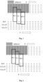
- Fig. 1 when the first red light-emitting device is in the starting state, the relationship between the activation energies of the hole transport layer, the compensation layer, and the light-emitting layer is shown in Fig. 1 , wherein HT-1 represents the hole transport layer, R'-1 represents the red compensation layer, and RH-1 represents the red host material.
- F represents the hole injection direction
- E represents the electron injection direction
- the activation energy of the hole transport layer is less than the activation energy of the compensation layer
- the activation energy of the compensation layer is less than the activation energy of the red host material.
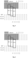
- the relationship between the activation energies of the hole transport layer, the compensation layer, and the light-emitting layer is shown in Fig. 2 .
- the activation energy of the hole transport layer is less than the activation energy of the compensation layer, and the activation energy of the compensation layer is less than the activation energy of the red host material.
- a second red light-emitting device including a hole transport layer, a compensation layer and a light-emitting layer is fabricated, and the starting voltage and the operating voltage thereof are tested.
- the light-emitting layer has a first red host material
- the second red light-emitting device of the experimental example 1 except that the compensation layer is different from the compensation layer in the comparative example 1, the rest of the functional layers are the same. That is, in the experimental example 1 and the comparative example 1, only the compensation layer is used as a variable.
- the relationship between the activation energies of the hole transport layer, the compensation layer, and the light-emitting layer is shown in Fig. 3 .
- the activation energy of the hole transport layer is less than the activation energy of the first red host material
- the activation energy of the compensation layer is higher than the activation energies of the first red host material and the hole transport layer.
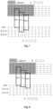
- the relationship between the activation energies of the hole transport layer, the compensation layer, and the light-emitting layer is shown in Fig. 4 .
- the activation energy of the hole transport layer is less than the activation energy of the compensation layer, and the activation energy of the compensation layer is less than the activation energy of the first red host material.
- Table 1 is the test experimental results of the comparative example 1 and the experimental example 1. starting state operating state Von@4 grayscale (V) Von@255 grayscale (V) Eff. (cd/A) comparative example 1 ⁇ Ea 1 >0 eV ⁇ Ea 4 >0 eV 2.07 3.33 54.8 experimental example 1 ⁇ Ea 1 ⁇ 0 eV ⁇ Ea 4 >0 eV 2.31 3.30 53.3
- the light-emitting device can resist the negative impact of the crosstalk current when the display panel is displayed at a low grayscale, and can avoid the problem of display color shift of the display panel. Further, the color rendering accuracy of the display panel (especially at low grayscale) is improved.
- the second group of experiments includes a comparative example 2 and an experimental example 2.
- a first green light-emitting device including a hole transport layer, a compensation layer and a light-emitting layer is fabricated, and the starting voltage and the operating voltage thereof are tested.
- the light-emitting layer in the hole-only device has a first green host material.
- the relationship between the activation energies of the hole transport layer, the compensation layer, and the light-emitting layer is shown in Fig. 5 .
- the activation energy of the hole transport layer is less than the activation energy of the compensation layer, and the activation energy of the compensation layer is less than the activation energy of the first green host material.
- the relationship between the activation energies of the hole transport layer, the compensation layer, and the light-emitting layer is shown in Fig. 6 .
- the activation energy of the hole transport layer is less than the activation energy of the compensation layer, and the activation energy of the compensation layer is less than the activation energy of the first green host material.
- a second green light-emitting device including a hole transport layer, a compensation layer and a light-emitting layer is fabricated, and the starting voltage and the operating voltage thereof are tested.
- the light-emitting layer has a first green host material
- the second green light-emitting device of the experimental example 2 except that the compensation layer is different from the compensation layer in the comparative example 2, the rest of the functional layers are the same. That is, in the experimental example 2 and the comparative example 2, only the compensation layer is used as a variable.
- the relationship between the activation energies of the hole transport layer, the compensation layer, and the light-emitting layer is shown in Fig. 7 .
- the activation energy of the hole transport layer is less than the activation energy of the first green host material
- the activation energy of the compensation layer is higher than the activation energies of the first green host material and the hole transport layer.
- the relationship between the activation energies of the hole transport layer, the compensation layer, and the light-emitting layer is shown in Fig. 8 .
- the activation energy of the hole transport layer is less than the activation energy of the compensation layer, and the activation energy of the compensation layer is less than the activation energy of the first green host material.
- Table 2 is the test experimental results of the comparative example 2 and the experimental example 2. starting state operating state Von@4 grayscale (V) Von@255 grayscale (V) Eff. (cd/A) comparative example 2 ⁇ Ea 1 >0 eV ⁇ Ea 4 >0 eV 2.18 3.58 160.1 experimental example 2 ⁇ Ea 1 ⁇ 0 eV ⁇ Ea 4 >0 eV 2.35 3.53 161.0
- the light-emitting device can resist the negative impact of the crosstalk current when the display panel is displayed at a low grayscale, and can avoid the problem of display color shift of the display panel. Further, the color rendering accuracy of the display panel (especially at low grayscale) is improved.
- an embodiment of the present application provides a display panel including the light-emitting device according to the above embodiment of the present application.
- the display panel provided by the embodiment of the present application has high color rendering accuracy and good display effect.
Landscapes
- Physics & Mathematics (AREA)
- Optics & Photonics (AREA)
- Engineering & Computer Science (AREA)
- Computer Hardware Design (AREA)
- General Physics & Mathematics (AREA)
- Theoretical Computer Science (AREA)
- Manufacturing & Machinery (AREA)
- Electroluminescent Light Sources (AREA)
- Devices For Indicating Variable Information By Combining Individual Elements (AREA)
Applications Claiming Priority (2)
| Application Number | Priority Date | Filing Date | Title |
|---|---|---|---|
| CN202011476315.5A CN114639786B (zh) | 2020-12-15 | 2020-12-15 | 发光器件及显示面板 |
| PCT/CN2021/118821 WO2022127231A1 (zh) | 2020-12-15 | 2021-09-16 | 发光器件及显示面板 |
Publications (2)
| Publication Number | Publication Date |
|---|---|
| EP4210120A1 true EP4210120A1 (de) | 2023-07-12 |
| EP4210120A4 EP4210120A4 (de) | 2024-07-03 |
Family
ID=81945010
Family Applications (1)
| Application Number | Title | Priority Date | Filing Date |
|---|---|---|---|
| EP21905163.8A Pending EP4210120A4 (de) | 2020-12-15 | 2021-09-16 | Lichtemittierende vorrichtung und anzeigetafel |
Country Status (6)
| Country | Link |
|---|---|
| US (1) | US11972733B2 (de) |
| EP (1) | EP4210120A4 (de) |
| JP (1) | JP7589342B2 (de) |
| KR (1) | KR20230051599A (de) |
| CN (1) | CN114639786B (de) |
| WO (1) | WO2022127231A1 (de) |
Family Cites Families (13)
| Publication number | Priority date | Publication date | Assignee | Title |
|---|---|---|---|---|
| US6881502B2 (en) | 2003-09-24 | 2005-04-19 | Eastman Kodak Company | Blue organic electroluminescent devices having a non-hole-blocking layer |
| DE10351822B4 (de) * | 2003-10-29 | 2008-10-02 | Samsung SDI Co., Ltd., Suwon | OLED-Bauelement und Display auf Basis von OLED-Bauelementen mit verbesserter Effizienz |
| US8101290B2 (en) | 2007-10-17 | 2012-01-24 | Technical Institute Of Physics And Chemistry Of Chinese Academy Of Sciences | Organic compound having electron-transporting and/or hole-blocking performance and its use and OLEDs comprising the compound |
| CN204289453U (zh) | 2014-12-24 | 2015-04-22 | 昆山国显光电有限公司 | 一种有机发光显示器件 |
| KR102857431B1 (ko) * | 2016-12-30 | 2025-09-09 | 엘지디스플레이 주식회사 | 백색 유기 발광 소자 및 이를 이용한 유기 발광 표시 장치 |
| CN108336237B (zh) * | 2017-01-20 | 2020-01-31 | 昆山工研院新型平板显示技术中心有限公司 | 一种有机电致发光器件 |
| CN116583131A (zh) * | 2017-04-26 | 2023-08-11 | Oti照明公司 | 用于图案化表面上覆层的方法和包括图案化覆层的装置 |
| CN108807481B (zh) * | 2018-06-13 | 2020-10-27 | 上海天马有机发光显示技术有限公司 | 一种有机发光显示面板及显示装置 |
| CN109346500B (zh) * | 2018-06-29 | 2020-12-01 | 云谷(固安)科技有限公司 | 一种有机电致发光装置 |
| CN108963093B (zh) * | 2018-06-29 | 2020-05-08 | 云谷(固安)科技有限公司 | 有机电致发光器件和有机电致发光装置 |
| CN208955023U (zh) | 2018-10-23 | 2019-06-07 | 宸鸿光电科技股份有限公司 | 有机发光二极管显示装置 |
| CN114843413B (zh) * | 2020-06-11 | 2025-12-02 | 云谷(固安)科技有限公司 | 发光器件及显示面板 |
| CN111697147B (zh) * | 2020-06-11 | 2022-09-06 | 云谷(固安)科技有限公司 | 发光器件及显示面板 |
-
2020
- 2020-12-15 CN CN202011476315.5A patent/CN114639786B/zh active Active
-
2021
- 2021-09-16 JP JP2023521623A patent/JP7589342B2/ja active Active
- 2021-09-16 KR KR1020237010928A patent/KR20230051599A/ko not_active Ceased
- 2021-09-16 EP EP21905163.8A patent/EP4210120A4/de active Pending
- 2021-09-16 WO PCT/CN2021/118821 patent/WO2022127231A1/zh not_active Ceased
-
2023
- 2023-02-14 US US18/168,820 patent/US11972733B2/en active Active
Also Published As
| Publication number | Publication date |
|---|---|
| JP7589342B2 (ja) | 2024-11-25 |
| JP2023544860A (ja) | 2023-10-25 |
| US11972733B2 (en) | 2024-04-30 |
| EP4210120A4 (de) | 2024-07-03 |
| CN114639786B (zh) | 2025-08-22 |
| WO2022127231A1 (zh) | 2022-06-23 |
| CN114639786A (zh) | 2022-06-17 |
| US20230186857A1 (en) | 2023-06-15 |
| KR20230051599A (ko) | 2023-04-18 |
Similar Documents
| Publication | Publication Date | Title |
|---|---|---|
| TWI819371B (zh) | 液晶顯示裝置 | |
| US10916614B2 (en) | Array substrate, display panel, light-detecting method therefor and method for controlling the same | |
| CN103325318B (zh) | 显示基板和显示装置 | |
| CN105280684A (zh) | 一种oled显示面板及其制备方法 | |
| CN104269429A (zh) | 一种有机电致发光显示器件、其驱动方法及显示装置 | |
| US12203972B2 (en) | Display panel and burn-in test method of the display panel | |
| Hack et al. | Performance of high‐efficiency AMOLED displays | |
| CN105845843A (zh) | 有机发光显示面板及其检测以及补偿方法 | |
| CN105097875A (zh) | 有机电致发光显示器件、显示装置及其制作方法 | |
| EP4210120A1 (de) | Lichtemittierende vorrichtung und anzeigetafel | |
| US11362313B2 (en) | Manufacturing method and processing device for display substrate each applying magnetic field during aging current being generated | |
| CN111613547B (zh) | 基板及膜层材料确定方法、制造方法、测试系统 | |
| CN114582942A (zh) | 发光器件的设计方法、发光器件及显示装置 | |
| EP4697910A1 (de) | Organische lichtemittierende anzeigetafel | |
| CN114639790B (zh) | 发光器件、材料筛选方法及显示面板 | |
| CN105428544A (zh) | 一种有机发光二极管结构 | |
| CN114628608A (zh) | 显示基板及显示装置 | |
| US8143780B2 (en) | Organic electroluminescent structure having a red color luminescent-electron transport layer | |
| CN113130797B (zh) | 有机电子元件、包括其的显示面板和包括其的显示装置 | |
| US20260090205A1 (en) | Display device including organic light emitting element and electronic device including the display device | |
| EP4207324A1 (de) | Lichtemittierende vorrichtung, materialscreeningverfahren und anzeigetafel | |
| CN114639779B (zh) | 材料筛选方法、发光器件及显示面板 | |
| CN114639787B (zh) | 发光器件及其制作方法、材料筛选方法、显示面板 | |
| Chen et al. | P‐163: The Optimization of Various Range Voltage in OLED According to Energy Level And Mobility Respectively | |
| CN203232657U (zh) | 显示基板和显示装置 |
Legal Events
| Date | Code | Title | Description |
|---|---|---|---|
| STAA | Information on the status of an ep patent application or granted ep patent |
Free format text: STATUS: THE INTERNATIONAL PUBLICATION HAS BEEN MADE |
|
| PUAI | Public reference made under article 153(3) epc to a published international application that has entered the european phase |
Free format text: ORIGINAL CODE: 0009012 |
|
| STAA | Information on the status of an ep patent application or granted ep patent |
Free format text: STATUS: REQUEST FOR EXAMINATION WAS MADE |
|
| 17P | Request for examination filed |
Effective date: 20230406 |
|
| AK | Designated contracting states |
Kind code of ref document: A1 Designated state(s): AL AT BE BG CH CY CZ DE DK EE ES FI FR GB GR HR HU IE IS IT LI LT LU LV MC MK MT NL NO PL PT RO RS SE SI SK SM TR |
|
| DAV | Request for validation of the european patent (deleted) | ||
| DAX | Request for extension of the european patent (deleted) | ||
| REG | Reference to a national code |
Ref country code: DE Ref legal event code: R079 Free format text: PREVIOUS MAIN CLASS: H01L0051500000 Ipc: H10K0050110000 |
|
| A4 | Supplementary search report drawn up and despatched |
Effective date: 20240531 |
|
| RIC1 | Information provided on ipc code assigned before grant |
Ipc: H10K 101/40 20230101ALN20240524BHEP Ipc: H10K 50/17 20230101ALN20240524BHEP Ipc: H10K 50/16 20230101ALI20240524BHEP Ipc: H10K 50/11 20230101AFI20240524BHEP |
|
| STAA | Information on the status of an ep patent application or granted ep patent |
Free format text: STATUS: EXAMINATION IS IN PROGRESS |
|
| 17Q | First examination report despatched |
Effective date: 20250620 |