EP4210184B1 - Dispositif laser modulé par électro-absorption pour l'intégration d'une puce retournée - Google Patents
Dispositif laser modulé par électro-absorption pour l'intégration d'une puce retournée Download PDFInfo
- Publication number
- EP4210184B1 EP4210184B1 EP22305015.4A EP22305015A EP4210184B1 EP 4210184 B1 EP4210184 B1 EP 4210184B1 EP 22305015 A EP22305015 A EP 22305015A EP 4210184 B1 EP4210184 B1 EP 4210184B1
- Authority
- EP
- European Patent Office
- Prior art keywords
- zone
- semi
- doped iii
- longitudinal axis
- layer
- Prior art date
- Legal status (The legal status is an assumption and is not a legal conclusion. Google has not performed a legal analysis and makes no representation as to the accuracy of the status listed.)
- Active
Links
Images



Classifications
-
- H—ELECTRICITY
- H01—ELECTRIC ELEMENTS
- H01S—DEVICES USING THE PROCESS OF LIGHT AMPLIFICATION BY STIMULATED EMISSION OF RADIATION [LASER] TO AMPLIFY OR GENERATE LIGHT; DEVICES USING STIMULATED EMISSION OF ELECTROMAGNETIC RADIATION IN WAVE RANGES OTHER THAN OPTICAL
- H01S5/00—Semiconductor lasers
- H01S5/02—Structural details or components not essential to laser action
- H01S5/026—Monolithically integrated components, e.g. waveguides, monitoring photo-detectors, drivers
- H01S5/0265—Intensity modulators
-
- H—ELECTRICITY
- H01—ELECTRIC ELEMENTS
- H01S—DEVICES USING THE PROCESS OF LIGHT AMPLIFICATION BY STIMULATED EMISSION OF RADIATION [LASER] TO AMPLIFY OR GENERATE LIGHT; DEVICES USING STIMULATED EMISSION OF ELECTROMAGNETIC RADIATION IN WAVE RANGES OTHER THAN OPTICAL
- H01S5/00—Semiconductor lasers
- H01S5/005—Optical components external to the laser cavity, specially adapted therefor, e.g. for homogenisation or merging of the beams or for manipulating laser pulses, e.g. pulse shaping
-
- H—ELECTRICITY
- H01—ELECTRIC ELEMENTS
- H01S—DEVICES USING THE PROCESS OF LIGHT AMPLIFICATION BY STIMULATED EMISSION OF RADIATION [LASER] TO AMPLIFY OR GENERATE LIGHT; DEVICES USING STIMULATED EMISSION OF ELECTROMAGNETIC RADIATION IN WAVE RANGES OTHER THAN OPTICAL
- H01S5/00—Semiconductor lasers
- H01S5/02—Structural details or components not essential to laser action
- H01S5/0206—Substrates, e.g. growth, shape, material, removal or bonding
- H01S5/0207—Substrates having a special shape
-
- H—ELECTRICITY
- H01—ELECTRIC ELEMENTS
- H01S—DEVICES USING THE PROCESS OF LIGHT AMPLIFICATION BY STIMULATED EMISSION OF RADIATION [LASER] TO AMPLIFY OR GENERATE LIGHT; DEVICES USING STIMULATED EMISSION OF ELECTROMAGNETIC RADIATION IN WAVE RANGES OTHER THAN OPTICAL
- H01S5/00—Semiconductor lasers
- H01S5/02—Structural details or components not essential to laser action
- H01S5/022—Mountings; Housings
- H01S5/0233—Mounting configuration of laser chips
- H01S5/0234—Up-side down mountings, e.g. Flip-chip, epi-side down mountings or junction down mountings
-
- H—ELECTRICITY
- H01—ELECTRIC ELEMENTS
- H01S—DEVICES USING THE PROCESS OF LIGHT AMPLIFICATION BY STIMULATED EMISSION OF RADIATION [LASER] TO AMPLIFY OR GENERATE LIGHT; DEVICES USING STIMULATED EMISSION OF ELECTROMAGNETIC RADIATION IN WAVE RANGES OTHER THAN OPTICAL
- H01S5/00—Semiconductor lasers
- H01S5/04—Processes or apparatus for excitation, e.g. pumping, e.g. by electron beams
- H01S5/042—Electrical excitation ; Circuits therefor
- H01S5/0425—Electrodes, e.g. characterised by the structure
- H01S5/04256—Electrodes, e.g. characterised by the structure characterised by the configuration
- H01S5/04257—Electrodes, e.g. characterised by the structure characterised by the configuration having positive and negative electrodes on the same side of the substrate
-
- H—ELECTRICITY
- H01—ELECTRIC ELEMENTS
- H01S—DEVICES USING THE PROCESS OF LIGHT AMPLIFICATION BY STIMULATED EMISSION OF RADIATION [LASER] TO AMPLIFY OR GENERATE LIGHT; DEVICES USING STIMULATED EMISSION OF ELECTROMAGNETIC RADIATION IN WAVE RANGES OTHER THAN OPTICAL
- H01S5/00—Semiconductor lasers
- H01S5/10—Construction or shape of the optical resonator, e.g. extended or external cavity, coupled cavities, bent-guide, varying width, thickness or composition of the active region
- H01S5/12—Construction or shape of the optical resonator, e.g. extended or external cavity, coupled cavities, bent-guide, varying width, thickness or composition of the active region the resonator having a periodic structure, e.g. in distributed feedback [DFB] lasers
-
- H—ELECTRICITY
- H01—ELECTRIC ELEMENTS
- H01S—DEVICES USING THE PROCESS OF LIGHT AMPLIFICATION BY STIMULATED EMISSION OF RADIATION [LASER] TO AMPLIFY OR GENERATE LIGHT; DEVICES USING STIMULATED EMISSION OF ELECTROMAGNETIC RADIATION IN WAVE RANGES OTHER THAN OPTICAL
- H01S5/00—Semiconductor lasers
- H01S5/20—Structure or shape of the semiconductor body to guide the optical wave ; Confining structures perpendicular to the optical axis, e.g. index or gain guiding, stripe geometry, broad area lasers, gain tailoring, transverse or lateral reflectors, special cladding structures, MQW barrier reflection layers
- H01S5/22—Structure or shape of the semiconductor body to guide the optical wave ; Confining structures perpendicular to the optical axis, e.g. index or gain guiding, stripe geometry, broad area lasers, gain tailoring, transverse or lateral reflectors, special cladding structures, MQW barrier reflection layers having a ridge or stripe structure
- H01S5/2205—Structure or shape of the semiconductor body to guide the optical wave ; Confining structures perpendicular to the optical axis, e.g. index or gain guiding, stripe geometry, broad area lasers, gain tailoring, transverse or lateral reflectors, special cladding structures, MQW barrier reflection layers having a ridge or stripe structure comprising special burying or current confinement layers
- H01S5/2222—Structure or shape of the semiconductor body to guide the optical wave ; Confining structures perpendicular to the optical axis, e.g. index or gain guiding, stripe geometry, broad area lasers, gain tailoring, transverse or lateral reflectors, special cladding structures, MQW barrier reflection layers having a ridge or stripe structure comprising special burying or current confinement layers having special electric properties
- H01S5/2224—Structure or shape of the semiconductor body to guide the optical wave ; Confining structures perpendicular to the optical axis, e.g. index or gain guiding, stripe geometry, broad area lasers, gain tailoring, transverse or lateral reflectors, special cladding structures, MQW barrier reflection layers having a ridge or stripe structure comprising special burying or current confinement layers having special electric properties semi-insulating semiconductors
-
- H—ELECTRICITY
- H01—ELECTRIC ELEMENTS
- H01S—DEVICES USING THE PROCESS OF LIGHT AMPLIFICATION BY STIMULATED EMISSION OF RADIATION [LASER] TO AMPLIFY OR GENERATE LIGHT; DEVICES USING STIMULATED EMISSION OF ELECTROMAGNETIC RADIATION IN WAVE RANGES OTHER THAN OPTICAL
- H01S5/00—Semiconductor lasers
- H01S5/20—Structure or shape of the semiconductor body to guide the optical wave ; Confining structures perpendicular to the optical axis, e.g. index or gain guiding, stripe geometry, broad area lasers, gain tailoring, transverse or lateral reflectors, special cladding structures, MQW barrier reflection layers
- H01S5/22—Structure or shape of the semiconductor body to guide the optical wave ; Confining structures perpendicular to the optical axis, e.g. index or gain guiding, stripe geometry, broad area lasers, gain tailoring, transverse or lateral reflectors, special cladding structures, MQW barrier reflection layers having a ridge or stripe structure
- H01S5/227—Buried mesa structure ; Striped active layer
- H01S5/2275—Buried mesa structure ; Striped active layer mesa created by etching
-
- H—ELECTRICITY
- H01—ELECTRIC ELEMENTS
- H01S—DEVICES USING THE PROCESS OF LIGHT AMPLIFICATION BY STIMULATED EMISSION OF RADIATION [LASER] TO AMPLIFY OR GENERATE LIGHT; DEVICES USING STIMULATED EMISSION OF ELECTROMAGNETIC RADIATION IN WAVE RANGES OTHER THAN OPTICAL
- H01S5/00—Semiconductor lasers
- H01S5/02—Structural details or components not essential to laser action
- H01S5/028—Coatings ; Treatment of the laser facets, e.g. etching, passivation layers or reflecting layers
- H01S5/0287—Facet reflectivity
-
- H—ELECTRICITY
- H01—ELECTRIC ELEMENTS
- H01S—DEVICES USING THE PROCESS OF LIGHT AMPLIFICATION BY STIMULATED EMISSION OF RADIATION [LASER] TO AMPLIFY OR GENERATE LIGHT; DEVICES USING STIMULATED EMISSION OF ELECTROMAGNETIC RADIATION IN WAVE RANGES OTHER THAN OPTICAL
- H01S5/00—Semiconductor lasers
- H01S5/10—Construction or shape of the optical resonator, e.g. extended or external cavity, coupled cavities, bent-guide, varying width, thickness or composition of the active region
- H01S5/12—Construction or shape of the optical resonator, e.g. extended or external cavity, coupled cavities, bent-guide, varying width, thickness or composition of the active region the resonator having a periodic structure, e.g. in distributed feedback [DFB] lasers
- H01S5/125—Distributed Bragg reflector [DBR] lasers
Definitions
- Various example embodiments relate to optoelectronic devices such as Electro-absorption Modulated Lasers (usually known by the acronym EML).
- EML Electro-absorption Modulated Lasers
- embodiments according to the invention relate to the realization of such optoelectronic devices which are based on an one-step process of a Semi-insulated Buried Heterostructure (usually known by the acronym SiBH).
- an EML is a laser diode integrated with an electro-absorption modulator (usually known by the acronym EAM) in a single chip. It can be applied to high frequency telecommunications (up to 100 Gbit/s) and long-distance transmission (10 km to 100 km) applications, because of its low chromatic dispersion.
- the laser diode section operates under a continuous wave condition (CW), and on/off voltage input signals are applied to the EAM section to generate optical output signals. The properties of the laser are not altered by the modulation process.
- the frequency response up to 100 GHz of an EML depends on a capacitance in the EAM section.
- the extinction in an EML is generated by the voltage modulated absorption of the EAM section.
- SiBH Semi-insulated Buried Heterostructure
- EML electro-absorbtion modulated laser
- SOA semiconductor optical amplifiers
- EP 3416252A1 teaches a simplified one-step method for making a SIBH structure allowing electrical isolation between electrodes without the need for ion implantation.
- EP 3416252A1 presents some drawbacks.
- the optoelectronic device with SiBH obtained by this technology is not flat, especially around the waveguide, because of the different growths of the [100] [110] or [111] crystalline plans.
- the metal contacts are not at the same level. It imposes to generate pillars for the via contact on the device or on the flip chip package.
- Example embodiments of the invention aim to remedy all or some of the disadvantages of the above identified prior art.
- EML electro-absorption modulated laser
- the electro-absorption modulated laser may further comprise a dielectric mirror R max positioned at the end of the first zone opposite to first electrical separation.
- the electro-absorption modulated laser may further comprise:
- Embodiments of the invention as claimed further provide a method of fabricating an electro-absorption modulated laser device (usually known by the acronym EML) comprising:
- the active material stack (such as Multi Quantum Wells based on AlGaInP or GaInAsP) can be of different natures in the first and second zones by performing Selective Area Growth epitaxy or Butt-joint Technology.
- the method of fabricating may further comprise between steps I and J, a step I' of chemical and/or mechanical surface stripping of the regrown semi-insulating stack, to flatten it to the level of the top of the side walls.
- the method may further comprise the following step to obtain an electro-absorption modulated laser device according to the first example of the general embodiment (or first embodiment): step K of forming the first electrical separation is followed by a step L of positioning a dielectric mirror R max at the end of the first zone opposite to first electrical separation.
- the method may further comprise the following steps to obtain an electro-absorption modulated laser device according to the second example of the general embodiment (or second embodiment):
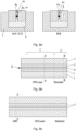
- FIG. 1 schematically represents two sectional views of Semi-Insulating Buried Heterostructures (SIBH) realized by a state-of-the-art one-step process of manufacture.
- SIBH Semi-Insulating Buried Heterostructures
- FIG. 1 shows that a p metal contact 8 is deposited on a p-doped III-V semiconductor 4 and/or on the front side of the n doped III-V semiconductor 2 (see FIG. 1 , right scheme).
- the last solution implies the etching of a via 70 in the SIBH layer 7 until reaching a doped III-V layer 2 connected to the III-V substrate 1.
- the optoelectronic device with SiBH obtained by this technology is not flat, especially around the waveguide 3, because of the different growths of the [100] [110] or [111] crystalline layers.
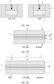
- FIG. 2 schematically represents the two sectional views of Semi-Insulating Buried Heterostructures (SIBH) of FIG. 1 in which pillars 71, 72 are generated for obtaining structures with metal contacts 8 at the same level, one of the structures being encapsulated in a resin R for overcoming mechanical weakness issues (see FIG. 2 , right scheme 2).
- SIBH Semi-Insulating Buried Heterostructures
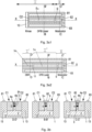
- FIGs. 3a to 3c schematically represent two specific embodiments of an EML device D according to the present invention that overcomes the above-mentioned drawbacks.
- FIG. 3a shows two respective top views ( FIG. 3a1 and FIG. 3a2 ) of these two respective embodiments of the EML device D.
- FIG. 3a1 shows a first embodiment of the EML device comprising a combination of DFB laser and R max mirror and
- FIG.3a2 shows a second embodiment of the EML device comprising a combination of DFB laser and a distributed Bragg Reflector DBR.
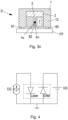
- FIG. 3b (middle and right parts) show two sectional views of the SiBH heterostructures of these embodiments according to the B-B' and C-C' planes applying to both examples, and another sectional view (left part of Fig. 3b ) according to plane D-D' applying only to the second embodiment of FIG.3a2 ;
- FIG. 3c shows an additional sectional view of both embodiments of the EML device according to the C-C' plane, with the EML device being flip-chipped on an electronic package.
- FIGs. 3a1, 3a2 and 3b show that it comprises:
- FIG. 3c shows that the metal contacts 81, 82, 83 are soldered on the flip-chip package FP.
- the EML device thus comprises a laser working in a continuous wave condition (corresponding to the optical waveguide 3 of the first zone I) and an EAM modulated in order to reach high frequencies without a limitation of optical power (corresponding to the optical waveguide 3 in the second zone, without DFB grating or DBR).
- the optical modulated signal is emitted by the front face of the device which is at the right of Figures 3a1 and 3a2 .
- the optical functions integration is based on a single MQW layer (acronym for Multi Quantum Wells).
- the DFB grating 5a allows to define the laser wavelength.
- figure 3a1 shows that EML device D may further comprise a dielectric mirror R max 10 positioned at the end of the first zone I opposite to first electrical separation 9, that is to say on the rear face of the laser.
- EML device D comprises:
- FIG. 4 schematically represents the electrical scheme or equivalent circuit of the EML device: the laser function in zone I is powered by a current generator CG and the EAM function in zone II is reverse polarized by a voltage generator VG. Both current generator CG and voltage generator VG are not shown on figures 3a-c as they are lying outside of the EML laser and are connectable to the device D using the contact layers 81,82,83 .They can be made using state-of-the art techniques and be connected to the device D via cables, wires or electronic paths.
- FIGs. 5 to 10 schematically represent the different steps of the process flow for fabricating an EML device D according to the embodiments represented in figure 3 .
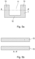
- FIG. 5a schematically represents step A of providing a substrate 1 made of III-V semiconductor material
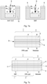
- FIGs. 6a to 6c shows that the substrate 1 is then etched to form a groove 11 along a longitudinal axis of U-shaped cross-section and thus defining a base 12 and side walls 13 (step B) .
- a stack of layers comprising a layer of n-doped III-V semiconductor 2 on the base 1), an active material stack 3' on said layer of n-doped III-V semi-conductor 2, first p-doped III-V semiconductor 4a (such as InP),second p-doped III-V semi-conductors (such as InP and AlGaInP or GaInAsP) constituting the grating layers 5 are epitaxied (step C .
- first p-doped III-V semiconductor 4a such as InP
- second p-doped III-V semi-conductors such as InP and AlGaInP or GaInAsP
- a Distributed Feedback Grating 5a is etched in the grating layers 5 (step D), the remaining zone constituting the second zone II (for both examples: see FIGs. 6a to 6c ).
- step D may further comprise the etching of a DBR 5b inside the grating layers 5 within a first sub-zone I' located along the axis XX in the first zone I and outside the part of the first zone I containing the Distributed Feedback Grating 5a which constitutes the second sub-zone I" (for the second example only).
- step E the Distributed Bragg Reflector 5b and the Distributed Feedback Grating 5a are buried simultaneously by the layer 4 of p-doped III-V semi-conductor.
- FIG. 7 shows that step E is followed by a step G of depositing a dielectric mask 6 on the layer of p-doped III-V semi-conductor 4. This step is followed by a step H of etching, along the axis XX, two channels C1, C2 at least below the level of the active material stack 3', each channel C1, C2 being located along each side wall 13 of the substrate 1, so as to define a central stripe portion S comprising the etched material stack 3 constituting the optical waveguide 3 and the etched layer of p-doped III-V semiconductor 4.
- FIGs. 8a to 8c show that a semi-insulating stack 7 is regrown at least up to the level of the top of the layer of the p-doped III-V semi-conductor contact layer 4b (step I).
- FIG. 9 shows that step I of regrowth is followed by the removing the remaining dielectric mask 6 (step J). If stack 7 is regrown over the n InP substrate, there may be an optional step J' of chemical and/or mechanical surface stripping of the stack 7, to flatten it to the level of the top of the side walls 13.
- FIG. 3a1 to c shows, for both examples of the EML device D, that metal stripes 81, 82, 83 are formed (step K) along the axis XX (see notably FIG. 3a ) and on the top of the side walls 13 and on the top of the central stripe portion (see notably FIGs. 3a1, 3a2 and 3b ).
- Step K is followed (for both embodiments: see FIGs. 3b and 3c ) by step L of forming a first electrical separation 9 between the first I and second zones II by implanting H+ ions within a thin ribbon of implanted H+ located between the side walls 13 and perpendicular to the axis XX.
- the step L of forming the first electrical separation 9 may be followed by a step M of positioning a dielectric mirror R max 10 at the end of the first zone I opposite to the first electrical separation 9, so as to obtain an EML device D according to the first example of the general embodiment.
- step L further comprises the forming of a second electrical separation 11 between the first I' and the second sub-zone I" by implanting H+ ions within another thin ribbon of implanted H+ located between the side walls 13 and perpendicular to the axis XX, provided that a DBR 5' has been previously etched into the p-doped III-V semiconductor layer 4 in step F (see above).
Landscapes
- Physics & Mathematics (AREA)
- Condensed Matter Physics & Semiconductors (AREA)
- General Physics & Mathematics (AREA)
- Electromagnetism (AREA)
- Optics & Photonics (AREA)
- Geometry (AREA)
- Semiconductor Lasers (AREA)
Claims (7)
- Dispositif laser modulé par électro-absorption (D) comprenant :- un substrat (1) réalisé en un matériau semi-conducteur III-V présentant une base (12) et des parois latérales (13) et ayant un axe longitudinal (XX), ledit substrat (1) étant gravé pour former une rainure (11) de section transversale en forme de U,- une couche d'un semi-conducteur III-V dopé n (2) disposée sur la base (12) à l'intérieur de ladite rainure (11) ;- une portion de bande (S) centrale comprenant un guide d'ondes (3) enterré sur lequel on fait croître une couche de semi-conducteur III-V dopé p (4a) et une couche de contact de semi-conducteur III-V dopé p (4b) au moins jusqu'en haut des parois latérales (13) ;- deux canaux (C1, C2) gravés dans la couche de semi-conducteur III-V dopé n (2) le long de l'axe longitudinal (XX) et situés le long de chaque paroi latérale (13) des deux côtés de la portion de bande (S) centrale, lesdits canaux (C1, C2) étant chacun remplis d'un empilement semi-isolant (7) mis à nouveau à croître jusqu'en haut de la couche de contact de semi-conducteur III-V dopé p (4b) ;- dans une zone de la portion de bande (S) centrale à côté de l'axe longitudinal (XX) constituant la première zone (I), un réseau à rétroaction distribuée (5a) gravé à l'intérieur de la couche de semi-conducteur III-V dopé p (4), la zone restante constituant la deuxième zone (II) ;- des bandes métalliques (81, 82, 83) disposées sur le haut des parois latérales (13) et sur le haut de ladite portion de bande (S) ;- une première séparation électrique (9) entre la première zone (I) et la deuxième zone (II) consistant en un mince ruban de H+ implanté situé entre les parois latérales (13) et perpendiculaire à l'axe longitudinal (XX).
- Dispositif laser modulé par électro-absorption (D) selon la revendication 1, comprenant en outre un miroir diélectrique Rmax (10) positionné à l'extrémité de la première zone (I) opposée à une première séparation électrique (9).
- Dispositif laser modulé par électro-absorption (D) selon l'une des revendications 1 et 2, comprenant en outre :- un réflecteur de Bragg distribué (DBR) (5b) gravé à l'intérieur de la couche de semi-conducteur III-V dopé p (4) dans une première sous-zone (I') située le long dudit axe longitudinal (XX) de la première zone (I) et à l'extérieur de la partie de la première zone (I) contenant le réseau à rétroaction distribuée (5a) qui constitue la deuxième sous-zone (I") ; et- une deuxième séparation électrique (11) entre la première sous-zone (I') et la deuxième sous-zone (I") consistant en un autre mince ruban de H+ implanté situé entre les parois latérales (13) et perpendiculaire à l'axe longitudinal (XX).
- Procédé de fabrication d'un dispositif laser modulé par électro-absorption (D) selon l'une des revendications 1 à 3, ledit procédé comprenant les étapes suivantes :A. fournir un substrat (1) réalisé en un matériau semi-conducteur III-V ayant un axe longitudinal (XX),B. graver ledit substrat (1) pour former une rainure (11) de section transversale en forme de U et pour définir ainsi une base (12) et des parois latérales (13) ;C. réaliser une croissance épitaxiale d'un empilement de couches comprenant une couche d'un semi-conducteur III-V dopé n (2) sur la base (12), un empilement de matériau actif (3') sur ladite couche d'un semi-conducteur III-V dopé n (2), et des semi-conducteurs III-V dopés p (tels que InP et AlGaInP ou GaInAsP) constituant les couches de réseau (5) ;D. dans une zone d'un dispositif laser modulé par électro-absorption (D) à côté dudit axe longitudinal (XX) constituant la première zone (I), graver un réseau à rétroaction distribuée (5a) à l'intérieur des couches de réseau (5), la zone restante constituant la deuxième zone (II) ;E. réaliser une croissance épitaxiale d'une couche (4a) d'un semi-conducteur III-V dopé p (4a) et d'une couche de contact de semi-conducteur III-V dopé p (4b) pour enterrer ledit réseau à rétroaction distribuée (5a) ;F. déposer un masque diélectrique (6) sur la couche de semi-conducteur III-V dopé p (4) ;G. graver, le long de l'axe longitudinal (XX), deux canaux (C1, C2) au moins au-dessous du niveau de l'empilement de matériau actif (3'), chaque canal (C1, C2) étant situé le long de chaque paroi latérale (13) du substrat (1), de manière à définir une portion de bande (S) centrale comprenant l'empilement de matériau (3') gravé constituant le guide d'ondes (3) optique et la couche de semi-conducteur III-V dopé p (4) gravée ;H. réaliser une nouvelle croissance épitaxiale d'un empilement semi-isolant (7) jusqu'en haut de la couche de contact de semi-conducteur III-V dopé p (4b) ;I. retirer le masque diélectrique (7) restant ;J. déposer, le long dudit axe longitudinal (XX), trois bandes métalliques (81, 82, 83) sur le haut des parois latérales (13) et sur le haut de ladite portion de bande (S) centrale ;K. former une première séparation électrique (9) entre la première zone (I) et la deuxième zone (II) en implantant des ions H+ dans un mince ruban de H+ implanté situé entre les parois latérales (13) et perpendiculaire à l'axe longitudinal (XX).
- Procédé de fabrication selon la revendication 4, comprenant en outre, après l'étape K de formation de la première séparation électrique (9), une étape L de positionnement d'un miroir diélectrique Rmax (10) à l'extrémité de la première zone (I) opposée à la première séparation électrique (9).
- Procédé de fabrication selon la revendication 4,- dans lequel l'étape D comprend en outre la gravure d'un réflecteur de Bragg distribué (5b) à l'intérieur des couches de réseau (5) dans une première sous-zone (I') située le long dudit axe longitudinal (XX) de la première zone (I) et à l'extérieur de la partie de la première zone (I) contenant le réseau à rétroaction distribuée (5a) qui constitue la deuxième sous-zone (I"), la gravure du réflecteur de Bragg distribué (5b) et la gravure du réseau à rétroaction distribuée (5a) étant réalisées simultanément ;- dans lequel au cours de l'étape E), ledit réflecteur de Bragg distribué (5b) et ledit réseau à rétroaction distribuée (5a) sont enterrés simultanément par la couche (4) d'un semi-conducteur III-V dopé p ;- dans lequel l'étape K est suivie d'une étape M de formation d'une deuxième séparation électrique (11) entre la première sous-zone (I') et la deuxième sous-zone (I") en implantant des ions H+ dans un autre mince ruban de H+ implanté situé entre les parois latérales (13) et perpendiculaire à l'axe longitudinal (XX).
- Procédé de fabrication selon l'une des revendications 5 et 6, comprenant en outre, entre les étapes I et J, une étape I' de décapage chimique et/ou mécanique de la surface de l'empilement semi-isolant (7) mis à nouveau à croître, pour l'aplanir au niveau du haut des parois latérales (13).
Priority Applications (1)
| Application Number | Priority Date | Filing Date | Title |
|---|---|---|---|
| EP22305015.4A EP4210184B1 (fr) | 2022-01-10 | 2022-01-10 | Dispositif laser modulé par électro-absorption pour l'intégration d'une puce retournée |
Applications Claiming Priority (1)
| Application Number | Priority Date | Filing Date | Title |
|---|---|---|---|
| EP22305015.4A EP4210184B1 (fr) | 2022-01-10 | 2022-01-10 | Dispositif laser modulé par électro-absorption pour l'intégration d'une puce retournée |
Publications (2)
| Publication Number | Publication Date |
|---|---|
| EP4210184A1 EP4210184A1 (fr) | 2023-07-12 |
| EP4210184B1 true EP4210184B1 (fr) | 2024-07-24 |
Family
ID=79830952
Family Applications (1)
| Application Number | Title | Priority Date | Filing Date |
|---|---|---|---|
| EP22305015.4A Active EP4210184B1 (fr) | 2022-01-10 | 2022-01-10 | Dispositif laser modulé par électro-absorption pour l'intégration d'une puce retournée |
Country Status (1)
| Country | Link |
|---|---|
| EP (1) | EP4210184B1 (fr) |
Families Citing this family (1)
| Publication number | Priority date | Publication date | Assignee | Title |
|---|---|---|---|---|
| WO2021186695A1 (fr) * | 2020-03-19 | 2021-09-23 | 三菱電機株式会社 | Élément à semi-conducteur optique |
Family Cites Families (5)
| Publication number | Priority date | Publication date | Assignee | Title |
|---|---|---|---|---|
| JPH10256669A (ja) * | 1997-03-14 | 1998-09-25 | Mitsubishi Electric Corp | 光変調器集積半導体レーザダイオード |
| JP2004281686A (ja) * | 2003-03-14 | 2004-10-07 | Sumitomo Electric Ind Ltd | 半導体発光デバイス及びその製造方法 |
| CN107430293B (zh) * | 2015-03-23 | 2021-02-26 | 日本电信电话株式会社 | 光电路 |
| EP3416252A1 (fr) | 2017-06-13 | 2018-12-19 | Nokia Solutions and Networks Oy | Sibh en une étape pour circuits intégrés |
| GB2586889B (en) * | 2019-08-26 | 2022-11-02 | Rockley Photonics Ltd | Method of manufacturing a III-V based optoelectronic device |
-
2022
- 2022-01-10 EP EP22305015.4A patent/EP4210184B1/fr active Active
Also Published As
| Publication number | Publication date |
|---|---|
| EP4210184A1 (fr) | 2023-07-12 |
Similar Documents
| Publication | Publication Date | Title |
|---|---|---|
| US7112827B2 (en) | Tunable wavelength laser | |
| US6238943B1 (en) | Optical semiconductor device and a method of manufacturing the same | |
| KR102171268B1 (ko) | 하이브리드 실리콘 레이저 제조 방법 | |
| US6798807B2 (en) | Semiconductor laser and semiconductor laser module | |
| US20200335940A1 (en) | High-order bragg grating single-mode laser array | |
| US8488918B2 (en) | Semiconductor optical device, optical transmitter module, optical transceiver module, and optical transmission equipment | |
| JP2001142037A (ja) | 電界効果型光変調器および半導体光素子の製造方法 | |
| US5636237A (en) | Semiconductor laser device which makes it possible to realize high-speed modulation | |
| JP2943510B2 (ja) | 可変波長半導体レーザ装置 | |
| US20070223543A1 (en) | Laterally Implanted Electroabsorption Modulated Laser | |
| US11769988B2 (en) | Vertical-cavity surface-emitting laser (VCSEL) tuned through application of mechanical stress via a piezoelectric material | |
| CN112670823B (zh) | 电吸收调制激光器的制作方法 | |
| EP4210184B1 (fr) | Dispositif laser modulé par électro-absorption pour l'intégration d'une puce retournée | |
| US6931041B2 (en) | Integrated semiconductor laser device and method of manufacture thereof | |
| EP4210185A1 (fr) | Dispositif opto-électronique intégré pour l'intégration de billes | |
| US5346854A (en) | Method of making a semiconductor laser | |
| US20030137023A1 (en) | Optoelectronic device, and method for producing an optoelectronic device | |
| US7573925B1 (en) | Semiconductor laser having a doped active layer | |
| WO2009025912A2 (fr) | Optimisation des paramètres laser pour arriver à une performance souhaitée | |
| Bornholdt et al. | Passive optical GaInAsP/InP waveguides | |
| US7016558B2 (en) | Integrated optical device and fabricating method thereof | |
| EP1372229B1 (fr) | Element integré composé d'un laser semiconducteur et d'un guide d'ondes | |
| CN114678767A (zh) | 半导体光元件及其制造方法 | |
| KR100584332B1 (ko) | 전계흡수형 변조기가 집적된 레이저 장치 및 그 제조방법 | |
| JP3387751B2 (ja) | 偏波変調可能な半導体レーザ及びその製造方法 |
Legal Events
| Date | Code | Title | Description |
|---|---|---|---|
| PUAI | Public reference made under article 153(3) epc to a published international application that has entered the european phase |
Free format text: ORIGINAL CODE: 0009012 |
|
| STAA | Information on the status of an ep patent application or granted ep patent |
Free format text: STATUS: THE APPLICATION HAS BEEN PUBLISHED |
|
| AK | Designated contracting states |
Kind code of ref document: A1 Designated state(s): AL AT BE BG CH CY CZ DE DK EE ES FI FR GB GR HR HU IE IS IT LI LT LU LV MC MK MT NL NO PL PT RO RS SE SI SK SM TR |
|
| STAA | Information on the status of an ep patent application or granted ep patent |
Free format text: STATUS: REQUEST FOR EXAMINATION WAS MADE |
|
| 17P | Request for examination filed |
Effective date: 20230828 |
|
| RBV | Designated contracting states (corrected) |
Designated state(s): AL AT BE BG CH CY CZ DE DK EE ES FI FR GB GR HR HU IE IS IT LI LT LU LV MC MK MT NL NO PL PT RO RS SE SI SK SM TR |
|
| GRAP | Despatch of communication of intention to grant a patent |
Free format text: ORIGINAL CODE: EPIDOSNIGR1 |
|
| STAA | Information on the status of an ep patent application or granted ep patent |
Free format text: STATUS: GRANT OF PATENT IS INTENDED |
|
| INTG | Intention to grant announced |
Effective date: 20240227 |
|
| RIN1 | Information on inventor provided before grant (corrected) |
Inventor name: GARREAU, ALEXANDRE Inventor name: PARET, JEAN FRANCOIS |
|
| GRAJ | Information related to disapproval of communication of intention to grant by the applicant or resumption of examination proceedings by the epo deleted |
Free format text: ORIGINAL CODE: EPIDOSDIGR1 |
|
| STAA | Information on the status of an ep patent application or granted ep patent |
Free format text: STATUS: REQUEST FOR EXAMINATION WAS MADE |
|
| GRAS | Grant fee paid |
Free format text: ORIGINAL CODE: EPIDOSNIGR3 |
|
| STAA | Information on the status of an ep patent application or granted ep patent |
Free format text: STATUS: GRANT OF PATENT IS INTENDED |
|
| GRAP | Despatch of communication of intention to grant a patent |
Free format text: ORIGINAL CODE: EPIDOSNIGR1 |
|
| INTC | Intention to grant announced (deleted) | ||
| INTG | Intention to grant announced |
Effective date: 20240503 |
|
| GRAA | (expected) grant |
Free format text: ORIGINAL CODE: 0009210 |
|
| STAA | Information on the status of an ep patent application or granted ep patent |
Free format text: STATUS: THE PATENT HAS BEEN GRANTED |
|
| AK | Designated contracting states |
Kind code of ref document: B1 Designated state(s): AL AT BE BG CH CY CZ DE DK EE ES FI FR GB GR HR HU IE IS IT LI LT LU LV MC MK MT NL NO PL PT RO RS SE SI SK SM TR |
|
| REG | Reference to a national code |
Ref country code: GB Ref legal event code: FG4D |
|
| REG | Reference to a national code |
Ref country code: CH Ref legal event code: EP |
|
| REG | Reference to a national code |
Ref country code: IE Ref legal event code: FG4D Ref country code: DE Ref legal event code: R096 Ref document number: 602022004836 Country of ref document: DE |
|
| REG | Reference to a national code |
Ref country code: LT Ref legal event code: MG9D |
|
| REG | Reference to a national code |
Ref country code: NL Ref legal event code: MP Effective date: 20240724 |
|
| PG25 | Lapsed in a contracting state [announced via postgrant information from national office to epo] |
Ref country code: PT Free format text: LAPSE BECAUSE OF FAILURE TO SUBMIT A TRANSLATION OF THE DESCRIPTION OR TO PAY THE FEE WITHIN THE PRESCRIBED TIME-LIMIT Effective date: 20241125 |
|
| REG | Reference to a national code |
Ref country code: AT Ref legal event code: MK05 Ref document number: 1707200 Country of ref document: AT Kind code of ref document: T Effective date: 20240724 |
|
| PG25 | Lapsed in a contracting state [announced via postgrant information from national office to epo] |
Ref country code: NL Free format text: LAPSE BECAUSE OF FAILURE TO SUBMIT A TRANSLATION OF THE DESCRIPTION OR TO PAY THE FEE WITHIN THE PRESCRIBED TIME-LIMIT Effective date: 20240724 |
|
| PG25 | Lapsed in a contracting state [announced via postgrant information from national office to epo] |
Ref country code: PT Free format text: LAPSE BECAUSE OF FAILURE TO SUBMIT A TRANSLATION OF THE DESCRIPTION OR TO PAY THE FEE WITHIN THE PRESCRIBED TIME-LIMIT Effective date: 20241125 Ref country code: NL Free format text: LAPSE BECAUSE OF FAILURE TO SUBMIT A TRANSLATION OF THE DESCRIPTION OR TO PAY THE FEE WITHIN THE PRESCRIBED TIME-LIMIT Effective date: 20240724 |
|
| PG25 | Lapsed in a contracting state [announced via postgrant information from national office to epo] |
Ref country code: NO Free format text: LAPSE BECAUSE OF FAILURE TO SUBMIT A TRANSLATION OF THE DESCRIPTION OR TO PAY THE FEE WITHIN THE PRESCRIBED TIME-LIMIT Effective date: 20241024 |
|
| PG25 | Lapsed in a contracting state [announced via postgrant information from national office to epo] |
Ref country code: FI Free format text: LAPSE BECAUSE OF FAILURE TO SUBMIT A TRANSLATION OF THE DESCRIPTION OR TO PAY THE FEE WITHIN THE PRESCRIBED TIME-LIMIT Effective date: 20240724 Ref country code: PL Free format text: LAPSE BECAUSE OF FAILURE TO SUBMIT A TRANSLATION OF THE DESCRIPTION OR TO PAY THE FEE WITHIN THE PRESCRIBED TIME-LIMIT Effective date: 20240724 Ref country code: GR Free format text: LAPSE BECAUSE OF FAILURE TO SUBMIT A TRANSLATION OF THE DESCRIPTION OR TO PAY THE FEE WITHIN THE PRESCRIBED TIME-LIMIT Effective date: 20241025 |
|
| PG25 | Lapsed in a contracting state [announced via postgrant information from national office to epo] |
Ref country code: BG Free format text: LAPSE BECAUSE OF FAILURE TO SUBMIT A TRANSLATION OF THE DESCRIPTION OR TO PAY THE FEE WITHIN THE PRESCRIBED TIME-LIMIT Effective date: 20240724 |
|
| PG25 | Lapsed in a contracting state [announced via postgrant information from national office to epo] |
Ref country code: LV Free format text: LAPSE BECAUSE OF FAILURE TO SUBMIT A TRANSLATION OF THE DESCRIPTION OR TO PAY THE FEE WITHIN THE PRESCRIBED TIME-LIMIT Effective date: 20240724 |
|
| PG25 | Lapsed in a contracting state [announced via postgrant information from national office to epo] |
Ref country code: AT Free format text: LAPSE BECAUSE OF FAILURE TO SUBMIT A TRANSLATION OF THE DESCRIPTION OR TO PAY THE FEE WITHIN THE PRESCRIBED TIME-LIMIT Effective date: 20240724 Ref country code: IS Free format text: LAPSE BECAUSE OF FAILURE TO SUBMIT A TRANSLATION OF THE DESCRIPTION OR TO PAY THE FEE WITHIN THE PRESCRIBED TIME-LIMIT Effective date: 20241124 |
|
| PG25 | Lapsed in a contracting state [announced via postgrant information from national office to epo] |
Ref country code: HR Free format text: LAPSE BECAUSE OF FAILURE TO SUBMIT A TRANSLATION OF THE DESCRIPTION OR TO PAY THE FEE WITHIN THE PRESCRIBED TIME-LIMIT Effective date: 20240724 |
|
| PG25 | Lapsed in a contracting state [announced via postgrant information from national office to epo] |
Ref country code: ES Free format text: LAPSE BECAUSE OF FAILURE TO SUBMIT A TRANSLATION OF THE DESCRIPTION OR TO PAY THE FEE WITHIN THE PRESCRIBED TIME-LIMIT Effective date: 20240724 Ref country code: RS Free format text: LAPSE BECAUSE OF FAILURE TO SUBMIT A TRANSLATION OF THE DESCRIPTION OR TO PAY THE FEE WITHIN THE PRESCRIBED TIME-LIMIT Effective date: 20241024 |
|
| PG25 | Lapsed in a contracting state [announced via postgrant information from national office to epo] |
Ref country code: RS Free format text: LAPSE BECAUSE OF FAILURE TO SUBMIT A TRANSLATION OF THE DESCRIPTION OR TO PAY THE FEE WITHIN THE PRESCRIBED TIME-LIMIT Effective date: 20241024 Ref country code: PL Free format text: LAPSE BECAUSE OF FAILURE TO SUBMIT A TRANSLATION OF THE DESCRIPTION OR TO PAY THE FEE WITHIN THE PRESCRIBED TIME-LIMIT Effective date: 20240724 Ref country code: NO Free format text: LAPSE BECAUSE OF FAILURE TO SUBMIT A TRANSLATION OF THE DESCRIPTION OR TO PAY THE FEE WITHIN THE PRESCRIBED TIME-LIMIT Effective date: 20241024 Ref country code: LV Free format text: LAPSE BECAUSE OF FAILURE TO SUBMIT A TRANSLATION OF THE DESCRIPTION OR TO PAY THE FEE WITHIN THE PRESCRIBED TIME-LIMIT Effective date: 20240724 Ref country code: IS Free format text: LAPSE BECAUSE OF FAILURE TO SUBMIT A TRANSLATION OF THE DESCRIPTION OR TO PAY THE FEE WITHIN THE PRESCRIBED TIME-LIMIT Effective date: 20241124 Ref country code: HR Free format text: LAPSE BECAUSE OF FAILURE TO SUBMIT A TRANSLATION OF THE DESCRIPTION OR TO PAY THE FEE WITHIN THE PRESCRIBED TIME-LIMIT Effective date: 20240724 Ref country code: GR Free format text: LAPSE BECAUSE OF FAILURE TO SUBMIT A TRANSLATION OF THE DESCRIPTION OR TO PAY THE FEE WITHIN THE PRESCRIBED TIME-LIMIT Effective date: 20241025 Ref country code: FI Free format text: LAPSE BECAUSE OF FAILURE TO SUBMIT A TRANSLATION OF THE DESCRIPTION OR TO PAY THE FEE WITHIN THE PRESCRIBED TIME-LIMIT Effective date: 20240724 Ref country code: ES Free format text: LAPSE BECAUSE OF FAILURE TO SUBMIT A TRANSLATION OF THE DESCRIPTION OR TO PAY THE FEE WITHIN THE PRESCRIBED TIME-LIMIT Effective date: 20240724 Ref country code: BG Free format text: LAPSE BECAUSE OF FAILURE TO SUBMIT A TRANSLATION OF THE DESCRIPTION OR TO PAY THE FEE WITHIN THE PRESCRIBED TIME-LIMIT Effective date: 20240724 Ref country code: AT Free format text: LAPSE BECAUSE OF FAILURE TO SUBMIT A TRANSLATION OF THE DESCRIPTION OR TO PAY THE FEE WITHIN THE PRESCRIBED TIME-LIMIT Effective date: 20240724 |
|
| PG25 | Lapsed in a contracting state [announced via postgrant information from national office to epo] |
Ref country code: SM Free format text: LAPSE BECAUSE OF FAILURE TO SUBMIT A TRANSLATION OF THE DESCRIPTION OR TO PAY THE FEE WITHIN THE PRESCRIBED TIME-LIMIT Effective date: 20240724 Ref country code: DK Free format text: LAPSE BECAUSE OF FAILURE TO SUBMIT A TRANSLATION OF THE DESCRIPTION OR TO PAY THE FEE WITHIN THE PRESCRIBED TIME-LIMIT Effective date: 20240724 Ref country code: RO Free format text: LAPSE BECAUSE OF FAILURE TO SUBMIT A TRANSLATION OF THE DESCRIPTION OR TO PAY THE FEE WITHIN THE PRESCRIBED TIME-LIMIT Effective date: 20240724 |
|
| PG25 | Lapsed in a contracting state [announced via postgrant information from national office to epo] |
Ref country code: EE Free format text: LAPSE BECAUSE OF FAILURE TO SUBMIT A TRANSLATION OF THE DESCRIPTION OR TO PAY THE FEE WITHIN THE PRESCRIBED TIME-LIMIT Effective date: 20240724 |
|
| PG25 | Lapsed in a contracting state [announced via postgrant information from national office to epo] |
Ref country code: CZ Free format text: LAPSE BECAUSE OF FAILURE TO SUBMIT A TRANSLATION OF THE DESCRIPTION OR TO PAY THE FEE WITHIN THE PRESCRIBED TIME-LIMIT Effective date: 20240724 |
|
| REG | Reference to a national code |
Ref country code: DE Ref legal event code: R097 Ref document number: 602022004836 Country of ref document: DE |
|
| PG25 | Lapsed in a contracting state [announced via postgrant information from national office to epo] |
Ref country code: IT Free format text: LAPSE BECAUSE OF FAILURE TO SUBMIT A TRANSLATION OF THE DESCRIPTION OR TO PAY THE FEE WITHIN THE PRESCRIBED TIME-LIMIT Effective date: 20240724 Ref country code: SK Free format text: LAPSE BECAUSE OF FAILURE TO SUBMIT A TRANSLATION OF THE DESCRIPTION OR TO PAY THE FEE WITHIN THE PRESCRIBED TIME-LIMIT Effective date: 20240724 |
|
| PLBE | No opposition filed within time limit |
Free format text: ORIGINAL CODE: 0009261 |
|
| STAA | Information on the status of an ep patent application or granted ep patent |
Free format text: STATUS: NO OPPOSITION FILED WITHIN TIME LIMIT |
|
| 26N | No opposition filed |
Effective date: 20250425 |
|
| REG | Reference to a national code |
Ref country code: CH Ref legal event code: PL |
|
| PG25 | Lapsed in a contracting state [announced via postgrant information from national office to epo] |
Ref country code: SE Free format text: LAPSE BECAUSE OF FAILURE TO SUBMIT A TRANSLATION OF THE DESCRIPTION OR TO PAY THE FEE WITHIN THE PRESCRIBED TIME-LIMIT Effective date: 20240724 |
|
| PG25 | Lapsed in a contracting state [announced via postgrant information from national office to epo] |
Ref country code: LU Free format text: LAPSE BECAUSE OF NON-PAYMENT OF DUE FEES Effective date: 20250110 Ref country code: MC Free format text: LAPSE BECAUSE OF FAILURE TO SUBMIT A TRANSLATION OF THE DESCRIPTION OR TO PAY THE FEE WITHIN THE PRESCRIBED TIME-LIMIT Effective date: 20240724 |
|
| PG25 | Lapsed in a contracting state [announced via postgrant information from national office to epo] |
Ref country code: BE Free format text: LAPSE BECAUSE OF NON-PAYMENT OF DUE FEES Effective date: 20250131 |
|
| PG25 | Lapsed in a contracting state [announced via postgrant information from national office to epo] |
Ref country code: CH Free format text: LAPSE BECAUSE OF NON-PAYMENT OF DUE FEES Effective date: 20250131 |
|
| REG | Reference to a national code |
Ref country code: BE Ref legal event code: MM Effective date: 20250131 |
|
| PGFP | Annual fee paid to national office [announced via postgrant information from national office to epo] |
Ref country code: FR Payment date: 20251208 Year of fee payment: 5 |
|
| PG25 | Lapsed in a contracting state [announced via postgrant information from national office to epo] |
Ref country code: IE Free format text: LAPSE BECAUSE OF NON-PAYMENT OF DUE FEES Effective date: 20250110 |
|
| PGFP | Annual fee paid to national office [announced via postgrant information from national office to epo] |
Ref country code: DE Payment date: 20251203 Year of fee payment: 5 |