EP4210209A1 - Détection de courant dans des convertisseurs de puissance électrique - Google Patents
Détection de courant dans des convertisseurs de puissance électrique Download PDFInfo
- Publication number
- EP4210209A1 EP4210209A1 EP22275003.6A EP22275003A EP4210209A1 EP 4210209 A1 EP4210209 A1 EP 4210209A1 EP 22275003 A EP22275003 A EP 22275003A EP 4210209 A1 EP4210209 A1 EP 4210209A1
- Authority
- EP
- European Patent Office
- Prior art keywords
- electrical power
- power converter
- current sensor
- current
- capacitor
- Prior art date
- Legal status (The legal status is an assumption and is not a legal conclusion. Google has not performed a legal analysis and makes no representation as to the accuracy of the status listed.)
- Pending
Links
- 238000001514 detection method Methods 0.000 title claims abstract description 69
- 239000003990 capacitor Substances 0.000 claims abstract description 81
- 230000001939 inductive effect Effects 0.000 claims abstract description 77
- 239000004065 semiconductor Substances 0.000 claims abstract description 49
- 230000001419 dependent effect Effects 0.000 claims description 11
- HBMJWWWQQXIZIP-UHFFFAOYSA-N silicon carbide Chemical compound [Si+]#[C-] HBMJWWWQQXIZIP-UHFFFAOYSA-N 0.000 claims description 6
- 229910010271 silicon carbide Inorganic materials 0.000 claims description 5
- 239000004020 conductor Substances 0.000 description 6
- 238000010586 diagram Methods 0.000 description 6
- XUIMIQQOPSSXEZ-UHFFFAOYSA-N Silicon Chemical compound [Si] XUIMIQQOPSSXEZ-UHFFFAOYSA-N 0.000 description 4
- 229910052710 silicon Inorganic materials 0.000 description 4
- 239000010703 silicon Substances 0.000 description 4
- XLDBTRJKXLKYTC-UHFFFAOYSA-N 2,3,4,4'-tetrachlorobiphenyl Chemical compound C1=CC(Cl)=CC=C1C1=CC=C(Cl)C(Cl)=C1Cl XLDBTRJKXLKYTC-UHFFFAOYSA-N 0.000 description 3
- 230000004044 response Effects 0.000 description 3
- 230000008901 benefit Effects 0.000 description 2
- 238000005516 engineering process Methods 0.000 description 2
- 230000004907 flux Effects 0.000 description 2
- 230000010354 integration Effects 0.000 description 2
- 230000005355 Hall effect Effects 0.000 description 1
- 230000001133 acceleration Effects 0.000 description 1
- 230000009471 action Effects 0.000 description 1
- 230000002730 additional effect Effects 0.000 description 1
- 230000009286 beneficial effect Effects 0.000 description 1
- 230000008859 change Effects 0.000 description 1
- 230000008878 coupling Effects 0.000 description 1
- 238000010168 coupling process Methods 0.000 description 1
- 238000005859 coupling reaction Methods 0.000 description 1
- 230000005669 field effect Effects 0.000 description 1
- 238000009434 installation Methods 0.000 description 1
- 238000002955 isolation Methods 0.000 description 1
- 230000004048 modification Effects 0.000 description 1
- 238000012986 modification Methods 0.000 description 1
- 230000003287 optical effect Effects 0.000 description 1
- 230000003071 parasitic effect Effects 0.000 description 1
- 230000003068 static effect Effects 0.000 description 1
- 230000001960 triggered effect Effects 0.000 description 1
- 238000004804 winding Methods 0.000 description 1
Images


Classifications
-
- H—ELECTRICITY
- H02—GENERATION; CONVERSION OR DISTRIBUTION OF ELECTRIC POWER
- H02M—APPARATUS FOR CONVERSION BETWEEN AC AND AC, BETWEEN AC AND DC, OR BETWEEN DC AND DC, AND FOR USE WITH MAINS OR SIMILAR POWER SUPPLY SYSTEMS; CONVERSION OF DC OR AC INPUT POWER INTO SURGE OUTPUT POWER; CONTROL OR REGULATION THEREOF
- H02M1/00—Details of apparatus for conversion
- H02M1/0003—Details of control, feedback or regulation circuits
- H02M1/0009—Devices or circuits for detecting current in a converter
-
- G—PHYSICS
- G01—MEASURING; TESTING
- G01R—MEASURING ELECTRIC VARIABLES; MEASURING MAGNETIC VARIABLES
- G01R15/00—Details of measuring arrangements of the types provided for in groups G01R17/00 - G01R29/00, G01R33/00 - G01R33/26 or G01R35/00
- G01R15/14—Adaptations providing voltage or current isolation, e.g. for high-voltage or high-current networks
- G01R15/18—Adaptations providing voltage or current isolation, e.g. for high-voltage or high-current networks using inductive devices, e.g. transformers
- G01R15/181—Adaptations providing voltage or current isolation, e.g. for high-voltage or high-current networks using inductive devices, e.g. transformers using coils without a magnetic core, e.g. Rogowski coils
-
- H—ELECTRICITY
- H02—GENERATION; CONVERSION OR DISTRIBUTION OF ELECTRIC POWER
- H02M—APPARATUS FOR CONVERSION BETWEEN AC AND AC, BETWEEN AC AND DC, OR BETWEEN DC AND DC, AND FOR USE WITH MAINS OR SIMILAR POWER SUPPLY SYSTEMS; CONVERSION OF DC OR AC INPUT POWER INTO SURGE OUTPUT POWER; CONTROL OR REGULATION THEREOF
- H02M1/00—Details of apparatus for conversion
- H02M1/32—Means for protecting converters other than automatic disconnection
-
- H—ELECTRICITY
- H02—GENERATION; CONVERSION OR DISTRIBUTION OF ELECTRIC POWER
- H02M—APPARATUS FOR CONVERSION BETWEEN AC AND AC, BETWEEN AC AND DC, OR BETWEEN DC AND DC, AND FOR USE WITH MAINS OR SIMILAR POWER SUPPLY SYSTEMS; CONVERSION OF DC OR AC INPUT POWER INTO SURGE OUTPUT POWER; CONTROL OR REGULATION THEREOF
- H02M3/00—Conversion of DC power input into DC power output
- H02M3/22—Conversion of DC power input into DC power output with intermediate conversion into AC
- H02M3/24—Conversion of DC power input into DC power output with intermediate conversion into AC by static converters
- H02M3/28—Conversion of DC power input into DC power output with intermediate conversion into AC by static converters using discharge tubes with control electrode or semiconductor devices with control electrode to produce the intermediate AC
- H02M3/325—Conversion of DC power input into DC power output with intermediate conversion into AC by static converters using discharge tubes with control electrode or semiconductor devices with control electrode to produce the intermediate AC using devices of a triode or a transistor type requiring continuous application of a control signal
- H02M3/335—Conversion of DC power input into DC power output with intermediate conversion into AC by static converters using discharge tubes with control electrode or semiconductor devices with control electrode to produce the intermediate AC using devices of a triode or a transistor type requiring continuous application of a control signal using semiconductor devices only
- H02M3/33569—Conversion of DC power input into DC power output with intermediate conversion into AC by static converters using discharge tubes with control electrode or semiconductor devices with control electrode to produce the intermediate AC using devices of a triode or a transistor type requiring continuous application of a control signal using semiconductor devices only having several active switching elements
-
- H—ELECTRICITY
- H02—GENERATION; CONVERSION OR DISTRIBUTION OF ELECTRIC POWER
- H02M—APPARATUS FOR CONVERSION BETWEEN AC AND AC, BETWEEN AC AND DC, OR BETWEEN DC AND DC, AND FOR USE WITH MAINS OR SIMILAR POWER SUPPLY SYSTEMS; CONVERSION OF DC OR AC INPUT POWER INTO SURGE OUTPUT POWER; CONTROL OR REGULATION THEREOF
- H02M7/00—Conversion of AC power input into DC power output; Conversion of DC power input into AC power output
- H02M7/42—Conversion of DC power input into AC power output without possibility of reversal
- H02M7/44—Conversion of DC power input into AC power output without possibility of reversal by static converters
- H02M7/48—Conversion of DC power input into AC power output without possibility of reversal by static converters using discharge tubes with control electrode or semiconductor devices with control electrode
- H02M7/53—Conversion of DC power input into AC power output without possibility of reversal by static converters using discharge tubes with control electrode or semiconductor devices with control electrode using devices of a triode or transistor type requiring continuous application of a control signal
- H02M7/537—Conversion of DC power input into AC power output without possibility of reversal by static converters using discharge tubes with control electrode or semiconductor devices with control electrode using devices of a triode or transistor type requiring continuous application of a control signal using semiconductor devices only, e.g. single switched pulse inverters
- H02M7/5387—Conversion of DC power input into AC power output without possibility of reversal by static converters using discharge tubes with control electrode or semiconductor devices with control electrode using devices of a triode or transistor type requiring continuous application of a control signal using semiconductor devices only, e.g. single switched pulse inverters in a bridge configuration
- H02M7/53871—Conversion of DC power input into AC power output without possibility of reversal by static converters using discharge tubes with control electrode or semiconductor devices with control electrode using devices of a triode or transistor type requiring continuous application of a control signal using semiconductor devices only, e.g. single switched pulse inverters in a bridge configuration with automatic control of output voltage or current
- H02M7/53875—Conversion of DC power input into AC power output without possibility of reversal by static converters using discharge tubes with control electrode or semiconductor devices with control electrode using devices of a triode or transistor type requiring continuous application of a control signal using semiconductor devices only, e.g. single switched pulse inverters in a bridge configuration with automatic control of output voltage or current with analogue control of three-phase output
-
- G—PHYSICS
- G01—MEASURING; TESTING
- G01R—MEASURING ELECTRIC VARIABLES; MEASURING MAGNETIC VARIABLES
- G01R31/00—Arrangements for testing electric properties; Arrangements for locating electric faults; Arrangements for electrical testing characterised by what is being tested not provided for elsewhere
- G01R31/40—Testing power supplies
- G01R31/42—AC power supplies
-
- Y—GENERAL TAGGING OF NEW TECHNOLOGICAL DEVELOPMENTS; GENERAL TAGGING OF CROSS-SECTIONAL TECHNOLOGIES SPANNING OVER SEVERAL SECTIONS OF THE IPC; TECHNICAL SUBJECTS COVERED BY FORMER USPC CROSS-REFERENCE ART COLLECTIONS [XRACs] AND DIGESTS
- Y02—TECHNOLOGIES OR APPLICATIONS FOR MITIGATION OR ADAPTATION AGAINST CLIMATE CHANGE
- Y02B—CLIMATE CHANGE MITIGATION TECHNOLOGIES RELATED TO BUILDINGS, e.g. HOUSING, HOUSE APPLIANCES OR RELATED END-USER APPLICATIONS
- Y02B70/00—Technologies for an efficient end-user side electric power management and consumption
- Y02B70/10—Technologies improving the efficiency by using switched-mode power supplies [SMPS], i.e. efficient power electronics conversion e.g. power factor correction or reduction of losses in power supplies or efficient standby modes
Definitions
- This disclosure relates to an electrical power converter including current detection.
- Known electrical power converters implement over-current detection using desaturation (Desat) detection which monitors the on-state voltage of the power device and turns the device off if the on-state voltage exceeds a threshold voltage.
- Desaturation detection An example of an electronic power converter using such desaturation detection is shown in Figure 1 .
- FIG. 1 shows a three-phase inverter device 100, including a DC link capacitor 104, connected in parallel to three pairs of semiconductor switches 102a, 102b, and 102c (sometimes called "power devices").
- the switches 102a, 102b, 102c are switched in a known manner so that from a DC input (not shown) an AC (alternating current) output is produced on the output load terminals 110a, 110b, 110c, which are connected respectively between each pair of switches.
- Each of the switches 102a, 102b, 102c is connected to a respective desaturation detection unit 106, which carries out a current detection function.
- the on-state voltage is indicative of the current flowing through each of the switches 102a, 102b, 102c and an excessive voltage indicates a short-circuit or shoot-through condition has occurred in the device 100. If, for example, a failure occurs for a pair of switches 102a such that these switches 102a are both turned on at the same time, a large shoot-though current will flow through the switches.
- the desaturation detection units 106 at these two switches 102a will detect excessive on-state voltage (V ds ) 108 and intervene to turn off the switches 102a, i.e. to make them non-conductive. If the detection and turn off time are fast enough, then the device can be saved from failure.
- the response time in the event of failure can be as much as 3 ⁇ s or more using such desaturation detection. Whilst this can sometimes be appropriate for some technologies, such as IGBTs where you can have up to 10 ⁇ s to protect the device, for other types of technology such as Silicon Carbide switches there is only approximately 2 ⁇ s, and therefore the response time of desaturation detection may not be sufficient to protect the devices. Furthermore, since desaturation detection relies on voltage detection, false triggering may occur if the blanking period is not correctly set or because of noise induced voltage spikes due to parasitic elements in the layout or device.
- Desaturation detection uses "on-resistance" of a switch to detect an excessive on-state voltage. This on-resistance varies significantly across the working temperature range of these devices, and therefore the performance of the desaturation detections is not consistent with changing temperatures.
- an electrical power converter comprising:
- an inductive current sensor By arranging an inductive current sensor to sense a primary current from a terminal of the DC link capacitor, and connecting the inductive current sensor with the detection circuit, fast and accurate over-current detection is achieved, and this detection is then used by the detection circuit to switch off at least one of the switches, thus protecting the electrical power converter.
- a shoot-through fault condition occurs, a large current is sourced from the DC link capacitor, and thus arranging the inductive current sensor to sense a primary current from a terminal of the DC link capacitor provides a system which is particularly suitable for the detection of over-currents arising due to fault conditions.
- the described electrical power converter therefore provides fast over-current detection that is less susceptible to false triggering compared with traditional voltage-based de-sat circuits.
- inductive current sensor and detection circuit only one inductive current sensor and detection circuit is needed, e.g. for each DC link capacitor, rather than one desaturation detection unit for each switch, i.e. one inductive current sensor and detection circuit compared to six for a traditional 6-switch inverter implementing desaturation detection.
- an inductive current sensor is one which detects a primary current based on a secondary current which is induced by a changing magnetic field resulting from the primary current.
- the primary current is the current passing through the DC link capacitor and the inductive current sensor generates a secondary current for detection by the detection circuit.
- the secondary current is converted to a voltage by the inductive sensor, such that the inductive current sensor produces a voltage, which is induced by the primary current.
- the inductive current sensor being arranged to sense a primary current from a terminal of the DC link capacitor it is meant that the inductive current sensor is positioned in proximity to the DC link capacitor, or a conductor which is in electrical connection with the DC link capacitor, such that the inductive current sensor is positioned within a magnetic flux which results from a change in current flowing from the DC link capacitor, i.e. sufficiently close to the capacitor or a conductor connected to it that a current (and therefore a voltage) is induced in the inductive current sensor by a magnetic field which is generated by current flowing from the DC link capacitor.
- the disclosed electrical power converter is thus further advantageous since it detects over-current based on flux rather than using the on-resistance of a switch.
- the on-resistance of a switch as used in desaturation detection, has temperature dependent properties, and therefore cannot provide consistent current detection performance across a large temperature range. This problem does not arise in the described electrical power converter, which provides consistent performance across a large temperature range.
- the inductive current sensor may comprise any suitable coil arranged to detect the primary current from the terminal of the DC link capacitor based on the secondary current (and therefore voltage) which is induced by a changing magnetic field resulting from the first current.
- a surge in the primary current e.g. a shoot-through fault condition
- the secondary current which is converted to the voltage
- inductive current sensors respond to changing magnetic fields
- Hall effect sensors respond to static magnetic fields.
- the inductive current sensor is a current transformer or a Rogowski current sensor.
- the inductive current sensor is a Rogowski current sensor.
- a Rogowski coil is a device for detecting current (AC or high speed pulses) through a magnetic coupling of a conductor and the Rogowski coil.
- the Rogowski coil is bent along its central axis (i.e. the axis about which it is coiled) to be wrapped around the conductor. In other words, it is a toroidal winding with an air core, wrapped around a conductor.
- a Rogowski coil is operated in the MHz regions (1-10 MHz), this means that the response time of a Rogowski coil is approximately 350ns or less, which is particularly advantageous since it provides very fast over-current detection.
- the inductive current sensor is arranged to sense the primary current from a terminal of the DC link capacitor at a distance from the DC link capacitor.
- the inductive current sensor comprises a coil wrapped around a current-carrying conductor (e.g. wire) that is (electrically) connected to a terminal of the DC link capacitor.
- the inductive current sensor is arranged to sense the primary current at a terminal of the DC link capacitor.
- the inductive current sensor comprises a coil wrapped (at least partly) around a terminal of the DC link capacitor. This means that the inductive current sensor is integrated with the DC link capacitor.
- the inductive current sensor is a Rogowski current sensor comprising a Rogowski coil bent along its central axis to be wrapped around the terminal of the DC link capacitor.
- a capacitor e.g. a DC link capacitor
- the inductive current sensor comprises a coil wrapped (at least partly) around one of the terminals of the capacitor.
- the inductive current sensor may be a Rogowski current sensor.
- the capacitor may further comprise a detection circuit, connected to the inductive current sensor and arranged to monitor for an over-current condition, and to produce an output.
- This detection circuit may have any of the features described below.
- the inductive current sensor is embedded within a printed circuit board (PCB).
- PCB printed circuit board
- a printed circuit board including an embedded inductive current sensor, is mounted to a terminal of the DC link capacitor.
- the printed circuit board may comprise a hole, though which the terminal of the DC link capacitor (i.e. the terminal for which the sensor is to be arranged to sense a primary current from) can be passed. This means that the printed circuit board can be physically supported by the underlying capacitor.
- the printed circuit board further comprises the detection circuit. This helps to provide a compact sensor arrangement and to ensure secure connection of the detection circuit to the inductive current sensor.
- the printed circuit board further comprises a harness connector arranged to enable connection with other components of the electrical power converter. The harness connector may be connected to the detection circuit. This harness connector provides a convenient interface to the rest of the system
- the detection circuit is arranged to monitor for an over-current condition, and to produce an output which causes at least one of the pair of semiconductor switches to be switched to a non-conducting state when an over-current condition is detected.
- the detection circuit might cause the semiconductor switch(es) to switch to the non-conducting state directly, i.e. via a direct connection with one or more of the switches.
- the electrical power converter may further comprise at least one driver, arranged to control switching of at least one switch of the pair of semiconductor switches, and the detection circuit may be connected to the driver, and arranged to disable the driver when an over-current condition is detected, thus indirectly making the switch(es) non-conducting via the driver.
- the electrical power converter may comprise more than one driver. There may be one driver per pair of semiconductor switches (e.g. controlling each switch of the pair of semiconductor switches individually), or alternatively there may be one driver per each semiconductor switch.
- the detection circuit may be arranged to control or signal each driver.
- the detection circuit may take additional action to protect the switch(es) or the electrical power converter overall.
- the electrical power converter further comprises a grounding portion, which comprises a ground connection, wherein the detection circuit is connected to the grounding portion and is arranged to connect the gate side of at least one of the pair of semiconductor switches to the ground connection when an over-current condition is detected.
- the grounding portion may further comprise a semiconductor switch, referred to herein as a grounding semiconductor switch, to distinguish this from the at least one pair of semiconductor switches.
- the grounding portion may comprise more than one grounding semiconductor switch, e.g.
- the grounding semiconductor switches may be positioned between respective switches of the pair of semiconductor switches and the ground connection, so that switching on of each grounding semiconductor switch (i.e. switching it to the on-state) connects the respective switch to ground. Both of the semiconductor switches may be triggered by the same signal.
- the grounding portion may comprise a resistor, to determine the rate at which the pair of semiconductor switches are turned off. It may comprise two resistors, one corresponding to each switch of the pair of semiconductor switches. The resistors may be respectively connected in series with each semiconductor switch, e.g. with the drain of the switch.
- the resistors determine the rate at which charge is removed from the gate which in turns controls the turn-off speed. This helps to protect the switch during turn-off since if the switch is closed too quickly the device might be damaged.
- the value of the resistor determines how fast the corresponding switch is turned off.
- the detection circuit may be relatively simple, e.g. not requiring a microprocessor.
- the detection circuit comprises an integrator, arranged to integrate the voltage generated in the inductive current sensor by the primary current (as a result of the primary current inducing the secondary current). Where the voltage produced by the inductive current sensor is proportional to the derivative of the sensed primary current (e.g. as is the case for a Rogowski coil) integration of this signal by the integrator then produces a signal which is proportional to the sensed primary current.
- the detection circuit comprises a comparator, arranged to compare the voltage generated by the inductive current sensor (or the integration of the second current, produced by the integrator) to a threshold.
- the threshold is a threshold voltage.
- the at least one pair of semiconductor switches consists of silicon-based switches, optionally silicon carbide switches.
- Silicon-Carbide (SiC) devices can switch faster than traditional Silicon (Si) IGBT and MOSFET power switches, they have reduced power losses and are able to operate at higher temperatures compared to traditional Si devices. This allows higher performance, increased efficiencies and higher power densities of the power converters.
- the described inductive current sensor arrangement achieves faster over-current protection, which is particularly important where Silicon-Carbide switching devices are used, since the time available for detection of an over-current and turning off the power device, so that it is protected, is much shorter than for traditional Silicon devices, for example approximately 3 ⁇ s for a Silicon-Carbide switch, compared to at least 10 ⁇ s for a traditional silicon switch device.
- the at least one pair of semiconductor switches consists of Metal-Oxide-Semiconductor Field-Effect Transistors (MOSFETs) and/or Insulated-Gate Bipolar Transistors (IGBTs).
- MOSFETs Metal-Oxide-Semiconductor Field-Effect Transistors
- IGBTs Insulated-Gate Bipolar Transistors
- the electrical power converter comprises more than one DC link capacitor, and further comprises more than one inductive current sensor, wherein each inductive current sensor is arranged to sense a primary current from a terminal of a respective DC link capacitor.
- each inductive current sensor is arranged to sense a primary current from a terminal of a respective DC link capacitor.
- a separate inductive current sensor is provided for each DC link capacitor.
- the electrical power converter comprises three pairs of semiconductor switches, e.g. to convert the DC input load to a three-phase AC output load.
- a driver may be connected to each pair of semiconductor switches, i.e. three drivers are present.
- the semiconductor switch pairs may each be connected in parallel with the DC link capacitor, so each pair is connected in parallel to each other pair.
- the electrical power converter is a direct current (DC) to alternating current (AC) three-phase inverter.
- the device is an H-bridge direct current (DC) to alternating current (AC) converter.
- the device is an isolated direct current (DC) to direct current (DC) converter.
- the electrical power converter is configured to provide a power at the output load terminal of at least one kW, optionally of at least two kW, further optionally at least 3kW.
- the same circuit that provides current sensing for control is often also used for protection purposes.
- some inductive current sensors e.g. a Rogowski coil
- the described over-current sensing/detection arrangement is therefore particularly advantageous in higher power systems in which current detection already needs to be carried out separately for control and protection purposes.
- Rogowski coils in particular produce a very low sense signal in low current conditions, and are therefore particularly well suited to high-power applications, e.g. of at least one kW.
- the output load terminal is connected to an electrical motor, e.g. an electrical motor in an aircraft.
- the output load terminal is connected to a power socket in an aircraft.
- Each output load terminal may be connected together/to an output load, giving the desired output signal, e.g. three-phase AC when the output load terminal is connected to three pairs of semiconductor switches or two-phase AC when the output load terminal is connected to two pairs of semiconductor switches.
- the electrical power converter might be used for converting solar power, e.g. the DC power source might be a solar panel, which the electrical power converter might convert to AC (e.g. three-phase).
- an aircraft power source comprising the electrical power converter as described above.
- FIG. 1 is a circuit diagram showing an electrical power converter 100, as is known in the art, the details of which are described in the background section above.
- FIG. 2 shows an electrical power converter 1 according to an example of the present disclosure.
- the electrical power converter 1 is a DC to AC three-phase inverter.
- the electrical power converter 1 includes a DC link capacitor 4, connected in parallel to three pairs of semiconductor switches 2a, 2b, and 2c.
- the switches 2a, 2b, 2c are switched in a known manner so that from a DC power source 3 providing an input load, a three-phase AC output is produced on the output load terminals 10a, 10b, 10c, which are connected between each pair of switches 2a, 2b, 2c.
- a fault current 8 is drawn from the DC link capacitor 4.
- the electrical power converter 1 further includes an inductive current sensor 12.
- This inductive current sensor 12 is arranged to sense a primary current from a terminal of the DC link capacitor 4.
- the inductive current sensor 12 can be used to detect an over-current condition and to protect the electrical power converter 1, as described below with reference to Figure 3 .
- the inductive current sensor is a Rogowski current sensor, also referred to as a Rogowski coil.
- FIG 3 shows in greater detail certain components of the electrical power converter 1 of Figure 2 . Only one of the pairs of semiconductor switches 2a is shown.
- the inductive current sensor 12 is arranged to sense a primary current from a terminal of the DC link capacitor 4, and as a result a secondary current, which produces a voltage, is induced as a result of the magnetic field caused by the changing primary current.
- the inductive current sensor 12 supplies the generated voltage to a detection circuit 14 (indicated with a dashed outline) which is connected to the inductive current sensor 12.
- the detection circuit 14 includes an integrator 16, which integrates the output voltage produced by the inductive current sensor 12.
- the inductive current sensor 12 is a Rogowski coil.
- the voltage produced by the Rogowski coil 12 is proportional to the derivative of the current flowing from the terminal of the DC link capacitor 4, so the output of the integrator 16, which integrates this signal, is proportional to the current flowing from the DC link capacitor 4.
- This integrated signal is then supplied to a first terminal of a comparator 18, which is part of the detection circuit 14.
- a threshold voltage 20 is applied to the other terminal of the comparator 18, using a threshold voltage supply circuit 22, which includes a voltage supply 24, a first resistor 26, a second resistor 28, and a ground connection 30.
- the threshold voltage 20 is drawn from between the first and second resistors 26, 28.
- the comparator 18 functions to compare the voltage derived from the inductive current sensor 12 (which relates to the current flowing from the DC link capacitor 4) with a threshold amount, and outputs a logic value representing whether this threshold value is exceeded, e.g. a logic 1 where the threshold is exceeded. This effectively indicates whether a threshold current from the DC link capacitor 4 has been exceeded, and the output signal can then be used to take action in the event of an over-current, caused by a fault.
- the output of the comparator 18 is supplied to control logic 32.
- control logic 32 provides its output signal to a harness connector 56, which may be an optical connection (although many implementations are possible).
- This harness connector 56 is connected to a driver 34, to provide the output signal to the driver 34.
- the driver 34 receives a signal from a pulse width modulator unit 36, and uses this signal to control switching of each switch of the pair of switches 2a so as to produce the desired output alternating current.
- the detection circuit 14 has detected an over-current condition, i.e. the current from the DC link capacitor 4 exceeding a threshold, it supplies an output signal 38 to the driver 34.
- This output signal 38 disables the driver 34, which causes it to cease to make the switches 2a conductive.
- the switches are enhancement-type switches, which are in an off state at zero gate-source voltage, the disabling of the driver 34 changes the switches 2a to a non-conductive state. If, alternatively, depletion-type switches were used, the circuit would instead need to be arranged to cause the driver 34 to supply a voltage to the switches 2a, so as to make them non-conductive.
- the logic 32 is further configured to connect the gate side of at least one of the switches 2a (i.e. the insulated side of the switch) to ground, using a grounding portion 40 to which it is connected.
- the grounding portion 40 includes two resistors 42a, 42b, two (grounding) semiconductor switches 44a, 44b, and a ground connection 46.
- a first one of the two resistors 42a and a first one of the grounding semiconductor switches 44a are connected between a first of the semiconductor switches 2a and the ground connection 46, and similarly a second one of the two resistors 42b and a second one of the grounding semiconductor switches 44b are connected between a second of the semiconductor switches 2a and the ground connection 46.
- the logic 32 causes each of the semiconductor switches 44a, 44b to become conductive, so that the gate terminals of the switches 2a are connected to ground 46, via the respective resistors 42a, 42b. This causes the switches 2a to each be turned off at a specific rate.
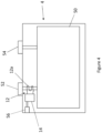
- Figures 4 and 5 shows examples of two ways in which the inductive current sensor 12 can be arranged to sense the primary current at a terminal of the DC link capacitor 4.
- Figure 4 shows the DC link capacitor 4, including a capacitor element 50, and capacitor terminals 52, 54.
- the coil 12a of the inductive current sensor 12 is wrapped freely around the capacitor terminal 52. This has the advantage that it can be easily installed in an existing system, and does not require any specialised components. However it is not very mechanically stable, and these components are expensive.
- the inductive current sensor 12 is then connected to the detection circuit 14, which is in turn connected to a harness connector 56, which enables connection of the over-current detection system to other parts of an electrical power converter.
- the capacitor 4 described in relation to Fig. 4 may find use in any application where it is beneficial to integrate a current sensing function into a capacitor, i.e. not only for detecting an over-current as described in relation to Figs. 1-3 .
- FIG. 5 shows an alternative example of an arrangement for the inductive current sensor 12.
- the capacitor is not shown in this Figure.
- the arrangement still includes the coil 12a of the inductive current sensor 12, the detection circuit 14, and the harness connector 56.
- the coil 12a is embedded within a printed circuit board 60, which also contains the detection circuit 14 and the harness connector 56.
- the printed circuit board 60 contains a hole, 62, sized so that the terminal of the capacitor 52 can be slid through the hole 62, thus positioning the embedded coil 12a around the capacitor terminal.
- This arrangement is very mechanically stable since the coil 12 is securely embedded within the PCB 60 and the PCB 60 is supported by the underlying capacitor.
- the PCB 60 may be mounted over a terminal of any suitable capacitor in order to add a current sensing function, i.e. not only in the over-current detection circuits described in relation to Figs. 1-3 .
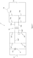
- FIGS 6 and 7 show some examples of alternative electrical power converters in which the described current detection arrangement can be implemented.
- FIG. 6 shows a single-phase DC-AC inverter 1' which is an H-bridge arrangement.
- the single-phase DC-AC inverter 1' includes a DC-link capacitor 4', connected in parallel to two pairs of semiconductor switches 2a', 2b'.
- the switches 2a', 2b' are switched in a known manner so that from a DC power source 3' an AC output is produced on the output load terminals 10a', 10b', which are connected between each pair of switches 2a', 2b'.
- Over-current detection is carried out using an inductive current sensor 12', in the same manner as described above with reference to the first example.
- FIG 7 shows an isolated DC-DC converter 1".
- the isolated DC-DC converter 1" includes a DC link capacitor 4", connected in parallel to two pairs of semiconductor switches 2a", 2b".
- the switches 2a", 2b" are switched in a known manner so that from a DC power source 3" an AC output is produced on the output load terminals 10a", 10b", which are connected between each pair of switches 2a", 2b".
- a transformer 70 is used to provide isolation between the input and output portions of the circuit 1".
- the transformer 70 connects to the output terminals 10a", 10b", and then the secondary portion of the transformer 70 connects to a rectifier portion of the DC-DC converter 1", which converts the AC output from the output terminals 10a", 10b" into DC current.
- the secondary part of the transformer 70 connects to input terminals 72a, 72b of the rectifier part of the DC-DC converter 1".
- the rectifier part of the circuit also includes two pairs of diodes 74a, 74b, connected in parallel, a capacitor 76, in parallel with the pairs of diodes and a transformer coil 78 in series with the capacitor. These function together to convert the AC output received from the first part of the converter into direct current.
- Over-current detection is carried out using an inductive current sensor 12", in the same manner as described above with reference to the first example.
Landscapes
- Engineering & Computer Science (AREA)
- Power Engineering (AREA)
- Physics & Mathematics (AREA)
- General Physics & Mathematics (AREA)
- Inverter Devices (AREA)
- Power Conversion In General (AREA)
Priority Applications (2)
| Application Number | Priority Date | Filing Date | Title |
|---|---|---|---|
| EP22275003.6A EP4210209A1 (fr) | 2022-01-10 | 2022-01-10 | Détection de courant dans des convertisseurs de puissance électrique |
| US18/093,685 US12500511B2 (en) | 2022-01-10 | 2023-01-05 | Capacitor embedded rogowski current detection |
Applications Claiming Priority (1)
| Application Number | Priority Date | Filing Date | Title |
|---|---|---|---|
| EP22275003.6A EP4210209A1 (fr) | 2022-01-10 | 2022-01-10 | Détection de courant dans des convertisseurs de puissance électrique |
Publications (1)
| Publication Number | Publication Date |
|---|---|
| EP4210209A1 true EP4210209A1 (fr) | 2023-07-12 |
Family
ID=79317019
Family Applications (1)
| Application Number | Title | Priority Date | Filing Date |
|---|---|---|---|
| EP22275003.6A Pending EP4210209A1 (fr) | 2022-01-10 | 2022-01-10 | Détection de courant dans des convertisseurs de puissance électrique |
Country Status (2)
| Country | Link |
|---|---|
| US (1) | US12500511B2 (fr) |
| EP (1) | EP4210209A1 (fr) |
Families Citing this family (2)
| Publication number | Priority date | Publication date | Assignee | Title |
|---|---|---|---|---|
| KR102822473B1 (ko) * | 2020-12-02 | 2025-06-19 | 현대모비스 주식회사 | 스위칭전류센싱시의 옵셋보상 장치 및 방법 |
| FR3162945A1 (fr) * | 2024-05-30 | 2025-12-05 | Safran Electrical & Power | Dispositif de capacité pour un système de génération électrique d’un aéronef et procédé associé |
Citations (3)
| Publication number | Priority date | Publication date | Assignee | Title |
|---|---|---|---|---|
| EP2166635A1 (fr) * | 2008-09-23 | 2010-03-24 | ABB Oy | Mesure du courant dans une unité d'inverseur et un convertisseur de fréquence |
| US20170104404A1 (en) * | 2015-10-07 | 2017-04-13 | Industrial Technology Research Institute | Protection circuit |
| JP2019221070A (ja) * | 2018-06-20 | 2019-12-26 | 新電元工業株式会社 | スイッチング電源装置 |
Family Cites Families (8)
| Publication number | Priority date | Publication date | Assignee | Title |
|---|---|---|---|---|
| US5815391A (en) | 1996-03-19 | 1998-09-29 | International Rectifier Corporation | Current sensing circuit for pulse width modulated motor drive |
| DE102004011023A1 (de) | 2004-03-04 | 2005-09-15 | Siemens Ag | Drei- oder vierpoliger Niederspannungs-Leistungsschalter mit als Stromsensoren dienenden Rogowskispulen |
| AT511807B1 (de) * | 2011-08-01 | 2013-03-15 | Univ Wien Tech | Verfahren und vorrichtung zur online-erkennung einer zustandsverschlechterung einer isolierung in einer elektrischen maschine |
| US9577421B2 (en) | 2015-06-18 | 2017-02-21 | General Electric Company | System and method for isolating ground faults in a wind turbine |
| WO2017197269A1 (fr) | 2016-05-13 | 2017-11-16 | The University Of North Carolina At Charlotte | Détection de courant de rogowski magnétorésistif sans contact à large bande |
| CN106849021A (zh) | 2017-03-17 | 2017-06-13 | 深圳市禾望电气股份有限公司 | 半导体开关过流检测方法及变流器 |
| EP3534538A1 (fr) | 2018-02-28 | 2019-09-04 | LEM Intellectual Property SA | Module de commande de commutateur de puissance électronique |
| US11114839B2 (en) | 2018-11-16 | 2021-09-07 | General Electric Company | System and method for mitigating overvoltage on a DC link of a power converter |
-
2022
- 2022-01-10 EP EP22275003.6A patent/EP4210209A1/fr active Pending
-
2023
- 2023-01-05 US US18/093,685 patent/US12500511B2/en active Active
Patent Citations (3)
| Publication number | Priority date | Publication date | Assignee | Title |
|---|---|---|---|---|
| EP2166635A1 (fr) * | 2008-09-23 | 2010-03-24 | ABB Oy | Mesure du courant dans une unité d'inverseur et un convertisseur de fréquence |
| US20170104404A1 (en) * | 2015-10-07 | 2017-04-13 | Industrial Technology Research Institute | Protection circuit |
| JP2019221070A (ja) * | 2018-06-20 | 2019-12-26 | 新電元工業株式会社 | スイッチング電源装置 |
Non-Patent Citations (1)
| Title |
|---|
| VOTZI HELMUT L ET AL: "Low-Cost Current Sensor for Power Capacitors Based on a PCB Rogowski-Coil", PCIM EUROPE 2011, 17 May 2011 (2011-05-17), pages 621 - 626, XP055930613, Retrieved from the Internet <URL:https://www.riccardofontanini.it/projects/rogowski/pdf/coilsplanar.pdf> [retrieved on 20220613] * |
Also Published As
| Publication number | Publication date |
|---|---|
| US20230223838A1 (en) | 2023-07-13 |
| US12500511B2 (en) | 2025-12-16 |
Similar Documents
| Publication | Publication Date | Title |
|---|---|---|
| US8760832B2 (en) | Load circuit protection device | |
| EP1811645B1 (fr) | Procede et appareil de protection de circuit d'alimentation electrique | |
| CN101868899B (zh) | 调光器电路中的过流保护 | |
| US5936387A (en) | Gate drive circuit for power converters that reduces surge voltages | |
| EP0792007B1 (fr) | Module de puissance universel | |
| KR100419324B1 (ko) | 전력공급장치를구비하는전자트립장치 | |
| US12500511B2 (en) | Capacitor embedded rogowski current detection | |
| CN117767226A (zh) | 具有集成固态断路器的可调速驱动及其操作方法 | |
| CN114982085B (zh) | 用于保护电负载免受过电压影响的方法和设备 | |
| CN113451995B (zh) | 一种短路和过流保护装置和方法 | |
| EP3539211A1 (fr) | Entraînement de moteur | |
| EP0992104B1 (fr) | Systeme d'eclairage basse tensi0n | |
| US20040090723A1 (en) | Method and system for providing power to circuit breakers | |
| US20080239767A1 (en) | Power supply circuit with pulse generating circuit and current-limiting circuit | |
| KR100781131B1 (ko) | 과전류/단락 계전기를 겸한 전자식무접점릴레이 | |
| CN209282822U (zh) | 控制电路和电子设备 | |
| CN117916969A (zh) | 用于保护电流馈电变换器免受过电压影响的方法 | |
| CN211428908U (zh) | 一种过流保护电路、变流器及供电网路 | |
| JP3713795B2 (ja) | 制御装置の出力回路 | |
| US11929666B2 (en) | Gate drive circuit and power conversion device | |
| JP3449172B2 (ja) | 3相4線中性線欠相検出装置及び回路遮断器 | |
| KR102785674B1 (ko) | 이중 과전류 보호기능을 갖는 SiC 소자를 이용한 ESS 통합형 UPS 및 과전류 이중 보호기법 | |
| US20250125607A1 (en) | Desaturation configurations for power devices | |
| US20250253642A1 (en) | Fault Detection Circuit for Solid-State Motor Controllers | |
| KR20250176792A (ko) | 이중 과전류 보호기능을 갖는 SiC 소자를 이용한 ESS 통합형 UPS 및 과전류 이중 보호기법 |
Legal Events
| Date | Code | Title | Description |
|---|---|---|---|
| PUAI | Public reference made under article 153(3) epc to a published international application that has entered the european phase |
Free format text: ORIGINAL CODE: 0009012 |
|
| STAA | Information on the status of an ep patent application or granted ep patent |
Free format text: STATUS: THE APPLICATION HAS BEEN PUBLISHED |
|
| AK | Designated contracting states |
Kind code of ref document: A1 Designated state(s): AL AT BE BG CH CY CZ DE DK EE ES FI FR GB GR HR HU IE IS IT LI LT LU LV MC MK MT NL NO PL PT RO RS SE SI SK SM TR |
|
| STAA | Information on the status of an ep patent application or granted ep patent |
Free format text: STATUS: REQUEST FOR EXAMINATION WAS MADE |
|
| 17P | Request for examination filed |
Effective date: 20240111 |
|
| RBV | Designated contracting states (corrected) |
Designated state(s): AL AT BE BG CH CY CZ DE DK EE ES FI FR GB GR HR HU IE IS IT LI LT LU LV MC MK MT NL NO PL PT RO RS SE SI SK SM TR |
|
| STAA | Information on the status of an ep patent application or granted ep patent |
Free format text: STATUS: EXAMINATION IS IN PROGRESS |
|
| 17Q | First examination report despatched |
Effective date: 20250210 |