EP4217207B1 - Procédé de fabrication d'un élément de sécurité optiquement variable - Google Patents
Procédé de fabrication d'un élément de sécurité optiquement variable Download PDFInfo
- Publication number
- EP4217207B1 EP4217207B1 EP21746642.4A EP21746642A EP4217207B1 EP 4217207 B1 EP4217207 B1 EP 4217207B1 EP 21746642 A EP21746642 A EP 21746642A EP 4217207 B1 EP4217207 B1 EP 4217207B1
- Authority
- EP
- European Patent Office
- Prior art keywords
- embossing
- layer
- coating
- varnish
- reflection
- Prior art date
- Legal status (The legal status is an assumption and is not a legal conclusion. Google has not performed a legal analysis and makes no representation as to the accuracy of the status listed.)
- Active
Links
Images



Classifications
-
- B—PERFORMING OPERATIONS; TRANSPORTING
- B42—BOOKBINDING; ALBUMS; FILES; SPECIAL PRINTED MATTER
- B42D—BOOKS; BOOK COVERS; LOOSE LEAVES; PRINTED MATTER CHARACTERISED BY IDENTIFICATION OR SECURITY FEATURES; PRINTED MATTER OF SPECIAL FORMAT OR STYLE NOT OTHERWISE PROVIDED FOR; DEVICES FOR USE THEREWITH AND NOT OTHERWISE PROVIDED FOR; MOVABLE-STRIP WRITING OR READING APPARATUS
- B42D25/00—Information-bearing cards or sheet-like structures characterised by identification or security features; Manufacture thereof
- B42D25/30—Identification or security features, e.g. for preventing forgery
- B42D25/324—Reliefs
-
- B—PERFORMING OPERATIONS; TRANSPORTING
- B42—BOOKBINDING; ALBUMS; FILES; SPECIAL PRINTED MATTER
- B42D—BOOKS; BOOK COVERS; LOOSE LEAVES; PRINTED MATTER CHARACTERISED BY IDENTIFICATION OR SECURITY FEATURES; PRINTED MATTER OF SPECIAL FORMAT OR STYLE NOT OTHERWISE PROVIDED FOR; DEVICES FOR USE THEREWITH AND NOT OTHERWISE PROVIDED FOR; MOVABLE-STRIP WRITING OR READING APPARATUS
- B42D25/00—Information-bearing cards or sheet-like structures characterised by identification or security features; Manufacture thereof
- B42D25/20—Information-bearing cards or sheet-like structures characterised by identification or security features; Manufacture thereof characterised by a particular use or purpose
- B42D25/29—Securities; Bank notes
-
- B—PERFORMING OPERATIONS; TRANSPORTING
- B42—BOOKBINDING; ALBUMS; FILES; SPECIAL PRINTED MATTER
- B42D—BOOKS; BOOK COVERS; LOOSE LEAVES; PRINTED MATTER CHARACTERISED BY IDENTIFICATION OR SECURITY FEATURES; PRINTED MATTER OF SPECIAL FORMAT OR STYLE NOT OTHERWISE PROVIDED FOR; DEVICES FOR USE THEREWITH AND NOT OTHERWISE PROVIDED FOR; MOVABLE-STRIP WRITING OR READING APPARATUS
- B42D25/00—Information-bearing cards or sheet-like structures characterised by identification or security features; Manufacture thereof
- B42D25/30—Identification or security features, e.g. for preventing forgery
- B42D25/351—Translucent or partly translucent parts, e.g. windows
-
- B—PERFORMING OPERATIONS; TRANSPORTING
- B42—BOOKBINDING; ALBUMS; FILES; SPECIAL PRINTED MATTER
- B42D—BOOKS; BOOK COVERS; LOOSE LEAVES; PRINTED MATTER CHARACTERISED BY IDENTIFICATION OR SECURITY FEATURES; PRINTED MATTER OF SPECIAL FORMAT OR STYLE NOT OTHERWISE PROVIDED FOR; DEVICES FOR USE THEREWITH AND NOT OTHERWISE PROVIDED FOR; MOVABLE-STRIP WRITING OR READING APPARATUS
- B42D25/00—Information-bearing cards or sheet-like structures characterised by identification or security features; Manufacture thereof
- B42D25/30—Identification or security features, e.g. for preventing forgery
- B42D25/36—Identification or security features, e.g. for preventing forgery comprising special materials
- B42D25/373—Metallic materials
-
- B—PERFORMING OPERATIONS; TRANSPORTING
- B42—BOOKBINDING; ALBUMS; FILES; SPECIAL PRINTED MATTER
- B42D—BOOKS; BOOK COVERS; LOOSE LEAVES; PRINTED MATTER CHARACTERISED BY IDENTIFICATION OR SECURITY FEATURES; PRINTED MATTER OF SPECIAL FORMAT OR STYLE NOT OTHERWISE PROVIDED FOR; DEVICES FOR USE THEREWITH AND NOT OTHERWISE PROVIDED FOR; MOVABLE-STRIP WRITING OR READING APPARATUS
- B42D25/00—Information-bearing cards or sheet-like structures characterised by identification or security features; Manufacture thereof
- B42D25/40—Manufacture
- B42D25/405—Marking
- B42D25/425—Marking by deformation, e.g. embossing
-
- B—PERFORMING OPERATIONS; TRANSPORTING
- B42—BOOKBINDING; ALBUMS; FILES; SPECIAL PRINTED MATTER
- B42D—BOOKS; BOOK COVERS; LOOSE LEAVES; PRINTED MATTER CHARACTERISED BY IDENTIFICATION OR SECURITY FEATURES; PRINTED MATTER OF SPECIAL FORMAT OR STYLE NOT OTHERWISE PROVIDED FOR; DEVICES FOR USE THEREWITH AND NOT OTHERWISE PROVIDED FOR; MOVABLE-STRIP WRITING OR READING APPARATUS
- B42D25/00—Information-bearing cards or sheet-like structures characterised by identification or security features; Manufacture thereof
- B42D25/40—Manufacture
- B42D25/405—Marking
- B42D25/43—Marking by removal of material
- B42D25/44—Marking by removal of material using mechanical means, e.g. engraving
-
- G—PHYSICS
- G02—OPTICS
- G02B—OPTICAL ELEMENTS, SYSTEMS OR APPARATUS
- G02B27/00—Optical systems or apparatus not provided for by any of the groups G02B1/00 - G02B26/00, G02B30/00
- G02B27/42—Diffraction optics, i.e. systems including a diffractive element being designed for providing a diffractive effect
- G02B27/4272—Diffraction optics, i.e. systems including a diffractive element being designed for providing a diffractive effect having plural diffractive elements positioned sequentially along the optical path
-
- G—PHYSICS
- G02—OPTICS
- G02B—OPTICAL ELEMENTS, SYSTEMS OR APPARATUS
- G02B5/00—Optical elements other than lenses
- G02B5/18—Diffraction gratings
- G02B5/1847—Manufacturing methods
- G02B5/1852—Manufacturing methods using mechanical means, e.g. ruling with diamond tool, moulding
-
- G—PHYSICS
- G02—OPTICS
- G02B—OPTICAL ELEMENTS, SYSTEMS OR APPARATUS
- G02B5/00—Optical elements other than lenses
- G02B5/18—Diffraction gratings
- G02B5/1861—Reflection gratings characterised by their structure, e.g. step profile, contours of substrate or grooves, pitch variations, materials
Definitions
- the invention relates to a method for producing an optically variable security element.
- Data storage media such as valuables or identification documents, but also other valuable items such as branded goods, are often provided with security elements for security purposes. These allow the authenticity of the data storage media to be verified and also serve as protection against unauthorized reproduction.
- the security elements can, for example, be in the form of a security thread embedded in a banknote, a cover film for a banknote with a hole, an applied security strip, a self-supporting transfer element or in the form of a feature area printed directly on a value document.
- Security elements with a viewing angle-dependent or three-dimensional appearance play a special role in authenticity assurance, as these cannot be reproduced even with the most modern copying machines.
- the security elements are equipped with optically variable elements that give the viewer a different image impression at different viewing angles and, for example, show a different color or brightness impression and/or a different graphic motif depending on the viewing angle.
- optically variable effects are described as, for example, movement effects, pump effects, depth effects or flip effects, which are realized with the help of holograms, microlenses or micromirrors.
- optically variable security elements were proposed that have two relief structures arranged at different heights and each provided with a colour coating (see WO 2020/011390 A1 , WO 2020/011391 A1 and WO 2020/011391 A2
- the colour coating of the higher relief structure is either structured as a grid or provided with recesses, so that when the security element is viewed at certain angles, the The colour of the paint coating of the deeper relief structure appears in the gaps between the grids or recesses.
- embossed lacquer layer is only applied to a production substrate in certain areas, the embossed lacquer layer is embossed - for example with a hologram structure - and metallized over the entire surface.
- the metallization is removed again in certain areas by selectively applying another layer - before or after metallization.
- the resulting security element is then removed from the production substrate.
- EP 3 216 620 A1 relates to a security element with a plurality of reflective facets, some of which have a random orientation and some of which have an orientation for reflection in an angular range.
- WO 2020/126077 A2 describes a method for producing an optically variable security element in which a non-metal coating is selectively lifted off from a higher relief structure.
- EP 2 996 885 B1 shows the preamble of claim 1.
- the invention is based on the object of specifying a robust method for producing optically variable security elements, in particular optically variable security elements with two independently selectable colors of the relief structures.
- a production carrier in the method for producing an optically variable security element, whose surface extension defines a z-axis perpendicular thereto.
- a first embossed lacquer layer is applied to the surface of the production carrier only in partial areas, so that lacquer areas with an embossed lacquer layer and free areas without an embossed lacquer layer are created in the surface area.
- the applied first embossed lacquer layer is provided with a first embossing at a first height level.
- the surface area is provided with a first coating in the free areas and in the painted areas.
- the surface area is also provided with a further layer in the free areas and optionally also in the painted areas. In the free areas, the first coating is removed again.
- the production carrier is removed according to the invention.
- the further layer is a second embossing lacquer layer, which is provided with a second embossing - at a second height level spaced from the first height level in the z-direction - so that a combination structure with the two embossings at two height levels is created.
- the first embossing lacquer layer prevents the first coating from being removed in the lacquer areas during or after the production carrier is removed from the combination structure. In the free areas, however, the first coating is removed during or after the production carrier is removed. In the free areas, the first coating is preferably removed with the production carrier and thus when the production carrier is removed removed.
- the first coating can have a higher adhesion to the production carrier than the first embossing lacquer layer to the production carrier.
- the first coating can have a higher adhesion to the production carrier than the first coating to an intermediate layer remaining in the combination structure, which can in particular be the second embossing lacquer layer, an adhesive layer or a dielectric layer.
- the first embossed lacquer layer remains in the combination structure when the production carrier is removed, particularly since it has a lower adhesion to the production carrier than the first coating.
- the removal of the first coating in the free areas can alternatively or additionally also take place after the production carrier has been removed.
- the first coating or a residue of the first coating that remains after removal is then removed by etching.
- the intermediate layer remaining in the combination structure can advantageously have a higher resistance to an etchant than the first coating. Since it usually has a higher layer thickness than the first coating, a similar or slightly lower resistance is theoretically also usable.
- the first embossing lacquer layer preferably prevents the removal of the first coating even after the production carrier has been removed. It can optionally have a higher resistance to an etchant than the first coating. However, since the embossing lacquer layer has a higher layer thickness than the first coating, a similar or slightly lower resistance is theoretically also usable.
- the first embossed lacquer layer lies directly on the surface of the production carrier, while in the free areas the first coating lies directly on the surface of the production carrier.
- the first coating lies with one side directly on the embossed surface of the first embossed lacquer layer.
- the intermediate layer can be, for example, the second embossed lacquer layer, an adhesive layer or a dielectric layer.
- the adhesions mentioned preferably differ by at least a factor of 2, more preferably at least a factor of 3 or 5, in particular at least a factor of 10.
- the adhesion of the first coating to the production carrier is more than a factor of 2 (3, 5 or 10) greater than the adhesion of the first embossing lacquer layer to the production carrier.
- the adhesion of the first coating to the production carrier is more than a factor of 2 (3 or 5) greater than the adhesion of the first coating to the intermediate layer remaining in the combination structure.
- the adhesion of the first coating to the intermediate layer is generally chosen to be greater than the adhesion of the embossing lacquer layer to the production carrier.
- the first coating is preferably a (first) reflection-enhancing coating which follows the first embossing; preferably a second reflection-enhancing coating follows the second embossing.
- first and/or second reflection-enhancing coating follow their embossing.
- the combination structure should comprise a first and a second relief structure with different colors, preferably reflective and/or transmissive.
- the first and second relief structures are formed by the first and second embossed lacquer layers, the first and second reflection-enhancing layers, and an optional first and second color layer.
- a product carrier of the combination structure is applied in one method step.
- at least the first embossing lacquer layer is arranged between the product carrier and the production carrier.
- the product carrier can be an end product carrier that forms part of the optically variable security element.
- the product carrier is a transfer product carrier on which the optically variable security element with its combination structure is arranged detachably (i.e. only temporarily). The security element remains temporarily on the transfer product carrier, for example until a transfer from the transfer product carrier to an object to be secured.
- the second embossing lacquer layer is applied and only provided with the second embossing on the production carrier.
- an already embossed second embossing lacquer layer is applied, in particular by means of an adhesive layer.
- the second embossing lacquer layer can follow the second embossing with its first surface and follow the first embossing with its second surface. If, however, a - for example colored - If an intermediate layer is applied in the lacquer areas (and the free areas) which compensates for the first embossing, the second embossing lacquer layer with the second surface does not follow the first embossing. Additionally or alternatively, the embossed second embossing lacquer layer can be provided with the second reflection-enhancing coating. Additionally or alternatively, a product carrier can be provided and connected to the, in particular coated, embossed second embossing lacquer layer by means of an adhesive layer.
- the second embossed lacquer layer on the product carrier can be provided with the second embossing beforehand.
- the embossed second embossed lacquer layer can be provided with the second reflection-enhancing coating beforehand.
- the adhesive layer can follow the second embossing with a first surface and follow the first embossing with the second surface. If, however, an intermediate layer - for example a colored one - is applied beforehand in the lacquer areas (and the free areas) which compensates for the first embossing, the adhesive layer with the second surface does not follow the first embossing. The same applies if the embossed second lacquer layer and the adhesive layer are arranged on different sides of the product carrier.
- the two relief structures can differ in terms of effect type and/or viewing angle range.
- the effect of the two relief structures from the given viewing side should differ in color for the viewer.
- the first, preferably reflection-increasing, coating and/or the second reflection-increasing coating is a reflection-increasing color coating.
- the reflection-increasing color coating can be formed by just one layer, such as a colored metallization or by a color-imparting HRI layer, or by a multi-layer structure.
- the reflection-increasing color coating can be only reflective or transmissive and color-effective in a reflective manner.
- it can be formed by a color-imparting (transmissive and reflective) HRI multi-layer structure, by a color-shifting multi-layer structure (usually with 3 layers of absorber, dielectric and reflector, for example with a full-surface or partial reflector) or a color-filtering, transmissive and reflective multi-layer structure (usually with 3 layers of absorber, dielectric and absorber).
- a color-imparting (transmissive and reflective) HRI multi-layer structure usually with 3 layers of absorber, dielectric and reflector, for example with a full-surface or partial reflector
- a color-filtering, transmissive and reflective multi-layer structure usually with 3 layers of absorber, dielectric and absorber.
- it is formed by a reflection-enhancing partial layer which is provided with a partial layer of translucent and/or luminescent paint.
- the first coating which is a reflection-enhancing coating, and/or the second reflection-enhancing coating, have a color-reflective effect due to a substructure of their embossing, in particular a subwavelength structure, interference structure (for example as a nanostructure with a binary surface) or diffraction structure.
- a first or second translucent color layer is provided, or a first or second color-imparting multilayer substructure (such as dielectric and reflector/absorber) is provided, which only has a colored effect in a reflective and/or transmissive manner together with the reflection-increasing coating.
- a first or second translucent The color layer can also be designed as an unstructured color layer, which means that neither of its sides follows either of the two embossings.
- the same variant is used for both embossings of the combination structure.
- two different ones of the three variants mentioned can be used in one security element.
- the first coating and/or the second reflection-enhancing coating is particularly preferably a vapor-deposited layer, in particular a metal layer or an HRI layer.
- the first and/or second embossed structure is advantageously formed in a transparent or translucently colored embossed lacquer layer. If an embossed lacquer layer is arranged between the viewer and the first and/or second reflection-enhancing coating, the coloring of the embossed lacquer layer can determine the color effect or modify a color effect of the first or second reflection-enhancing coating. When using transparent, i.e. uncolored, embossed lacquer layers, the color effect of the embossed structures is determined by the respective color coating or color layer. By using translucently colored embossed lacquer layers, the color effect of the color coating can be modified, so that, for example, different color effects of the embossed lacquer layers can be created despite using the same metallization, for example an Al metallization.
- the lacquer areas and free areas are formed at least in a partial area of the surface area as a regular or irregular grid with grid elements and grid spaces, wherein the dimensions of the grid elements and/or the The dimensions of the grid spaces in one or both lateral directions are below 140 ⁇ m, preferably between 20 ⁇ m and 100 ⁇ m, in particular between 20 ⁇ m and 60 ⁇ m. The viewer does not perceive the grid.
- the dimensions of the grid elements or grid spaces are selected in particular so that they are below the resolution of the human eye.
- the security element advantageously displays an appearance when tilted or the viewing direction changes accordingly, which suddenly jumps from a first to a second appearance (or from the second to the first appearance when tilted back).
- the motif shown for example, value number or coat of arms
- the color for example, yellow or blue
- a binary color, motif and effect change is possible, especially since an optically variable effect of the motifs (flat/three-dimensional and/or lying in the substrate plane/floating above the substrate plane/floating below the substrate plane and/or stationary/moving ...) can also differ.
- the grid formed by the lacquer areas and free areas is advantageously designed with a constant area coverage by the grid elements, which is expediently between 30% and 70%, preferably between 40% and 60%, in particular about 50%.
- the lacquer areas and free areas are formed as an effect area at least in a partial area of the surface area, in which the lacquer areas and/or the free areas have lateral dimensions of more than 140 ⁇ m.
- the effect area is large enough to be perceived separately by the observer.
- the security element preferably shows two different effects (for example a three-dimensional motif and a movement effect such as a moving bar), which appear in two different colors.
- the areas with different color impressions and different effects are precisely matched to one another, which is also referred to below as color-to-effect matching.
- At least one lacquer region and/or at least one free region is formed with lateral dimensions of more than 250 ⁇ m, preferably of more than 500 ⁇ m and in particular of more than 1 mm.
- the embossed structures are advantageously formed by micromirror arrangements with directed micromirrors.
- the micromirrors are formed in particular by non-diffractive mirrors and do not produce any color separation. Plane mirrors, concave mirrors and/or Fresnel-like mirrors can preferably be used.
- the lateral dimensions of the micromirrors are expediently below 50 ⁇ m, advantageously below 20 ⁇ m, preferably around 10 ⁇ m, i.e. between 7 ⁇ m and 13 ⁇ m. On the other hand, the lateral dimensions of the micromirrors are also above 2 ⁇ m, in particular above 3 ⁇ m or even above 5 ⁇ m.
- the pitch of the micromirrors is preferably less than 10 ⁇ m, preferably less than 5 ⁇ m.
- embossed relief structures in particular Fresnel lenses, concave mirrors, hologram structures, nanostructures or diffractive blazed gratings, can be used instead of micromirrors.
- Achromatic diffraction gratings so-called matt structures, can be used particularly advantageously here, as they essentially reflect white light and thus do not disturb the color effect of the coating or any color layers by generating diffraction colors.
- the relief structures can also have subwavelength structures, in particular subwavelength gratings, which, in combination with the respective reflection-enhancing coating, determine or at least help determine its color.
- the first and second color coatings completely cover the respective embossed structure. If an embossed structure, such as the first embossed structure, is only present in partial areas of the surface area, complete coverage of the embossed structure refers to the complete coverage of those partial areas in which the embossed structure is present in the surface area.
- negative markings can be provided in the security element through recesses in the first and/or second reflection-enhancing coating, which can form, for example, text, symbols or value numbers.
- transmissive negative markings can be formed, which form, for example, text, symbols or value numbers. This is particularly This is possible by creating congruent recesses in the first and second reflection-enhancing coatings in the painted areas and/or by creating recesses in the second reflection-enhancing coating in the free areas.
- Negative marks can be provided in the grid areas formed by the above-mentioned lacquer areas and free areas. However, they usually appear less visually attractive there, since the line thickness of the negative marks is usually greater than the grid of the first embossed lacquer layer, so that the viewer may be able to see the printing grid of the negative marks.
- Transparent colorless negative markings require that both embossing lacquer layers (first process variant) or the first embossing lacquer layer and the laminating adhesive (second process variant) are colorless. If one or both embossing lacquer layers or the laminating adhesive are transparent colored, colored negative markings result with the color effect of the colored layers or the subtractive color effect of both colored layers. b) The negative marks can be created in the free areas of the surface area where only the second embossing lacquer layer is present. In this case, maintaining the register is easier because only the reflection-enhancing coating of the second relief structure needs to be removed/demetallized.
- Transparent, colorless negative markings require that the color effect of the second embossed structure is created by a metal layer that is removed in the recesses. If the second embossed lacquer layer (first process variant) or the laminating adhesive (second process variant) is colored in a translucent manner, colored negative markings are produced.
- both embossed structures are constructed on the same side of the production carrier or the end product carrier in order to have as few work steps as possible in the manufacture of the security element and to reliably achieve the desired visual effects.
- the described reflective surface area of the security element can be combined with other security features, for example with holograms, in particular true-colour holograms, with sub-wavelength gratings or other sub-wavelength structures, with micro-mirror arrangements without diffractive gratings, or with security features based on special material properties, such as electrical conductivity, magnetic Properties, luminescence, fluorescence or the like, as are known from the prior art.
- the optically variable security element can be provided with further layers, such as a protective, covering or additional functional layer, a primer layer or a heat-sealing lacquer layer.
- a protective, covering or additional functional layer such as a primer layer or a heat-sealing lacquer layer.
- FIG. 1 shows a schematic representation of a banknote 10 with an optically variable security element 12 produced according to the invention in the form of an adhesive-bonded transfer element. It is understood, however, that the invention is not limited to transfer elements and banknotes, but can be used for all types of security elements, for example for labels on goods and packaging or for securing documents, ID cards, passports, credit cards, health cards and the like. In the case of banknotes and similar documents, in addition to transfer elements (such as patches with or without their own carrier layer), security threads or security strips can also be used.
- the security element 12 itself is very flat, but nevertheless gives the viewer the three-dimensional impression of a motif 14 that appears to bulge out of the plane of the banknote 10 and appears in a first color.
- the motif 14 can, for example, a value number, a portrait or another graphic motif.
- a movement effect in a second color is visible in a partial area 16.
- a light bar can move back and forth along the curved partial area 16 and create a so-called rolling bar effect.
- the areas of different colors (first and second colors) and different effects (three-dimensional motif or moving bar) are precisely aligned with one another. This alignment is also referred to below as color-to-effect alignment.
- the security element 12 contains with reference to the cross section of the Fig. 2 a flat end product carrier 18, the surface area of which defines an xy plane and a z axis perpendicular to it.
- a multi-colored reflective surface area 20 is arranged on the end product carrier 18, which contains two embossed structure areas 24, 34 that are arranged in the z direction at two specific, different heights relative to the flat carrier 18.
- the different heights of the embossed structure areas 24, 34 are defined in the exemplary embodiment by the different heights of the base areas of the micromirror arrangements 24, 34 above the carrier 18.
- the two embossed structure areas each represent micromirror embossings or micromirror arrangements 24, 34, which are formed from a large number of micromirrors inclined relative to the xy plane.
- the local angles of inclination of the micromirrors are selected such that the relief structure of the micromirror arrangements 24, 34 together with the respective color coating produce a desired optical appearance, such as the curved three-dimensional impression of the motif 14 or the rolling bar effect of the partial area 16.
- the micromirror arrangements 24, 34 are each provided with a reflection-enhancing color coating 26, 36, which creates the different color impression of the micromirror arrangements in reflection for an observer.
- the micromirror arrangements 24, 34 are coated with metals 26, 36 that reflect in different colors, for example aluminum and copper.
- the different color impression can also be formed in another way, for example by combining a metallization (for example made of aluminum or silver) that reflects essentially evenly across the entire visible spectral range with a translucent color, as explained in more detail elsewhere.
- the micromirror arrangements 24, 34 each represent embossed structures that are embossed into a previously applied embossed lacquer layer 22, 32.
- the embossed lacquer layers 22, 32 can be colorless, transparent or colored.
- the security element 12 is designed for viewing from above (or in reflection), in this case from the side facing away from the carrier 18.
- the micromirror arrangement 24 further away from the observer is therefore also referred to as the lower micromirror arrangement and the micromirror arrangement 34 closer to the observer is referred to as the higher micromirror arrangement.
- the two micromirror arrangements 24, 34 of the embodiment are arranged one above the other, with the higher micromirror arrangement 34 having at least one large-area recess 42, for example in Form of a 5 mm wide and 2 cm long curved strip ( Fig.1 ).
- the observer looks at the lower micromirror arrangement 24 with its color coating 26, while the visual impression of the surface area 20 in the area 44 outside the recess 42 is determined by the higher micromirror arrangement 34 with the color coating 36.
- the observer When viewing the security element 12 in reflection, the observer perceives the motif 14 generated by the micromirror arrangement 34 in the areas 44 outside the recess 42 with a first color that is determined by the color of the color coating 36 and the color or colorlessness of the embossed lacquer layer 32.
- a movement effect occurs within the recess 42, in which, for example, when the banknote 10 is tilted, a bright bar of a second colour appears within the curved partial area 16 ( Fig.1 ) appears to run back and forth.
- the second color is determined by the color of the color coating 26 and the color or colorlessness of the embossed lacquer layer 22.
- the height difference between the two micromirror arrangements 24, 34 is in the range of a few micrometers or a few tens of micrometers and is therefore not perceptible to the viewer.
- the two differently colored motifs and the different effects 14, 16 therefore appear to the viewer to be arranged in exact register with one another.
- a production carrier 30 is provided, the surface of which has a low adhesion to embossing lacquer and a high adhesion to metal.
- the surface area of the production carrier 30 defines an xy plane and a z axis perpendicular to it.
- the production carrier 30 is preferably a plastic film. In particular, it has a smooth surface or a surface with reduced adhesion.
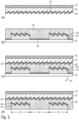
- a first embossing lacquer layer 32 is applied to its surface in the desired partial areas and a first embossing in the form of the desired micromirror embossing 34 is embossed into the embossing lacquer layer 32, as in Fig. 3b shown.
- lacquer areas 52 with an embossed embossed lacquer layer 32, 34 and free areas 54 without an embossed lacquer layer are thereby produced, the free areas 54 corresponding to the desired recesses 42 in the finished security element ( Fig. 2 ) and the lacquer areas 52 correspond to the desired areas 44 outside the recesses 42.
- the wetting properties of the embossing lacquer are selected or adjusted accordingly both on the production carrier 30 and on the embossing tool itself (not shown).
- the embossing lacquer layer 32 can be applied in particular by means of screen printing, offset printing, flexographic printing or gravure printing.
- UV lacquer, a thermoplastic lacquer or a dual cure system, i.e. a combination of UV embossing lacquer and thermoplastic lacquer, can be used as the embossing lacquer.
- the surface area 20 is metallized over the entire surface, for example with an aluminum layer.
- the metallization is preferably carried out by vapor deposition (PVD, CVD).
- PVD vapor deposition
- the metal layer 36 is applied in the free areas 54 on the surface of the production carrier 30, and in the lacquer areas 52 on the first embossed embossing lacquer layer 32, 34, so that a first reflective embossed structure is created in the lacquer areas 52 at a first height level H1, as in Fig.
- the printed and/or cured first embossing lacquer layer 32 in the lacquer region 52 adheres approximately 10 times worse to the production carrier 30 than the vapor-deposited first reflection-enhancing layer 36 (4 to 8 N/m compared to 50 to 90 N/m).
- the structure formed in this way in the surface region 20 is referred to here as the primary structure, which is subsequently supplemented with a structure referred to as the secondary structure, which in turn has a second, embossed and metallized embossing lacquer layer located inside the finished product and an external (end) product carrier.
- a full-surface second embossing lacquer layer 22 is applied to the primary structure of the Fig. 3(c) applied, as in Fig. 4(a) shown, and this second embossing lacquer layer 22 is then provided with the second embossing in the form of the desired micromirror embossing 24, as shown in Fig. 4(b) shown.
- the surface area 20 is again metallized over its entire surface, for example with a copper layer, and thereby a second metal layer 26 is applied over its entire surface to the embossed second embossing lacquer layer 22, 24, so that that a second reflective embossed structure is created at a second height level H2, as in Fig. 4(c) shown.
- the final product carrier 18 is provided and bonded to the metallized embossing lacquer layer 22 by means of an adhesive layer 19, as shown in Fig. 4(d)
- the end product carrier 18 and the adhesive layer 19 are selected such that the adhesion between the target substrate 18, the adhesive layer 19 and the metallization 26 is greater than the adhesion between the production carrier 30 and the embossing lacquer layer 32 or metallization 36.
- the production carrier 30 is subtracted from the combination structure thus formed 56, see Fig. 4(d) . Due to the high adhesion of the production carrier 30 to the vapor-deposited metal and the low adhesion of the production carrier to the embossing lacquer, the metal lying in the free areas 54 is removed together with the production carrier during stripping 56, while the embossing lacquer 32 and thus also its metallization 36 remain in the lacquer areas 52 in the combination structure, as in Fig. 4(e) The embossing lacquer 32 of the lacquer areas 52 thus forms a lifting protection for the embossing lacquer metallization and ensures partial demetallization of the metal layer 36 only in the free areas 54.
- an optional etching step is carried out in which any metal residues on the exposed surface are removed.
- the first reflection-enhancing coating 36 has so far been described as a colored metal layer, which is therefore also referred to as a colored coating.
- the reflection-enhancing coating(s) 36 (36,26) can - as already indicated in this and in the other embodiments - can also be designed differently.
- a color-imparting HRI layer can also be used.
- the (or one of the) reflection-enhancing coatings 26, 36 can be formed by an achromatic reflection-enhancing partial layer, such as a metal layer or HRI layer, and a translucent color partial layer (seen from the viewer - lying above it).
- a first reflection-enhancing layer only produces a color effect together with other layers.
- the production carrier is removed, at least one of the other layers remains in the combination structure with its two embossed structures.
- one of the other layers is not removed when the first reflection-enhancing layer is removed by etching.
- the further layers would lie (in the free areas 54 and the lacquer areas 52) on the first reflection-enhancing layer 36, in Fig. 4c i.e. between the first reflection-increasing layer 36 and the second embossing lacquer layer 22.
- the first reflection-increasing layer can serve as a reflector or as an absorber of a color-imparting multilayer structure, which produces a color effect, for example as an absorber-dielectric-absorber or reflector-dielectric-absorber.
- the reflection-increasing layer could also be an HRI layer of a color-imparting refractive index-based multilayer structure, which consists of transparent sublayers with different refractive indices.
- first and/or the second relief structure of the combination structure could - in all embodiments also of the other figures, which in turn also comprise color-imparting embossing lacquer or adhesive layers - be achieved in one of the ways mentioned or in different ways of the ways mentioned.
- etching step may be mandatory in other embodiments in which the metal layer 36 remains on the embossing lacquer in the free areas 54 during removal.
- the reflection-enhancing layer in the free areas is only removed by etching.
- the surface exposed by removing the production carrier 30 can be coated with a protective lacquer layer 48 ( Fig. 2 ) or a thin, transparent (PET) film can be laminated on.
- a protective lacquer layer 48 Fig. 2
- PET thin, transparent
- further known production steps can be carried out to complete the process, such as coating with a hot-seal varnish.
- the terms “deeper relief structure” and “higher relief structure” refer to the position of the relief structures in the finished security element ( Fig. 2 ) relative to an observer. The designations therefore do not reflect the order in which the relief structures are applied during production. Since the security element is designed in particular to be viewed from the side of the production carrier that is later removed, the described production First, the (later) higher relief structure is created on the production carrier and then the (later) lower relief structure is created on top of that.
- a final product carrier 18 is first provided and printed over the entire surface with a second embossing lacquer layer 22.
- the second embossing lacquer layer 22 is then provided with the second embossing in the form of the desired micromirror embossing 24 and metallized over the entire surface, for example with a copper layer, in order to apply the second metal layer 26, as in Fig. 5(a) shown.
- a laminating varnish 60 is applied to the metallization 36 of the production carrier 30 or to the metallization 26 of the end product carrier 18 or to both metallizations 26, 36.
- the laminating varnish can be clear transparent or colored transparent.
- Fig. 5(b) As an example, the variant of applying the laminating varnish 60 only to the metallization 36 of the production carrier 30 is shown.
- the production carrier 30 can in particular be provided with a roughened surface so that the upper surface of the metallization 36 to the laminating lacquer 60 is smoother than the lower surface of the metallization 36.
- the production carrier 30 is subtracted 56 from the combination structure thus formed, as in Fig. 5(c) shown. Due to the high adhesion of the production carrier 30 to metal and the low adhesion of the production carrier to embossing lacquer, the metal lying in the free areas 54 is removed together with the production carrier during stripping 56, while the embossing lacquer 32 and thus also its metallization 36 remain in the lacquer areas 52 in the combination structure, as shown in Fig. 5(d) shown. The embossing lacquer 32 of the lacquer areas 52 also forms a lifting protection for the embossing lacquer metallization in this process variant and ensures partial demetallization of the metal layer 36 only in the free areas 54.
- an etching step can also be carried out after the removal of the production carrier 30.
- this etching step in the embodiment according to Fig.5 Any metal residues on the exposed surface must be removed. Analogous to Fig.4 However, in other designs with laminating adhesive, removal of the first reflection-enhancing layer would only be conceivable by etching.
- the surface exposed by removing the production carrier 30 can be further coated with a protective lacquer layer to improve the circulation resistance of the security element, or a thin, transparent (PET) film can be laminated on.
- a protective lacquer layer to improve the circulation resistance of the security element
- PET thin, transparent film
- the designs described can be provided with negative markings for additional security, for example in the form of text, symbols or value numbers.
- the negative markings are intended for viewing in a transparent manner.
- Figure 6 shows a security element 70 which, like the security element of the Fig. 2 according to the first process variant, but with additional negative markings 72, 74.
- the first negative markings 72 are provided in the free areas 54 of the surface area 20, in which only the second embossed structure 22, 24, 26 is present, and are formed by a partial demetallization of the second color coating 26. If the second embossed lacquer layer 22 is colorless transparent, the negative markings 72 also appear colorless transparent, while in the case of a colored second embossed lacquer layer 22, the negative markings 72 appear with the transparent color of the embossed lacquer layer 22.
- the second negative markings 74 are provided in the lacquer areas 52 of the surface area 20 in which the two embossed structures overlap, and are formed by a partial demetallization of both the first color coating 36 and the second color coating 26. If both embossed lacquer layers 22, 32 are colorless transparent, the negative markings 74 also appear colorless transparent. If one of the two embossed lacquer layers 22, 32 is colored and the other is colorless transparent, the negative markings 74 appear with the transparent color of the colored embossed lacquer layer. If both embossed lacquer layers 22, 32 are colored, the negative markings 74 with a transparent colour which results from subtractive colour mixing of the colours of the embossing lacquer layers 22, 32.
- Figure 7 shows a security element 80 which is produced according to the second method variant of Fig.5 , but with additional negative markings 82, 84.
- the first negative markings 82 are provided in the free areas 54 of the surface area 20, in which only the second embossed structure 22, 24, 26 is present, and are formed by a partial demetallization of the second color coating 26. If the laminating varnish 60 is colorless transparent, the negative markings 82 also appear colorless transparent. In the case of a colored laminating varnish 60, the negative markings 82 appear with the transparent color of the laminating varnish 60.
- the second negative markings 84 are provided in the lacquer regions 52 of the surface region 20 in which the two embossed structures overlap, and are formed by a partial demetallization of both the first color coating 36 and the second color coating 26. If the embossing lacquer layer 32 and the laminating lacquer 60 are colorlessly transparent, the negative markings 84 also appear colorlessly transparent. If one of the two layers (embossing lacquer layer 32, laminating lacquer 60) is colored and the other is colorlessly transparent, the negative markings 84 appear with the transparent color of the colored layer. If both the embossing lacquer layer 32 and the laminating lacquer 60 are colored, the negative markings 84 appear with a transparent color that results from subtractive color mixing of the colors of the two layers 32, 60.
Landscapes
- Physics & Mathematics (AREA)
- Engineering & Computer Science (AREA)
- Manufacturing & Machinery (AREA)
- General Physics & Mathematics (AREA)
- Optics & Photonics (AREA)
- Business, Economics & Management (AREA)
- Accounting & Taxation (AREA)
- Finance (AREA)
- Mechanical Engineering (AREA)
- Credit Cards Or The Like (AREA)
Claims (15)
- Procédé de fabrication d'un élément de sécurité optiquement variable (12), procédé dans lequel- un support de production (30) est prévu dont l'étendue de surface définit un axe z perpendiculaire à celui-ci ;- dans une zone de surface (20), une première couche de vernis de gaufrage (32) est appliquée sur la surface du support de production uniquement par sous-zones, de sorte que les zones de vernis (52) pourvue d'une couche de vernis de gaufrage et les zones libres (54) sans couche de vernis gaufrée sont générées dans la zone de surface ;- la première couche de vernis de gaufrage appliquée (32) est pourvue d'un premier gaufrage (34) à un premier niveau en hauteur ;- la zone de surface (20) est pourvue d'un premier revêtement (36) dans les zones libres (54) et dans les zones de vernis (52) ;- la zone de surface (20) est pourvue d'une couche supplémentaire dans les zones libres (54) et éventuellement dans les zones de vernis (52) ; et- le premier revêtement (36) est à nouveau enlevé dans les zones libres (54) ;
caractérisé en ce que- le support de production (30) est retiré ;- la couche supplémentaire est une deuxième couche de vernis de gaufrage (22) qui est pourvue d'un deuxième gaufrage (24) à un deuxième niveau en hauteur distant du premier niveau en hauteur dans la direction z de sorte qu'une structure combinée comprenant les deux gaufrages (34, 24) est générée sur deux niveaux en hauteur ; et- la première couche de vernis de gaufrage (32) empêche l'élimination du premier revêtement (36) dans les zones de vernis (52) pendant ou après le retrait du support de production (30) de la structure combinée. - Procédé selon la revendication 1, caractérisé en ce quedans les zones de vernis (52), la première couche de vernis de gaufrage (32) reste dans la structure combinée lors du retrait du support de production (30), en particulier parce qu'elle présente une adhérence moindre au support de production (30) que le premier revêtement (36) ; et/oudans les zones libres (54), le premier revêtement (36) est retiré avec le support de production (30) et ainsi est enlevé, en particulier parce que le premier revêtement (36) présente une adhérence plus élevée au support de production (30) que celle de la couche de vernis de gaufrage (32) au support de production (30) et/ou que celle du premier revêtement (36) à la deuxième couche de vernis de gaufrage (22).
- Procédé selon la revendication 1 ou 2, caractérisé en ce quedans les zones de vernis (52), la première couche de vernis de gaufrage (32) empêche l'enlèvement du premier revêtement (36) après le retrait du support de production, notamment du fait qu'elle a une résistance plus élevée à un agent d'attaque chimique que le premier revêtement (36) ; et/oudans les zones libres (54), après le retrait du support de production, le premier revêtement (36) ou un reste du premier revêtement (36) est éliminé par attaque chimique.
- Procédé selon l'une des revendications 1 à 3, caractérisé en ce que le premier revêtement (36) est un revêtement d'augmentation de réflexion qui fait suite au premier gaufrage (34) ; de préférence, un deuxième revêtement d'augmentation de réflexion (26) faisant suite au deuxième gaufrage (24).
- Procédé selon l'une des revendications 1 à 4, caractérisé en ce que la structure combinée comprend une première et une deuxième structure en relief (32, 36 ; 22, 26) de couleurs différentes, de préférence réfléchissantes, notamment chacune étant formée par une première et une deuxième couche de vernis de gaufrage, la première ou la deuxième couche d'augmentation de réflexion et une couche de couleur facultative.
- Procédé selon l'une des revendications 1 à 5, caractérisé en ce qu'un support de produit (18) de la structure combinée (24, 34) est appliqué, de préférence au moins la première couche de vernis de gaufrage (32), en particulier uniquement la première couche de vernis de gaufrage ou les deux couches de vernis gaufrées (32, 22), est disposée entre le support de produit (18) et le support de production (30).
- Procédé selon la revendication 6, caractérisé en ce que le support de produit (18) est un support de produit final qui fait partie de l'élément de sécurité optiquement variable (12), ou le support de produit (18) est un support de produit de transfert sur lequel l'élément de sécurité optiquement variable (12) est disposé de manière amovible.
- Procédé selon l'une des revendications 1 à 7, caractérisé en ce que la deuxième couche de vernis de gaufrage (22) est appliquée puis pourvue du deuxième gaufrage (24) ; de préférencela deuxième couche de vernis de gaufrage (22) faisant suite au deuxième gaufrage (24) avec une surface et au premier gaufrage (34) avec la deuxième surface, et/oula deuxième couche de vernis de gaufrage étant pourvue du deuxième revêtement d'augmentation de réflexion, et/ouun support de produit (18) étant prévu qui est relié par une couche adhésive (19) à la deuxième couche de vernis de gaufrage (22) gaufrée, en particulier revêtue.
- Procédé selon l'une des revendications 1 à 7, caractérisé en ce qu'une deuxième couche de vernis de gaufrage (22) gaufrée est prévue, notamment sur un support de produit (18), et est appliquée au moyen d'une couche adhésive (60), notamment une couche adhésive de contre-collage ; en particulierla deuxième couche de vernis de gaufrage (22) étant préalablement pourvue du deuxième gaufrage sur le support de produit (18), et/oula deuxième couche de vernis de gaufrage étant préalablement pourvue du deuxième revêtement d'augmentation de réflexion, et/oula couche adhésive (60) faisant suite au deuxième gaufrage (24) avec une surface et au premier gaufrage (34) avec la deuxième surface.
- Procédé selon l'une des revendications 1 à 9, caractérisé en ce que la première couche de vernis de gaufrage (32) et/ou la deuxième couche de vernis de gaufrage (22) sont une couche de vernis de gaufrage transparente ou une couche de vernis de gaufrage colorée transparente.
- Procédé selon l'une des revendications 1 à 10, caractérisé en ce quele premier revêtement (36) et/ou le deuxième revêtement d'augmentation de réflexion (26) est un revêtement coloré d'augmentation de réflexion, en particulier formé par une métallisation colorée, par une couche HRI de coloration, par un changement de couleur ou une structure multicouche réfléchissante de filtrage chromatique ou par une couleur luminescente et/ou transparente doublée en miroir ; oule premier revêtement (36), qui est un revêtement d'augmentation de réflexion, et/ou le deuxième revêtement d'augmentation de réflexion (26), effectuent une réflexion chromatique par le biais d'une sousstructure, en particulier une structure à sous-longueur d'onde ou une structure interférentielle, de son gaufrage (34, 24) ; oule premier revêtement (36), qui est un revêtement d'augmentation de réflexion, et/ou le deuxième revêtement d'augmentation de réflexion (26) sont pourvus d'une première respectivement deuxième couche colorée transparente séparée.
- Procédé selon l'une des revendications 1 à 11, caractérisé en ce que les zones de vernis (52) et les zones libres (54) sont conçues, au moins dans une souszone de la zone de surface, sous la forme d'une trame régulière ou irrégulière comprenant des éléments de trame et des espaces de trame, les dimensions des éléments de trame dans une direction latérale ou dans les deux directions latérales sont inférieures à 140 um, de préférence sont comprises entre 20 um et 100 um, en particulier entre 20 um et 60 um, la trame formée par les zones de vernis (52) et les zones libres (54) étant de préférence conçue avec un recouvrement de surface constant par les éléments de trame, qui est avantageusement compris entre 30 % et 70 %, de préférence entre 40 % et 60 %, en particulier d'environ 50 %.
- Procédé selon l'une des revendications 1 à 12, caractérisé en ce que les zones de vernis (52) et les zones libres (54) sont conçues au moins dans une souszone de la zone de surface (20) comme une zone d'effet dans laquelle les zones de vernis et/ou les zones libres ont des dimensions latérales supérieures à 140 µm, de préférence au moins une zone de vernis (52) et/ou au moins une zone libre (54) ayant des dimensions latérales de plus de 250 µm, de préférence de plus de 500 µm et notamment de plus de 1 mm.
- Procédé selon l'une des revendications 1 à 13, caractérisé en ce que les gaufrages (24, 34) de la structure combinée, qui sont pourvus de revêtements d'augmentation de réflexion (26, 36), forment des ensembles de micro-miroirs comprenant des micro-miroirs orientés, en particulier des miroirs plans, des miroirs concaves et/ou des miroirs de type Fresnel, les dimensions latérales des micro-miroirs étant avantageusement inférieures à 50 µm, de préférence inférieures à 20 µm, de manière particulièrement préférée inférieures à 10 µm.
- Procédé selon l'une des revendications 1 à 14, caractérisé en ce que des marques distinctives en négatif transmissives (72,74) sont formées dans les zones de vernis (52) et/ou dans les zones libres (54) de la zone de surface réfléchissante (20), en particulier du fait que, dans les zones de vernis, des évidements congruents sont générés dans les premier et deuxième revêtements d'augmentation de réflexion et/ou, dans les zones libres, des évidements sont générés dans le deuxième revêtement d'augmentation de réflexion.
Applications Claiming Priority (2)
| Application Number | Priority Date | Filing Date | Title |
|---|---|---|---|
| DE102020005912.0A DE102020005912A1 (de) | 2020-09-28 | 2020-09-28 | Verfahren zum Herstellen eines optisch variablen Sicherheitselements |
| PCT/EP2021/025272 WO2022063424A1 (fr) | 2020-09-28 | 2021-07-22 | Procédé de fabrication d'un élément de sécurité optiquement variable |
Publications (2)
| Publication Number | Publication Date |
|---|---|
| EP4217207A1 EP4217207A1 (fr) | 2023-08-02 |
| EP4217207B1 true EP4217207B1 (fr) | 2024-09-18 |
Family
ID=77104007
Family Applications (1)
| Application Number | Title | Priority Date | Filing Date |
|---|---|---|---|
| EP21746642.4A Active EP4217207B1 (fr) | 2020-09-28 | 2021-07-22 | Procédé de fabrication d'un élément de sécurité optiquement variable |
Country Status (3)
| Country | Link |
|---|---|
| EP (1) | EP4217207B1 (fr) |
| DE (1) | DE102020005912A1 (fr) |
| WO (1) | WO2022063424A1 (fr) |
Families Citing this family (1)
| Publication number | Priority date | Publication date | Assignee | Title |
|---|---|---|---|---|
| DE102023126440A1 (de) * | 2023-09-28 | 2025-04-03 | Giesecke+Devrient Currency Technology Gmbh | Optisch variables Sicherheitselement, Wertgegenstand und Herstellungsverfahren |
Family Cites Families (8)
| Publication number | Priority date | Publication date | Assignee | Title |
|---|---|---|---|---|
| DE102010047250A1 (de) * | 2009-12-04 | 2011-06-09 | Giesecke & Devrient Gmbh | Sicherheitselement, Wertdokument mit einem solchen Sicherheitselement sowie Herstellungsverfahren eines Sicherheitselementes |
| FR2996338B1 (fr) | 2012-09-28 | 2020-10-16 | Hologram Ind | Composant optique de securite a effet reflectif, fabrication d'un tel composant et document securise equipe d'un tel composant |
| GB2514337B (en) * | 2013-05-17 | 2020-01-15 | De La Rue Int Ltd | Security documents and methods of manufacture thereof |
| DE102018103236A1 (de) | 2018-02-14 | 2019-08-14 | Leonhard Kurz Stiftung & Co. Kg | Sicherheitselement und Verfahren zur Herstellung eines Sicherheitselements |
| DE102018005447A1 (de) | 2018-07-09 | 2020-01-09 | Giesecke+Devrient Currency Technology Gmbh | Optisch variables Sicherheitselement mit reflektivem Flächenbereich |
| DE102018005474A1 (de) | 2018-07-09 | 2020-01-09 | Giesecke+Devrient Currency Technology Gmbh | Optisch variables Sicherheitselement mit reflektivem Flächenbereich |
| AT521567A2 (de) | 2018-07-20 | 2020-02-15 | Hueck Folien Gmbh | Sicherheitselement mit Manipulationsnachweis |
| DE102018009912A1 (de) * | 2018-12-17 | 2020-06-18 | Giesecke+Devrient Currency Technology Gmbh | Verfahren zum Herstellen eines optisch variablen Sicherheitselements |
-
2020
- 2020-09-28 DE DE102020005912.0A patent/DE102020005912A1/de not_active Withdrawn
-
2021
- 2021-07-22 EP EP21746642.4A patent/EP4217207B1/fr active Active
- 2021-07-22 WO PCT/EP2021/025272 patent/WO2022063424A1/fr not_active Ceased
Also Published As
| Publication number | Publication date |
|---|---|
| EP4217207A1 (fr) | 2023-08-02 |
| WO2022063424A1 (fr) | 2022-03-31 |
| DE102020005912A1 (de) | 2022-03-31 |
Similar Documents
| Publication | Publication Date | Title |
|---|---|---|
| EP3820713B1 (fr) | Élément de sécurité optiquement variable à zone de surface réfléchissante | |
| EP3820714B1 (fr) | Élément de sécurité optiquement variable à zone de surface réfléchissante | |
| EP3222436B1 (fr) | Element de securite avec une microstructure sur une couche de colle | |
| EP3980273B1 (fr) | Élément de sécurité optiquement variable à zone de surface réfléchissante multicolore | |
| EP3820715B1 (fr) | Element de securite optiquement variable avec zone de surface reflectif | |
| EP3980274B1 (fr) | Procédé de fabrication d'un élément de sécurité optiquement variable | |
| EP3898253B1 (fr) | Procédé de fabrication d'un élément de sécurité optiquement variable | |
| EP4100262B1 (fr) | Élément de sécurité optiquement variable | |
| EP3337674B1 (fr) | Document de valeur | |
| EP3986719B1 (fr) | Substrat de sécurité et document de valeur fabriqué à partir de celui-ci | |
| WO2022063424A1 (fr) | Procédé de fabrication d'un élément de sécurité optiquement variable | |
| EP3954543B1 (fr) | Élément de sécurité optique variable | |
| EP4217205B1 (fr) | Élément de sécurité optiquement variable comportant une zone de surface réfléchissante | |
| EP4013624B1 (fr) | Elément de sécurité optiquement variable | |
| EP4084962B1 (fr) | Élément de sécurité optiquement variable | |
| EP4414180B1 (fr) | Element de securite optiquement variable a zone de transmission et de reflexion | |
| WO2025067977A1 (fr) | Élément de sécurité optiquement variable, article de valeur et procédé de production |
Legal Events
| Date | Code | Title | Description |
|---|---|---|---|
| STAA | Information on the status of an ep patent application or granted ep patent |
Free format text: STATUS: UNKNOWN |
|
| STAA | Information on the status of an ep patent application or granted ep patent |
Free format text: STATUS: THE INTERNATIONAL PUBLICATION HAS BEEN MADE |
|
| PUAI | Public reference made under article 153(3) epc to a published international application that has entered the european phase |
Free format text: ORIGINAL CODE: 0009012 |
|
| STAA | Information on the status of an ep patent application or granted ep patent |
Free format text: STATUS: REQUEST FOR EXAMINATION WAS MADE |
|
| 17P | Request for examination filed |
Effective date: 20230428 |
|
| AK | Designated contracting states |
Kind code of ref document: A1 Designated state(s): AL AT BE BG CH CY CZ DE DK EE ES FI FR GB GR HR HU IE IS IT LI LT LU LV MC MK MT NL NO PL PT RO RS SE SI SK SM TR |
|
| DAV | Request for validation of the european patent (deleted) | ||
| DAX | Request for extension of the european patent (deleted) | ||
| GRAP | Despatch of communication of intention to grant a patent |
Free format text: ORIGINAL CODE: EPIDOSNIGR1 |
|
| STAA | Information on the status of an ep patent application or granted ep patent |
Free format text: STATUS: GRANT OF PATENT IS INTENDED |
|
| INTG | Intention to grant announced |
Effective date: 20240521 |
|
| GRAS | Grant fee paid |
Free format text: ORIGINAL CODE: EPIDOSNIGR3 |
|
| GRAA | (expected) grant |
Free format text: ORIGINAL CODE: 0009210 |
|
| STAA | Information on the status of an ep patent application or granted ep patent |
Free format text: STATUS: THE PATENT HAS BEEN GRANTED |
|
| AK | Designated contracting states |
Kind code of ref document: B1 Designated state(s): AL AT BE BG CH CY CZ DE DK EE ES FI FR GB GR HR HU IE IS IT LI LT LU LV MC MK MT NL NO PL PT RO RS SE SI SK SM TR |
|
| REG | Reference to a national code |
Ref country code: GB Ref legal event code: FG4D Free format text: NOT ENGLISH |
|
| REG | Reference to a national code |
Ref country code: CH Ref legal event code: EP |
|
| REG | Reference to a national code |
Ref country code: DE Ref legal event code: R096 Ref document number: 502021005199 Country of ref document: DE |
|
| REG | Reference to a national code |
Ref country code: IE Ref legal event code: FG4D Free format text: LANGUAGE OF EP DOCUMENT: GERMAN |
|
| REG | Reference to a national code |
Ref country code: LT Ref legal event code: MG9D |
|
| PG25 | Lapsed in a contracting state [announced via postgrant information from national office to epo] |
Ref country code: NO Free format text: LAPSE BECAUSE OF FAILURE TO SUBMIT A TRANSLATION OF THE DESCRIPTION OR TO PAY THE FEE WITHIN THE PRESCRIBED TIME-LIMIT Effective date: 20241218 |
|
| PG25 | Lapsed in a contracting state [announced via postgrant information from national office to epo] |
Ref country code: GR Free format text: LAPSE BECAUSE OF FAILURE TO SUBMIT A TRANSLATION OF THE DESCRIPTION OR TO PAY THE FEE WITHIN THE PRESCRIBED TIME-LIMIT Effective date: 20241219 Ref country code: FI Free format text: LAPSE BECAUSE OF FAILURE TO SUBMIT A TRANSLATION OF THE DESCRIPTION OR TO PAY THE FEE WITHIN THE PRESCRIBED TIME-LIMIT Effective date: 20240918 |
|
| PG25 | Lapsed in a contracting state [announced via postgrant information from national office to epo] |
Ref country code: BG Free format text: LAPSE BECAUSE OF FAILURE TO SUBMIT A TRANSLATION OF THE DESCRIPTION OR TO PAY THE FEE WITHIN THE PRESCRIBED TIME-LIMIT Effective date: 20240918 |
|
| PG25 | Lapsed in a contracting state [announced via postgrant information from national office to epo] |
Ref country code: LV Free format text: LAPSE BECAUSE OF FAILURE TO SUBMIT A TRANSLATION OF THE DESCRIPTION OR TO PAY THE FEE WITHIN THE PRESCRIBED TIME-LIMIT Effective date: 20240918 |
|
| PG25 | Lapsed in a contracting state [announced via postgrant information from national office to epo] |
Ref country code: HR Free format text: LAPSE BECAUSE OF FAILURE TO SUBMIT A TRANSLATION OF THE DESCRIPTION OR TO PAY THE FEE WITHIN THE PRESCRIBED TIME-LIMIT Effective date: 20240918 |
|
| REG | Reference to a national code |
Ref country code: NL Ref legal event code: MP Effective date: 20240918 |
|
| PG25 | Lapsed in a contracting state [announced via postgrant information from national office to epo] |
Ref country code: RS Free format text: LAPSE BECAUSE OF FAILURE TO SUBMIT A TRANSLATION OF THE DESCRIPTION OR TO PAY THE FEE WITHIN THE PRESCRIBED TIME-LIMIT Effective date: 20241218 |
|
| PG25 | Lapsed in a contracting state [announced via postgrant information from national office to epo] |
Ref country code: RS Free format text: LAPSE BECAUSE OF FAILURE TO SUBMIT A TRANSLATION OF THE DESCRIPTION OR TO PAY THE FEE WITHIN THE PRESCRIBED TIME-LIMIT Effective date: 20241218 Ref country code: NO Free format text: LAPSE BECAUSE OF FAILURE TO SUBMIT A TRANSLATION OF THE DESCRIPTION OR TO PAY THE FEE WITHIN THE PRESCRIBED TIME-LIMIT Effective date: 20241218 Ref country code: LV Free format text: LAPSE BECAUSE OF FAILURE TO SUBMIT A TRANSLATION OF THE DESCRIPTION OR TO PAY THE FEE WITHIN THE PRESCRIBED TIME-LIMIT Effective date: 20240918 Ref country code: HR Free format text: LAPSE BECAUSE OF FAILURE TO SUBMIT A TRANSLATION OF THE DESCRIPTION OR TO PAY THE FEE WITHIN THE PRESCRIBED TIME-LIMIT Effective date: 20240918 Ref country code: GR Free format text: LAPSE BECAUSE OF FAILURE TO SUBMIT A TRANSLATION OF THE DESCRIPTION OR TO PAY THE FEE WITHIN THE PRESCRIBED TIME-LIMIT Effective date: 20241219 Ref country code: FI Free format text: LAPSE BECAUSE OF FAILURE TO SUBMIT A TRANSLATION OF THE DESCRIPTION OR TO PAY THE FEE WITHIN THE PRESCRIBED TIME-LIMIT Effective date: 20240918 Ref country code: BG Free format text: LAPSE BECAUSE OF FAILURE TO SUBMIT A TRANSLATION OF THE DESCRIPTION OR TO PAY THE FEE WITHIN THE PRESCRIBED TIME-LIMIT Effective date: 20240918 |
|
| PG25 | Lapsed in a contracting state [announced via postgrant information from national office to epo] |
Ref country code: NL Free format text: LAPSE BECAUSE OF FAILURE TO SUBMIT A TRANSLATION OF THE DESCRIPTION OR TO PAY THE FEE WITHIN THE PRESCRIBED TIME-LIMIT Effective date: 20240918 |
|
| PG25 | Lapsed in a contracting state [announced via postgrant information from national office to epo] |
Ref country code: PT Free format text: LAPSE BECAUSE OF FAILURE TO SUBMIT A TRANSLATION OF THE DESCRIPTION OR TO PAY THE FEE WITHIN THE PRESCRIBED TIME-LIMIT Effective date: 20250120 Ref country code: IS Free format text: LAPSE BECAUSE OF FAILURE TO SUBMIT A TRANSLATION OF THE DESCRIPTION OR TO PAY THE FEE WITHIN THE PRESCRIBED TIME-LIMIT Effective date: 20250118 |
|
| PG25 | Lapsed in a contracting state [announced via postgrant information from national office to epo] |
Ref country code: RO Free format text: LAPSE BECAUSE OF FAILURE TO SUBMIT A TRANSLATION OF THE DESCRIPTION OR TO PAY THE FEE WITHIN THE PRESCRIBED TIME-LIMIT Effective date: 20240918 Ref country code: SM Free format text: LAPSE BECAUSE OF FAILURE TO SUBMIT A TRANSLATION OF THE DESCRIPTION OR TO PAY THE FEE WITHIN THE PRESCRIBED TIME-LIMIT Effective date: 20240918 |
|
| PG25 | Lapsed in a contracting state [announced via postgrant information from national office to epo] |
Ref country code: ES Free format text: LAPSE BECAUSE OF FAILURE TO SUBMIT A TRANSLATION OF THE DESCRIPTION OR TO PAY THE FEE WITHIN THE PRESCRIBED TIME-LIMIT Effective date: 20240918 |
|
| PG25 | Lapsed in a contracting state [announced via postgrant information from national office to epo] |
Ref country code: EE Free format text: LAPSE BECAUSE OF FAILURE TO SUBMIT A TRANSLATION OF THE DESCRIPTION OR TO PAY THE FEE WITHIN THE PRESCRIBED TIME-LIMIT Effective date: 20240918 |
|
| PG25 | Lapsed in a contracting state [announced via postgrant information from national office to epo] |
Ref country code: CZ Free format text: LAPSE BECAUSE OF FAILURE TO SUBMIT A TRANSLATION OF THE DESCRIPTION OR TO PAY THE FEE WITHIN THE PRESCRIBED TIME-LIMIT Effective date: 20240918 Ref country code: PL Free format text: LAPSE BECAUSE OF FAILURE TO SUBMIT A TRANSLATION OF THE DESCRIPTION OR TO PAY THE FEE WITHIN THE PRESCRIBED TIME-LIMIT Effective date: 20240918 |
|
| PG25 | Lapsed in a contracting state [announced via postgrant information from national office to epo] |
Ref country code: SK Free format text: LAPSE BECAUSE OF FAILURE TO SUBMIT A TRANSLATION OF THE DESCRIPTION OR TO PAY THE FEE WITHIN THE PRESCRIBED TIME-LIMIT Effective date: 20240918 |
|
| REG | Reference to a national code |
Ref country code: DE Ref legal event code: R097 Ref document number: 502021005199 Country of ref document: DE |
|
| PG25 | Lapsed in a contracting state [announced via postgrant information from national office to epo] |
Ref country code: DK Free format text: LAPSE BECAUSE OF FAILURE TO SUBMIT A TRANSLATION OF THE DESCRIPTION OR TO PAY THE FEE WITHIN THE PRESCRIBED TIME-LIMIT Effective date: 20240918 |
|
| PLBE | No opposition filed within time limit |
Free format text: ORIGINAL CODE: 0009261 |
|
| STAA | Information on the status of an ep patent application or granted ep patent |
Free format text: STATUS: NO OPPOSITION FILED WITHIN TIME LIMIT |
|
| 26N | No opposition filed |
Effective date: 20250619 |
|
| PG25 | Lapsed in a contracting state [announced via postgrant information from national office to epo] |
Ref country code: SE Free format text: LAPSE BECAUSE OF FAILURE TO SUBMIT A TRANSLATION OF THE DESCRIPTION OR TO PAY THE FEE WITHIN THE PRESCRIBED TIME-LIMIT Effective date: 20240918 |
|
| PGFP | Annual fee paid to national office [announced via postgrant information from national office to epo] |
Ref country code: DE Payment date: 20250722 Year of fee payment: 5 |
|
| PGFP | Annual fee paid to national office [announced via postgrant information from national office to epo] |
Ref country code: IT Payment date: 20250731 Year of fee payment: 5 |
|
| PGFP | Annual fee paid to national office [announced via postgrant information from national office to epo] |
Ref country code: AT Payment date: 20251020 Year of fee payment: 5 Ref country code: FR Payment date: 20250723 Year of fee payment: 5 |
|
| REG | Reference to a national code |
Ref country code: CH Ref legal event code: H13 Free format text: ST27 STATUS EVENT CODE: U-0-0-H10-H13 (AS PROVIDED BY THE NATIONAL OFFICE) Effective date: 20260224 |
|
| PG25 | Lapsed in a contracting state [announced via postgrant information from national office to epo] |
Ref country code: LU Free format text: LAPSE BECAUSE OF NON-PAYMENT OF DUE FEES Effective date: 20250722 |
|
| GBPC | Gb: european patent ceased through non-payment of renewal fee |
Effective date: 20250722 |
|
| REG | Reference to a national code |
Ref country code: BE Ref legal event code: MM Effective date: 20250731 |
|
| PG25 | Lapsed in a contracting state [announced via postgrant information from national office to epo] |
Ref country code: GB Free format text: LAPSE BECAUSE OF NON-PAYMENT OF DUE FEES Effective date: 20250722 |
|
| PG25 | Lapsed in a contracting state [announced via postgrant information from national office to epo] |
Ref country code: BE Free format text: LAPSE BECAUSE OF NON-PAYMENT OF DUE FEES Effective date: 20250731 |
|
| PG25 | Lapsed in a contracting state [announced via postgrant information from national office to epo] |
Ref country code: CH Free format text: LAPSE BECAUSE OF NON-PAYMENT OF DUE FEES Effective date: 20250731 |