EP4220134A1 - Système et procédé d'inspection optique comprenant la prise en compte de variations de longueur de trajet optique dans un échantillon - Google Patents
Système et procédé d'inspection optique comprenant la prise en compte de variations de longueur de trajet optique dans un échantillon Download PDFInfo
- Publication number
- EP4220134A1 EP4220134A1 EP23165899.8A EP23165899A EP4220134A1 EP 4220134 A1 EP4220134 A1 EP 4220134A1 EP 23165899 A EP23165899 A EP 23165899A EP 4220134 A1 EP4220134 A1 EP 4220134A1
- Authority
- EP
- European Patent Office
- Prior art keywords
- sample
- sensor
- ray
- central axis
- light
- Prior art date
- Legal status (The legal status is an assumption and is not a legal conclusion. Google has not performed a legal analysis and makes no representation as to the accuracy of the status listed.)
- Pending
Links
Images


Classifications
-
- G—PHYSICS
- G01—MEASURING; TESTING
- G01N—INVESTIGATING OR ANALYSING MATERIALS BY DETERMINING THEIR CHEMICAL OR PHYSICAL PROPERTIES
- G01N21/00—Investigating or analysing materials by the use of optical means, i.e. using sub-millimetre waves, infrared, visible or ultraviolet light
- G01N21/17—Systems in which incident light is modified in accordance with the properties of the material investigated
- G01N21/59—Transmissivity
-
- G—PHYSICS
- G01—MEASURING; TESTING
- G01N—INVESTIGATING OR ANALYSING MATERIALS BY DETERMINING THEIR CHEMICAL OR PHYSICAL PROPERTIES
- G01N21/00—Investigating or analysing materials by the use of optical means, i.e. using sub-millimetre waves, infrared, visible or ultraviolet light
- G01N21/17—Systems in which incident light is modified in accordance with the properties of the material investigated
- G01N21/47—Scattering, i.e. diffuse reflection
- G01N21/49—Scattering, i.e. diffuse reflection within a body or fluid
-
- G—PHYSICS
- G01—MEASURING; TESTING
- G01N—INVESTIGATING OR ANALYSING MATERIALS BY DETERMINING THEIR CHEMICAL OR PHYSICAL PROPERTIES
- G01N21/00—Investigating or analysing materials by the use of optical means, i.e. using sub-millimetre waves, infrared, visible or ultraviolet light
- G01N21/17—Systems in which incident light is modified in accordance with the properties of the material investigated
- G01N2021/178—Methods for obtaining spatial resolution of the property being measured
- G01N2021/1782—In-depth resolution
-
- G—PHYSICS
- G01—MEASURING; TESTING
- G01N—INVESTIGATING OR ANALYSING MATERIALS BY DETERMINING THEIR CHEMICAL OR PHYSICAL PROPERTIES
- G01N21/00—Investigating or analysing materials by the use of optical means, i.e. using sub-millimetre waves, infrared, visible or ultraviolet light
- G01N21/17—Systems in which incident light is modified in accordance with the properties of the material investigated
- G01N21/47—Scattering, i.e. diffuse reflection
- G01N2021/4704—Angular selective
- G01N2021/4709—Backscatter
-
- G—PHYSICS
- G01—MEASURING; TESTING
- G01N—INVESTIGATING OR ANALYSING MATERIALS BY DETERMINING THEIR CHEMICAL OR PHYSICAL PROPERTIES
- G01N21/00—Investigating or analysing materials by the use of optical means, i.e. using sub-millimetre waves, infrared, visible or ultraviolet light
- G01N21/17—Systems in which incident light is modified in accordance with the properties of the material investigated
- G01N21/47—Scattering, i.e. diffuse reflection
- G01N2021/4704—Angular selective
- G01N2021/4711—Multiangle measurement
-
- G—PHYSICS
- G01—MEASURING; TESTING
- G01N—INVESTIGATING OR ANALYSING MATERIALS BY DETERMINING THEIR CHEMICAL OR PHYSICAL PROPERTIES
- G01N2201/00—Features of devices classified in G01N21/00
- G01N2201/06—Illumination; Optics
- G01N2201/066—Modifiable path; multiple paths in one sample
-
- G—PHYSICS
- G01—MEASURING; TESTING
- G01N—INVESTIGATING OR ANALYSING MATERIALS BY DETERMINING THEIR CHEMICAL OR PHYSICAL PROPERTIES
- G01N2201/00—Features of devices classified in G01N21/00
- G01N2201/06—Illumination; Optics
- G01N2201/069—Supply of sources
- G01N2201/0691—Modulated (not pulsed supply)
-
- G—PHYSICS
- G01—MEASURING; TESTING
- G01N—INVESTIGATING OR ANALYSING MATERIALS BY DETERMINING THEIR CHEMICAL OR PHYSICAL PROPERTIES
- G01N2201/00—Features of devices classified in G01N21/00
- G01N2201/06—Illumination; Optics
- G01N2201/069—Supply of sources
- G01N2201/0696—Pulsed
-
- G—PHYSICS
- G01—MEASURING; TESTING
- G01N—INVESTIGATING OR ANALYSING MATERIALS BY DETERMINING THEIR CHEMICAL OR PHYSICAL PROPERTIES
- G01N2201/00—Features of devices classified in G01N21/00
- G01N2201/12—Circuits of general importance; Signal processing
Definitions
- the present disclosure relates to an optical inspection system for optically characterizing a sample, which can account for variations of optical path length within the sample.
- optical inspection systems deliver light to a sample, collect light reflected or scattered from the sample, and use the collected light to analyze a portion of the sample. It can be desirable to improve these optical inspection systems.
- An illuminator/collector assembly can deliver incident light to a sample and collect return light returning from the sample.
- a sensor such as a Shack-Hartmann sensor, can measure ray intensities as a function of ray position and ray angle for the collected return light.
- a ray selector can select a first subset of rays from the collected return light at the sensor that meet a first selection criterion.
- the ray selector can aggregate rays into binned signals, each binned signal corresponding to rays in the collected return light that traverse within the sample an estimated optical path length within a respective range of optical path lengths.
- a characterizer can determine a physical property of the sample, such as absorptivity, based on the ray intensities, ray positions, and ray angles for the first subset of rays. Accounting for variations in optical path length traversed within the sample can improve accuracy.
- An optical inspection system can deliver light to a sample, collect light reflected or scattered from the sample, use the collected light to determine a physical property of the sample, such as absorptivity or refractive index.
- a physical property of the sample such as absorptivity or refractive index.
- the high absorption or scattering can reduce an intensity of a light ray propagating through a portion of the sample. This reduction in intensity can depend strongly on the optical path length traversed within the sample.
- the illuminating light is delivered as cone of light, converging toward a particular location at or below a surface of the sample.
- the collected light is retrieved from a cone of light, diverging away from the particular location in the sample.
- different portions of the cone can traverse different optical path lengths within the sample. For instance, a light ray at the center of the cone can traverse an optical path within the sample that is shorter than a light ray at the edge of the cone.
- the optical inspection system can account for differences in the optical path length traversed within the sample, as a function of ray location and angle within the collected light. For some samples, an incident light ray is likely to be redirected by a single scattering event within the sample, such as a reflection or a redirection from a particular particle within the sample, or from an interface between two internal structures within the sample.
- the optical inspection system can use the geometry of single scattering events to determine regions on a detector at which the optical path length traversed within the sample can be determined relatively accurately.
- a ray striking the region can have a known optical path length within the sample, or can have a relatively tight distribution of optical path lengths within the sample.
- the regions can describe locations on the detector at which rays returning from the sample arise from a single scattering event within the sample.
- these detector regions can be weighted relatively strongly when determining the physical property of the sample.
- the detector regions can be selected as a function of sample type, to best use available dynamic ranges of detector pixels, and so forth.
- the detector can have regions at which the optical path length traversed within the sample cannot be determined accurately.
- a ray striking the region can have one of many optical path lengths within the sample, or can have a relatively broad distribution of optical path lengths within the sample.
- the regions can describe locations on the detector at which rays returning from the sample arise from multiple sequential scattering events within the sample. For these multiply scattered rays, there may be many possible paths within the sample.
- these detector regions can be weighted relatively weakly or excluded when determining the physical property of the sample.
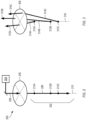
- FIG. 1 shows an example of an optical inspection system 100 for optically characterizing a sample 102, in accordance with some embodiments.
- the sample 102 is not part of the optical inspection system 100.
- the optical inspection system 100 of FIG. 1 is but one example; other suitable optical inspection systems can also be used.
- the optical inspection system 100 includes an illuminator/collector assembly 104.
- the illuminator/collector assembly 104 is a single objective lens.
- the illuminator/collector assembly 104 includes separate illumination optics and collection optics.
- the illuminator/collector assembly 104 delivers incident light 106 to the sample 102.
- the incident light 106 can have a range of propagation angles at the sample 102. In some examples, the range can have an angular width less than or equal to 20 degrees. In other examples, the range can have an angular width less than or equal to 10 degrees. In some of these examples, the incident light 106 can be collimated, with a range having an angular width of effectively zero. In examples exhibiting refraction at the sampling interface, due to differing indices of refraction, the angular width at the sampling interface can be defined in the medium having the larger range of angles.
- the incident light 106 includes more than one wavelength simultaneously, such as a plurality of discrete wavelengths or a relatively broad spectrum. In some examples, the incident light 106 includes one wavelength at a time, but the wavelength can be selectively shifted over time. In still other examples, the incident light 106 includes a relatively broad spectrum that shifts sequentially over time. In still other examples, the incident light 106 includes a plurality of relatively broad, non-overlapping spectral regions that all shift, together, over time. In some examples, the incident light 106 can be pulsed or modulated at one or more specified frequencies. In some examples, the incident light 106 can include multiple spectral regions, with each spectral regions being pulsed or modulated at its own unique frequency.
- the illuminator/collector assembly 104 can include one or more light sources, such as a single semiconductor laser, multiple semiconductor lasers having the same wavelength, multiple semiconductor lasers having different wavelengths, a single light emitting diode, multiple light emitting diodes having the same wavelength, multiple light emitting diodes having different wavelengths, one or more quantum cascade lasers, one or more superluminescent light sources, one or more amplified spontaneous emission sources, any combination of the above, or other suitable light sources.
- the illuminator/collector assembly 104 can further include one or more collimating and/or focusing optics, such as lenses, which can collimate and/or focus light produced by the one or more light sources.
- the illuminator/collector assembly 104 can further include one or more beam-steering elements, such as a beamsplitter, which can reflect an incident beam and transmit a collected beam, or can transmit an incident beam and reflect a collected beam.
- beam-steering elements such as a beamsplitter, which can reflect an incident beam and transmit a collected beam, or can transmit an incident beam and reflect a collected beam.
- the illuminator/collector assembly 104 can deliver the incident light 106 to the sample 102 through a sampling interface 108.
- the sampling interface 108 is a surface of an objective lens, the surface facing the sample 102.
- the sampling interface 108 can be an outward-facing surface of a device, which is placed into contact with the sample 102 during operation.
- the sampling interface 108 can be a cover glass, which is placed into contact with the sample 102 during operation.
- the sampling interface 108 can be a lens surface or an optical surface that is spaced apart in air or another incident medium from the sample 102.
- the sampling interface 108 can include separate first and second surfaces, where incident light passes through the first surface and return light passes through the second surface.
- the illuminator/collector assembly 104 can collect return light 110 returning from the sample 102 through the sampling interface 108 to form collected return light 112. In some examples, the incident light 106 and return light 110 pass through the same sampling interface 108.
- a sensor 114 can receive the collected return light 112. Unlike a conventional multi-pixel detector, which is largely insensitive to ray angle, the sensor 114 can measure ray intensities as a function of ray position and ray angle for the collected return light 112.
- the sensor 114 is a Shack-Hartmann sensor, which includes a microlens array 116 and a multi-pixel detector 118 at or near a focal plane of the microlens array 116.
- Another example of a suitable sensor 114 is an array of pinholes, with a multi-pixel detector disposed in an optical path after the array of pinholes. These are but two examples; other suitable sensors can also be used.
- the sensor 114 can produce a plurality of signals 120 corresponding to the measured ray intensities.
- the signals 120 are electrical.
- the signals 120 are optical, such as with optical intensities in an optical fiber.
- each pixel from the multi-pixel detector 118 can produce its own signal 120.
- one or more groups of pixels can be optically or electrically coupled together to form the signals 120.
- a computer 122 can receive the plurality of signals 120 from the sensor 114.
- the computer 122 can aggregate at least some of the received signals into a plurality of binned signals.
- Each binned signal can be formed from corresponding rays striking the sensor 114.
- Each of the corresponding rays traverses a respective optical path length within the sample 102.
- the optical path length traversed within the sample 102 by a ray of the incident light 106 is represented by the quantity A
- the optical path length traversed within the sample by a ray of the return light 110 is represented by the quantity B, so that the total optical path length traversed within the sample is represented by the quantity A+B.
- each binned signal can correspond to rays in the collected return light 112 that traverse within the sample 102 an estimated optical path length within a respective range of optical path lengths.
- the ranges of optical path length can be adjoining.
- the computer 122 can include a characterizer configured to determine a physical property 124 of the sample 102 based on the ray intensities, ray positions, and ray angles for a first subset of rays.
- the signals 120 can supply the ray intensities, ray positions, and ray angles to the computer 122.
- the characterizer can perform a first operation set using the first subset of rays and perform a second operation set using a second subset of rays in determining a physical property 124 of the sample 102.
- the subsets are determined by a ray selector (discussed below).
- the characterizer can fit the one or more of the signals to a Beer's Law calculation. In some of these examples, the characterizer can determine an absorptivity of the sample 102 based on the Beer's Law calculation. In some of these examples, the characterizer can apply different weights to the signals when determining the absorptivity of the sample 102. Beer's Law describes how much light transmits through an absorptive or scattering sample.
- T ( ⁇ ) exp(- L ⁇ c ⁇ a ( ⁇ )), where ⁇ is the wavelength of light, L is the optical path length traversed within the sample by the light, ⁇ ( ⁇ ) is a wavelength-dependent absorptivity of a substance within the sample, c is a concentration of the substance within the sample, and T ( ⁇ ) is a fraction of light exiting the sample.
- the absorptivity is the output quantity from the optical inspection system 100.
- the output quantity can be functionally equivalent to absorptivity, such as transmissivity or complex refractive index.
- the absorptivity can be an intermediate quantity, which is used internally by the optical inspection system 100 to calculate one or more other physical properties of the sample 102, such as substance concentration, or other suitable physical properties.
- the optical inspection system can include a ray selector.
- the ray selector can select the first subset of rays from the collected return light 112 at the sensor 114 that meet a first selection criterion.
- the first selection criterion can include a first range of estimated path lengths, such as path lengths traversed within the sample 102 or path length distributions, such as distributions of path length traversed within the sample 102.
- the first selection criterion can include a first range of estimated ray penetration depths within the sample 102.
- the ray selector 116 can additionally select a second subset of rays from the collected return light 112 that meet a second selection criterion.
- the first and second selection criteria can include first and second ranges of estimated path lengths or path length distributions.
- the ray selector 116 can select more than two subsets of rays, with each subset having a corresponding selection criterion. Such subsets of rays can be referred to as bins, or binned rays.
- the ray selector can operate entirely in software.
- computer 122 can include a lookup table that maps each pixel at the multi-pixel detector 118 to a corresponding optical path traversed within the sample.
- the corresponding optical path within the sample can include ray position and ray angle at the sample 102 or at a suitable longitudinal location at or near the sample 102.
- Such a lookup table can be prepared by tracing rays through the geometry of the illuminator/collector 104 assembly and through any additional elements between the sample 102 and the sensor 114. Such a ray trace can be performed once, with the results being stored in the lookup table and accessible by the computer 122.
- the computer 122 can group the detector pixels into bins, with each bin corresponding to a specified range of optical path lengths traversed within the sample 102.
- the ray selector can receive signals from corresponding pixels of the detector 118, average a first subset of the signals to form a first binned signal, average a second subset of the signals to form the second binned signal, and average additional subsets of the signals to form additional binned signals.
- the computer 122 is configured to aggregate signals from the multi-pixel detector 118 into binned signals, each binned signal corresponding to rays in the collected return light that traverse within the sample an estimated optical path length within a respective range of optical path lengths. In some of these examples, the ranges of optical path length can adjoin one another.
- the ray selector can operate at least in part in hardware.
- at least some of the binning can occur at the hardware level.
- the detector area can instead be partitioned into shapes that correspond to the bins discussed above.
- each detector area can receive rays that traverse an optical path length within the sample, within a specified range of optical path lengths.
- each detector area can produce a respective signal 120, which is directed to the computer 122.
- the ray selector can include first and second pixels of the sensor, where the first and second pixels are shaped and sized to measure ray intensities for rays within the first and second subsets of rays.
- the first and second pixels can respectively output the first and second binned signals.
- the detector can use a grid of pixels, and each pixel can produce its own signal, but the signals are combined in hardware prior to delivery at the computer 122.
- the ray selector can operate in a combination of software and hardware, with some of the binning occurring at the sensor 114 and/or at the signal level, and some of the binning occurring at the computer 122.
- the reliability of the calculations can vary from location-to-location at the detector. For some geometries, such as the geometry associated with a single scattering event (discussed below in detail), the calculation can be relatively reliable.
- the optical inspection system 100 can set a specified threshold for reliability. Signals from detector locations exceeding the threshold can be used for subsequent calculations, and signals from detector locations below the threshold can be excluded from use in the subsequent calculations.
- the optical inspection system 100 can include an optional mask 126 positioned between the microlens array 116 and the multi-pixel detector 118. The mask 126 can block rays for which the optical inspection system 100 cannot reliably determine the optical path length traversed within the sample. In some examples, the mask 126 can be directly adjacent to, in contact with, or deposited on the multi-pixel detector 118. The mask 126 can include at least one blocking portion, which blocks specified rays in the collected return light 112. The mask 126 can block particular pixels on the multi-pixel detector 124.
- the mask 126 is stationary over time.
- the mask 126 can be formed as a coating on an optical surface, where the coating includes reflective, transmissive, and/or absorptive portions that do not change over time.
- the mask 126 can be reconfigurable over time.
- the mask 126 can be formed as a reconfigurable panel, such as an array of micromirrors, which can selectively direct portions of the collected return light 112 toward the detector 118 or away from the detector 118, and can change which portions are directed toward the detector 118 or away from the detector 118 as needed.
- the thresholding can be performed in combination with the computer 122 or entirely in software by the computer 122.
- the optical inspection system 100 can assign relative weights to the binned signals.
- Each weight can represent a confidence level that the optical path lengths within the sample 102 are the same, or are within a specified range for all of the rays in the corresponding bin.
- the relative weight varies inversely with a width of an estimated distribution of the respective optical path lengths for the binned signal.
- the term inverse is intended to signify a monotonic relationship between relative weight and distribution width, without requiring a mathematically proportional relationship. For instance, as the width of an estimated distribution decreases, the relative weight can increase. As another example, as the width of an estimated distribution increases, the relative weight can decrease.
- each of the corresponding rays when traced back through the illuminator/collector assembly 104, passes a respective distance away from a corresponding incident ray within the incident light, and the relative weight varies inversely with the respective distance.
- the weight of each binned signal corresponds to a probability that light that generated the binned signal originated from a single scattering event in the sample.
- FIGS 2-7 and the accompanying discussion below address the geometry of a single scattering event.
- the computer 122 can be included in a computer system that includes hardware, firmware and software. Binning electrical signals, assigning relative weight to the binned electrical signals, determining a physical property, as well as some intermediate computational tasks, such as tracing rays and characterizing, can be executed in software, or executed in digital electronic hardware in which the ray tracing and characterizing are hard-wired into the hardware; for the purposes of this document, such hard-wired digital electronic hardware is considered to be executing ray tracing software and/or a characterizer. Examples may also be implemented as instructions stored on a computer-readable storage device, which may be read and executed by at least one processor to perform the operations described herein.
- a computer-readable storage device may include any non-transitory mechanism for storing information in a form readable by a machine (e.g., a computer).
- a computer-readable storage device may include read-only memory (ROM), random-access memory (RAM), magnetic disk storage media, optical storage media, flash-memory devices, and other storage devices and media.
- computer systems can include one or more processors, optionally connected to a network, and may be configured with instructions stored on a computer-readable storage device.
- FIGS. 2-7 address a particular geometry associated with a single scattering event in the sample. For rays satisfying this geometry, the optical path traversed within the sample can be determined with a relatively high degree of confidence. It is instructive to explore the single scattering event geometry in detail.
- FIG. 2 shows a portion of an incident optical path in an example of an optical inspection system 200, in accordance with some embodiments.
- Incident light 208 from a light source 204 optionally redirected by a mirror, strikes a central portion of a pupil of an illuminator/collector assembly 206, and propagates within sample 202 generally coincident with a central axis 210 of the illuminator/collector assembly 206.
- the incident light 208 is shown in FIG. 2 as passing through three scattering events 212A, 212B, 212C.
- each of the scattering events 212A, 212B, 212C can redirect a fraction of the incident light 208 into a respective redirected ray, with the remaining fraction continuing to propagate away from the illuminator/collector assembly 206 along the central axis 210.
- the configuration of FIG. 2 and the use of three discrete scattering events, is but one example, and that other configurations can also be used.
- the incident optical path does not necessarily have to be coincident with the optical axis.
- FIG. 3 shows a portion of a return optical path in an example of an optical inspection system, in accordance with some embodiments.
- Elements numbered 300-312 in FIG. 3 are identical in structure and function to similarly numbered elements 200-212 in FIG. 2 .
- Light rays 314A, 314B, 314C arise from respective scattering events 312A, 312B, 312C.
- the illuminator/collector 306 collects and redirects rays 314A, 314B, 314C to form return rays 316A, 316B, 316C.
- FIGS. 4A, 4B, and 4C are individual views of the three light rays in the return optical path ofFIG. 3, in accordance with some embodiments. Because rays 416A, 416B, 416C originate from points along the central axis 410 of the illuminator/collector assembly 406, rays 416A, 416B, 416C propagate within respective planes 418A, 418B, 418C, all of which include the central axis 410 of the illuminator/collector 406.
- FIG. 5 shows the rays of FIGS. 4A, 4B, and 4C , traced from the illuminator/collector assembly 506, to the array 520 of microlenses 522, to the detector 528, in accordance with some embodiments.
- the detector 528 can include a plurality of zones 530 in a one-to-one correspondence with the array 520 of microlenses 522. Each zone 530 can have a center 532 corresponding to a center 524 of a respective microlens 522.
- the array 520 of microlenses 522 redirects rays 516A, 516B, 516C to form rays 526A, 526B, 526C, which strike detector 528 at locations 534A, 534B, 534C.
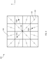
- FIG. 6 shows an end-on view of the detector 628 from FIG. 5 , in accordance with some embodiments.
- Each zone 630 can include a respective region 636 at which rays propagating from the sample to the Shack-Hartmann sensor propagate in a plane that includes the central axis of the illuminator/collector assembly.
- the regions 636 can be linear, can be radially oriented with respect to the central axis of the illuminator/collector assembly or a center 638 of the detector 628, and can include a center 632 of the respective zone 630.
- Rays 526A, 526B, 526C strike the detector 628 at respective locations 634A, 634B, 634C.
- a distance away from the zone center 632 can be proportional to (or nearly proportional to, or related with a 1:1 correspondence to) a propagation angle of rays 516A, 516B, 516C ( FIG. 5 ).
- Other possible arrangements include an input light that propagates in a direction, which is not coincident with a central axis of the optical inspection system.
- the rays can be traced back through the illuminator/collector assembly, and can intersect corresponding incident rays within the incident light.
- the incident light can have a range of propagation angles at the sampling interface, where the range can have an angular width less than or equal to 20 degrees, or preferably less than or equal to 10 degrees. As the angular range increases, it becomes more difficult to accurately determine the optical path length traversed within the sample.
- the ray paths can be used to calculate respective optical path lengths traversed within the sample.
- the ray intensities can be correlated with the optical path lengths.
- the correlation can be used to determine a physical property of the sample, such as absorptivity, transmissivity, refractive index, and others.
- the optical path lengths cannot easily be calculated.
- the propagation angle and location of a particular ray in the collected return light can determine whether or not the particular ray resides in a plane that includes the central axis (or, alternatively, the direction of the incident optical path). If the propagation angle and location of the ray show that the ray resides in one of said planes, then the contribution from the ray can be weighted relatively heavily to be used downstream to calculate the physical property of the sample. If the propagation angle and location of the ray show that the ray does not reside in one of said planes, then the contribution from the particular ray can be weighted relatively lightly to be used downstream to calculate the physical property of the sample.
- One way to determine whether a particular ray resides in a plane that includes the central axis is to trace the ray backwards, through the illuminator/collector assembly, to the sample. There will be a particular longitudinal location at which the traced ray is a minimum distance from the central axis. This minimum distance for each traced ray can be used to determine a weight, such as relative weight, which indicates how confidently one can determine the optical path length traversed in the sample by the traced ray. If the traced ray intersects the central axis, the minimum distance is zero, and the weighting factor can be its maximum value. If the traced ray comes relatively close to the central axis, the weighting factor can be relatively high. If the traced ray passes relatively far from the central axis, the weighting factor can be relatively low. In some examples, the weighting factor for a traced ray can vary inversely with a minimum distance between the traced ray and the central axis.
- the identified region or regions can correspond to one or more detector regions at which a confidence level of an estimated optical path length falls below a threshold value.
- Other suitable ways to determine the identified detector regions can also be used.
- rays in the one or more identified detector regions can be weighted more lightly than rays outside the identified detector regions, when determining the physical property of the sample.
- each detector pixel, or suitable group of detector pixels can be assigned a relative weight.
- the relative weight can represent a confidence level that the optical path lengths within the sample are the same.
- the relative weight can represent a confidence level that the optical path lengths are similar, or are nearly the same, or span a range with a width that is within a specified percentage of the mean optical path length traversed within the sample for all the rays included in the respective bin.
- the relative weight can vary inversely with a width of an estimated distribution of the respective optical path lengths within the sample.
- each ray in the collected light when traced back through an illuminator/collector assembly, passes a respective distance away from a corresponding incident ray within the incident light, and the relative weight can vary inversely with the respective distance.
- the relative weight can correspond to a probability that corresponding rays originated from a single scattering event in the sample. Other weighting schemes are also possible.
- rays in the one or more identified detector regions can be excluded entirely when determining the physical property of the sample.
- the exclusion can be performed in software, such as by a computer, such as 122 ( FIG. 1 ). In other examples, the exclusion can be performed entirely in hardware, such as with a mask, such as 126 ( FIG. 1 ).
- FIG. 7 shows an end-on view of an example of a mask 700 disposed proximate the detector of FIG. 6 in the Shack-Hartmann sensor, in accordance with some embodiments.
- Mask 700 blocks portions 1002 and transmits portions 1004 to the detector.
- the mask 700 pass only rays that, when traced backward through the illuminator/collector assembly, pass within a threshold distance of the central axis of the illuminator/collector assembly.
- One bin, corresponding to rays that fall within transmitted portion 704 is used to calculate the physical property of the sample.
- This bin can have a relative weight of 100%, or another suitable measure.
- the other bin, corresponding to rays that fall within blocked portion 702 is not used to calculate the physical property of the sample.
- This bin can have a relative weight of 0%, or another suitable measure.
- the detector can be a multi-pixel detector, with pixels arranged in a rectangular pattern, and each pixel producing a corresponding electrical signal.
- the detector can be a multi-element detector, with regions having any suitable sizes and shapes, and each region producing a corresponding electrical signal.
- the detector can be a single-element detector, producing a single electrical signal.
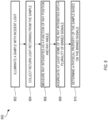
- FIG. 8 shows a flow chart of an example of a method 800 for optically characterizing a sample, in accordance with some embodiments.
- the method 800 can be executed on an optical inspection system, such as 100 ( FIG. 1 ).
- Method 800 is but one example; other suitable methods for optically inspecting a sample can also be used.
- method 800 illuminates the sample with incident light.
- method 800 collects return light returning from the sample to form collected return light.
- method 800 measures ray intensities as a function of ray position and ray angle for the collected return light.
- method 800 aggregates at least some of the electrical signals into a plurality of binned signals. The aggregation into bins can be performed purely in software, purely in hardware, or in a combination of software and hardware.
- method 800 determining a physical property of the sample based on the binned signals.
- each binned signal can correspond to rays in the collected return light that traverse within the sample an estimated optical path length within a respective range of optical path lengths.
- method 800 can further include fitting the binned signals to a Beer's Law calculation; and determining an absorptivity of the sample based on the Beer's Law calculation.
- the optical properties of a particular type of sample can vary from sample-to-sample, but often fall into a well-defined range of numerical values.
- a scattering coefficient of a particular sample typically falls within a particular range of scattering coefficients, where the range can represent a distribution of values of the scattering coefficient for a population of samples of the same type as the particular sample.
- the range can be centered around a so-called expected value, such as an expected scattering coefficient.
- the expected values can be used when designing a geometry for an optical inspection system, with the expectation that most actual measured values will be relatively close to, but different from, the expected value.
- sample-to-sample variation of a scattering and/or absorption coefficient can produce a sample-to-sample variation in the optical power reaching a detector.
- sample-to-sample variation can be undesirable, and can underutilize a full dynamic range of the detector. It is possible to design the optical inspection system to have a decreased sensitivity of detected optical power to sample-to-sample variation in scattering coefficient.
- An analytical model of the optical inspection system can assume that a light ray enters the sample at an input point, scatters a single time at a scattering location, changes direction just once at the scattering location, and exits the sample at an output point.
- an input beam is attenuated by a factor exp[-A( ⁇ s + ⁇ a )], where quantities ⁇ s , and ⁇ a are the scattering and absorption coefficients of the sample, respectively, and quantity A is an optical path length between the input point and the scattering location.
- a fraction ⁇ s of the remaining input beam is scattered towards the output, where factor ⁇ accounts for a scattering phase function.
- the light scattered toward the output location is further attenuated by an amount exp[-B( ⁇ s + ⁇ a )] before exiting the sample, where quantity B is an optical path length between the scattering location and the output point.
- a fraction of optical power exiting the sample at the output location, divided by optical power entering the sample at the input location, is given by the quantity ⁇ s exp[-L( ⁇ s + ⁇ a )], where quantity L equals quantity A+B, and is a total optical path length traversed within the sample.
- the fraction of optical power exiting the sample is relatively insensitive when its derivative equals zero, e.g., when the total optical path length traversed within the sample, L, equals an inverse of the scattering coefficient of the sample, 1/ ⁇ s .
- L 1/ ⁇ s
- the optical power reaching the detector is maximized, which is beneficial, and is relatively insensitive to sample-to-sample variations in the amount of scattering, which is also beneficial.
- the optical inspection system can be designed so that a total optical path length traversed within the sample can equal, or can be relatively close to, an inverse of an expected scattering coefficient of the sample.
- the total optical path length traversed within the sample can be within 0.1%, within 1%, within 10%, or within 50% of an inverse of an expected scattering coefficient of the sample.
- Other suitable values can also be used.
- the expected scattering coefficient can represent a distribution of values of the scattering coefficient for a population of samples of the same type as the particular sample, such as human tissue.
- the above analysis assumes a single scattering event within the sample. For geometries in which a detector element receives light that is largely due to a single high-angle scattering event, the above analysis also holds for multiple scattering events and finite positional and angular resolutions. The above analysis can also apply to confocal detection with a narrow collimated input and angularly-constrained output.
Landscapes
- Physics & Mathematics (AREA)
- Health & Medical Sciences (AREA)
- Life Sciences & Earth Sciences (AREA)
- Chemical & Material Sciences (AREA)
- Analytical Chemistry (AREA)
- Biochemistry (AREA)
- General Health & Medical Sciences (AREA)
- General Physics & Mathematics (AREA)
- Immunology (AREA)
- Pathology (AREA)
- Investigating Or Analysing Materials By Optical Means (AREA)
Applications Claiming Priority (4)
| Application Number | Priority Date | Filing Date | Title |
|---|---|---|---|
| US201462096276P | 2014-12-23 | 2014-12-23 | |
| PCT/US2015/067463 WO2016109355A1 (fr) | 2014-12-23 | 2015-12-22 | Système et procédé de vérification optique comprenant la comptabilisation des variations de la longueur du trajet optique dans un échantillon |
| EP19186560.9A EP3588061B1 (fr) | 2014-12-23 | 2015-12-22 | Système et procédé d'inspection optique comprenant la prise en compte des variations de la longueur du trajet optique dans un échantillon |
| EP15825998.6A EP3213053B1 (fr) | 2014-12-23 | 2015-12-22 | Système et méthode pour l'inspection optique tenant compte des variations de la longueur du trajet optique |
Related Parent Applications (2)
| Application Number | Title | Priority Date | Filing Date |
|---|---|---|---|
| EP19186560.9A Division EP3588061B1 (fr) | 2014-12-23 | 2015-12-22 | Système et procédé d'inspection optique comprenant la prise en compte des variations de la longueur du trajet optique dans un échantillon |
| EP15825998.6A Division EP3213053B1 (fr) | 2014-12-23 | 2015-12-22 | Système et méthode pour l'inspection optique tenant compte des variations de la longueur du trajet optique |
Publications (1)
| Publication Number | Publication Date |
|---|---|
| EP4220134A1 true EP4220134A1 (fr) | 2023-08-02 |
Family
ID=55174713
Family Applications (3)
| Application Number | Title | Priority Date | Filing Date |
|---|---|---|---|
| EP19186560.9A Active EP3588061B1 (fr) | 2014-12-23 | 2015-12-22 | Système et procédé d'inspection optique comprenant la prise en compte des variations de la longueur du trajet optique dans un échantillon |
| EP23165899.8A Pending EP4220134A1 (fr) | 2014-12-23 | 2015-12-22 | Système et procédé d'inspection optique comprenant la prise en compte de variations de longueur de trajet optique dans un échantillon |
| EP15825998.6A Active EP3213053B1 (fr) | 2014-12-23 | 2015-12-22 | Système et méthode pour l'inspection optique tenant compte des variations de la longueur du trajet optique |
Family Applications Before (1)
| Application Number | Title | Priority Date | Filing Date |
|---|---|---|---|
| EP19186560.9A Active EP3588061B1 (fr) | 2014-12-23 | 2015-12-22 | Système et procédé d'inspection optique comprenant la prise en compte des variations de la longueur du trajet optique dans un échantillon |
Family Applications After (1)
| Application Number | Title | Priority Date | Filing Date |
|---|---|---|---|
| EP15825998.6A Active EP3213053B1 (fr) | 2014-12-23 | 2015-12-22 | Système et méthode pour l'inspection optique tenant compte des variations de la longueur du trajet optique |
Country Status (6)
| Country | Link |
|---|---|
| US (4) | US10274426B2 (fr) |
| EP (3) | EP3588061B1 (fr) |
| KR (1) | KR101982950B1 (fr) |
| CN (2) | CN107209116B (fr) |
| AU (2) | AU2015374335B2 (fr) |
| WO (1) | WO2016109355A1 (fr) |
Families Citing this family (10)
| Publication number | Priority date | Publication date | Assignee | Title |
|---|---|---|---|---|
| WO2016106368A1 (fr) | 2014-12-23 | 2016-06-30 | Bribbla Dynamics Llc | Système d'inspection confocal ayant une moyenne d'éclairage et des moyennes de trajets de captage |
| EP3588061B1 (fr) | 2014-12-23 | 2023-04-19 | Apple Inc. | Système et procédé d'inspection optique comprenant la prise en compte des variations de la longueur du trajet optique dans un échantillon |
| WO2016106350A1 (fr) | 2014-12-23 | 2016-06-30 | Bribbla Dynamics Llc | Système d'inspection confocal ayant des régions d'éclairage et de collecte annulaires ne se chevauchant pas |
| WO2017040431A1 (fr) * | 2015-09-01 | 2017-03-09 | Bribbla Dynamics Llc | Architectures de commutation de référence pour la détection sans contact de substances |
| AU2017253712B8 (en) | 2016-04-21 | 2019-11-21 | Apple Inc. | Optical system for reference switching |
| WO2019067796A2 (fr) | 2017-09-29 | 2019-04-04 | Masseta Technologies Llc | Architectures d'échantillonnage optique de chemin de résolution |
| CN109842758B (zh) * | 2017-11-29 | 2022-06-07 | 超威半导体公司 | 计算传感器 |
| CN114545550B (zh) | 2018-02-13 | 2024-05-28 | 苹果公司 | 具有集成边缘外耦合器的集成光子装置 |
| US12106507B2 (en) | 2019-06-21 | 2024-10-01 | Sony Interactive Entertainment Inc. | Position detection system, image processing device, position detection method, and position detection program |
| JP7532651B2 (ja) | 2020-09-09 | 2024-08-13 | アップル インコーポレイテッド | ノイズ緩和のための光学システム |
Citations (3)
| Publication number | Priority date | Publication date | Assignee | Title |
|---|---|---|---|---|
| US20110184260A1 (en) * | 2005-02-09 | 2011-07-28 | Robinson M Ries | Methods and Apparatuses for Noninvasive Determinations of Analytes |
| JP2014163895A (ja) * | 2013-02-27 | 2014-09-08 | Canon Inc | シャック・ハルトマンセンサーを用いた状計測装置、形状計測方法 |
| US20140343383A1 (en) * | 2011-12-09 | 2014-11-20 | Sony Corporation | Measurement device, measurement method, program and recording medium |
Family Cites Families (185)
| Publication number | Priority date | Publication date | Assignee | Title |
|---|---|---|---|---|
| US3013467A (en) | 1957-11-07 | 1961-12-19 | Minsky Marvin | Microscopy apparatus |
| US3861788A (en) | 1972-08-24 | 1975-01-21 | Neotec Corp | Optical analyzer for agricultural products |
| US3805074A (en) | 1973-01-02 | 1974-04-16 | Texas Instruments Inc | Spectral scan air monitor |
| US4082464A (en) | 1976-10-07 | 1978-04-04 | Neotec Corporation | Optical analysis system having rotating filters |
| US4195311A (en) * | 1978-08-28 | 1980-03-25 | The United States Of America As Represented By The Secretary Of The Navy | Coherence length gated optical imaging system |
| DE2853458C3 (de) | 1978-09-29 | 1981-04-02 | Gebrüder Bühler AG, 9240 Uzwil | Verfahren und Vorrichtung zur Messung der relativen Helligkeit einer Probe |
| US4236076A (en) | 1979-02-26 | 1980-11-25 | Technicon Instruments Corporation | Infrared analyzer |
| US4286327A (en) | 1979-09-10 | 1981-08-25 | Trebor Industries, Inc. | Apparatus for near infrared quantitative analysis |
| US4300167A (en) * | 1980-02-07 | 1981-11-10 | Circon Corporation | Automatic iris control system |
| HU192395B (en) | 1984-02-13 | 1987-06-29 | Gabor Kemeny | Optical reflexion concentration meter |
| GB8415709D0 (en) | 1984-06-20 | 1984-07-25 | Dubilier Scient Ltd | Scanning microscope |
| US4810077A (en) | 1986-02-13 | 1989-03-07 | Spectra-Tech, Inc. | Grazing angle microscope |
| US4956796A (en) * | 1986-06-20 | 1990-09-11 | The University Of Michigan | Multiple sensor position locating system |
| US4827125A (en) | 1987-04-29 | 1989-05-02 | The United States Of America As Represented By The Secretary Of The Department Of Health And Human Services | Confocal scanning laser microscope having no moving parts |
| US4975581A (en) * | 1989-06-21 | 1990-12-04 | University Of New Mexico | Method of and apparatus for determining the similarity of a biological analyte from a model constructed from known biological fluids |
| US5065008A (en) | 1989-10-18 | 1991-11-12 | Fuji Photo Film Co., Ltd. | Scanning microscope and scanning mechanism for the same |
| US5220403A (en) | 1991-03-11 | 1993-06-15 | International Business Machines Corporation | Apparatus and a method for high numerical aperture microscopic examination of materials |
| US5483261A (en) | 1992-02-14 | 1996-01-09 | Itu Research, Inc. | Graphical input controller and method with rear screen image detection |
| US5880411A (en) | 1992-06-08 | 1999-03-09 | Synaptics, Incorporated | Object position detector with edge motion feature and gesture recognition |
| US5488204A (en) | 1992-06-08 | 1996-01-30 | Synaptics, Incorporated | Paintbrush stylus for capacitive touch sensor pad |
| US5430787A (en) * | 1992-12-03 | 1995-07-04 | The United States Of America As Represented By The Secretary Of Commerce | Compton scattering tomography |
| JP3484543B2 (ja) | 1993-03-24 | 2004-01-06 | 富士通株式会社 | 光結合部材の製造方法及び光装置 |
| US5475235A (en) * | 1993-08-09 | 1995-12-12 | Wyatt Technoloy Corporation | Control of laser light power output for use in light scattering instruments by inducing mode hopping and averaging result |
| JP3375203B2 (ja) * | 1994-08-08 | 2003-02-10 | シスメックス株式会社 | 細胞分析装置 |
| US5737084A (en) | 1995-09-29 | 1998-04-07 | Takaoka Electric Mtg. Co., Ltd. | Three-dimensional shape measuring apparatus |
| JP3422398B2 (ja) * | 1995-12-07 | 2003-06-30 | 富士通株式会社 | 重心波長モニタ方法及び装置、光増幅器並びに光通信システム |
| US5825352A (en) | 1996-01-04 | 1998-10-20 | Logitech, Inc. | Multiple fingers contact sensing method for emulating mouse buttons and mouse operations on a touch sensor pad |
| US5835079A (en) | 1996-06-13 | 1998-11-10 | International Business Machines Corporation | Virtual pointing device for touchscreens |
| US5652654A (en) | 1996-08-12 | 1997-07-29 | Asimopoulos; George | Dual beam spectrophotometer |
| JP3660761B2 (ja) * | 1996-10-03 | 2005-06-15 | 技術研究組合医療福祉機器研究所 | 散乱体の吸収情報の計測方法及び装置 |
| US5936739A (en) * | 1997-01-29 | 1999-08-10 | Sandia Corporation | Gated frequency-resolved optical imaging with an optical parametric amplifier |
| US6122042A (en) | 1997-02-07 | 2000-09-19 | Wunderman; Irwin | Devices and methods for optically identifying characteristics of material objects |
| US6198531B1 (en) * | 1997-07-11 | 2001-03-06 | University Of South Carolina | Optical computational system |
| US6310610B1 (en) | 1997-12-04 | 2001-10-30 | Nortel Networks Limited | Intelligent touch display |
| US8479122B2 (en) | 2004-07-30 | 2013-07-02 | Apple Inc. | Gestures for touch sensitive input devices |
| KR100595922B1 (ko) | 1998-01-26 | 2006-07-05 | 웨인 웨스터만 | 수동 입력 통합 방법 및 장치 |
| US7663607B2 (en) | 2004-05-06 | 2010-02-16 | Apple Inc. | Multipoint touchscreen |
| DE19811202C2 (de) | 1998-03-09 | 2002-01-17 | Gf Mestechnik Gmbh | Konfokales Scanmikroskop |
| US6248988B1 (en) | 1998-05-05 | 2001-06-19 | Kla-Tencor Corporation | Conventional and confocal multi-spot scanning optical microscope |
| US6188391B1 (en) | 1998-07-09 | 2001-02-13 | Synaptics, Inc. | Two-layer capacitive touchpad and method of making same |
| US6236459B1 (en) * | 1998-11-05 | 2001-05-22 | University Of Miami | Thin film measuring device and method |
| US6048755A (en) | 1998-11-12 | 2000-04-11 | Micron Technology, Inc. | Method for fabricating BGA package using substrate with patterned solder mask open in die attach area |
| US6999183B2 (en) * | 1998-11-18 | 2006-02-14 | Kla-Tencor Corporation | Detection system for nanometer scale topographic measurements of reflective surfaces |
| US6353226B1 (en) | 1998-11-23 | 2002-03-05 | Abbott Laboratories | Non-invasive sensor capable of determining optical parameters in a sample having multiple layers |
| JP4542637B2 (ja) | 1998-11-25 | 2010-09-15 | セイコーエプソン株式会社 | 携帯情報機器及び情報記憶媒体 |
| US6424416B1 (en) | 1999-10-25 | 2002-07-23 | Textron Systems Corporation | Integrated optics probe for spectral analysis |
| US6436613B1 (en) | 1999-08-23 | 2002-08-20 | The Arizona Board Of Regents | Integrated hybrid optoelectronic devices |
| KR100443143B1 (ko) | 2000-03-06 | 2004-08-04 | 올림푸스 가부시키가이샤 | 섹셔닝상 관찰장치에 적용되는 패턴형성부재 및 그것을이용한 섹셔닝상 관찰장치 |
| JP3707347B2 (ja) * | 2000-04-07 | 2005-10-19 | 株式会社島津製作所 | X線ct装置の画像処理方法及びx線ct装置並びにx線ct撮影用記録媒体 |
| US6587703B2 (en) | 2000-09-18 | 2003-07-01 | Photonify Technologies, Inc. | System and method for measuring absolute oxygen saturation |
| KR100806214B1 (ko) * | 2000-08-24 | 2008-02-22 | 톰슨 라이센싱 | 보정된 에러 신호 생성 방법 및 장치 |
| US6826424B1 (en) | 2000-12-19 | 2004-11-30 | Haishan Zeng | Methods and apparatus for fluorescence and reflectance imaging and spectroscopy and for contemporaneous measurements of electromagnetic radiation with multiple measuring devices |
| JP3800984B2 (ja) | 2001-05-21 | 2006-07-26 | ソニー株式会社 | ユーザ入力装置 |
| US6794658B2 (en) | 2001-06-06 | 2004-09-21 | Digital Optical Imaging Corporation | Light modulated microarray reader and methods relating thereto |
| US6519033B1 (en) * | 2001-11-19 | 2003-02-11 | Point Source Technologies, Llc | Identification of particles in fluid |
| US6594090B2 (en) | 2001-08-27 | 2003-07-15 | Eastman Kodak Company | Laser projection display system |
| JP2003173237A (ja) | 2001-09-28 | 2003-06-20 | Ricoh Co Ltd | 情報入出力システム、プログラム及び記憶媒体 |
| US20030108821A1 (en) | 2001-12-06 | 2003-06-12 | Wenhui Mei | Microlens array fabrication |
| AU2002359708A1 (en) | 2001-12-14 | 2003-07-15 | Digital Optics International Corporation | Uniform illumination system |
| US6690387B2 (en) | 2001-12-28 | 2004-02-10 | Koninklijke Philips Electronics N.V. | Touch-screen image scrolling system and method |
| US7129508B2 (en) | 2002-01-18 | 2006-10-31 | Honeywell International Inc. | Compact VCSEL sensor with multiple sensing capabilities |
| US8140147B2 (en) | 2002-04-04 | 2012-03-20 | Veralight, Inc. | Determination of a measure of a glycation end-product or disease state using a flexible probe to determine tissue fluorescence of various sites |
| GB0208100D0 (en) | 2002-04-09 | 2002-05-22 | Univ Strathclyde | Semiconductor diode laser spectrometer arrangement |
| DE10216043A1 (de) | 2002-04-11 | 2003-10-23 | Kabelschlepp Gmbh | Leitungsführungseinheit zur aktiven Führung von Leitungen, Kabeln oder dergleichen |
| US6844554B2 (en) | 2002-06-28 | 2005-01-18 | Instrumentarium Corp. | Method and arrangement for determining the concentration of a gas component in a gas mixture |
| US11275405B2 (en) | 2005-03-04 | 2022-03-15 | Apple Inc. | Multi-functional hand-held device |
| US7282723B2 (en) * | 2002-07-09 | 2007-10-16 | Medispectra, Inc. | Methods and apparatus for processing spectral data for use in tissue characterization |
| US6794671B2 (en) * | 2002-07-17 | 2004-09-21 | Particle Sizing Systems, Inc. | Sensors and methods for high-sensitivity optical particle counting and sizing |
| EP1403985A1 (fr) | 2002-09-25 | 2004-03-31 | Agilent Technologies, Inc. - a Delaware corporation - | Ensemble opto-électronique |
| US6963683B2 (en) | 2002-09-30 | 2005-11-08 | Intel Corporation | System and method for a packaging a monitor photodiode with a laser in an optical subassembly |
| US6892449B1 (en) | 2002-10-09 | 2005-05-17 | Cypress Semiconductor Corp. | Method of manufacturing electro-optical devices |
| US7170598B2 (en) | 2002-10-17 | 2007-01-30 | Direvo Biotech Ag | Multi-parameter fluorimetric analysis in a massively parallel multi-focal arrangement and the use thereof |
| US7339148B2 (en) | 2002-12-16 | 2008-03-04 | Olympus America Inc. | Confocal microscope |
| JP2004198719A (ja) | 2002-12-18 | 2004-07-15 | Tdk Corp | 光モジュール及びその製造方法 |
| WO2004057284A1 (fr) * | 2002-12-19 | 2004-07-08 | Koninklijke Philips Electronics N.V. | Systeme d'analyse optique |
| GB2399220B (en) | 2003-03-06 | 2005-07-13 | Toshiba Res Europ Ltd | Photonic quantum information system using unpolarised light |
| US7372985B2 (en) | 2003-08-15 | 2008-05-13 | Massachusetts Institute Of Technology | Systems and methods for volumetric tissue scanning microscopy |
| US6963400B1 (en) * | 2003-08-19 | 2005-11-08 | The United States Of America As Represented By The Secretary Of The Army | Systems and methods for analyzing particle systems using polarized scattered light |
| US7061623B2 (en) | 2003-08-25 | 2006-06-13 | Spectel Research Corporation | Interferometric back focal plane scatterometry with Koehler illumination |
| US20050063431A1 (en) | 2003-09-19 | 2005-03-24 | Gallup Kendra J. | Integrated optics and electronics |
| US7433042B1 (en) * | 2003-12-05 | 2008-10-07 | Surface Optics Corporation | Spatially corrected full-cubed hyperspectral imager |
| US7720291B2 (en) * | 2004-02-17 | 2010-05-18 | Corel Corporation | Iterative fisher linear discriminant analysis |
| US10620105B2 (en) | 2004-03-06 | 2020-04-14 | Michael Trainer | Methods and apparatus for determining characteristics of particles from scattered light |
| US8634072B2 (en) * | 2004-03-06 | 2014-01-21 | Michael Trainer | Methods and apparatus for determining characteristics of particles |
| JP2005257455A (ja) | 2004-03-11 | 2005-09-22 | Fuji Photo Film Co Ltd | 測定装置および測定ユニット |
| US7075046B2 (en) | 2004-07-28 | 2006-07-11 | University Of Vermont And State Agricultural College | Objective lens reference system and method |
| US8498681B2 (en) | 2004-10-05 | 2013-07-30 | Tomophase Corporation | Cross-sectional mapping of spectral absorbance features |
| EP1853874B1 (fr) | 2005-01-20 | 2009-09-02 | Zygo Corporation | Interferometre pour la determination de caracteristiques de la surface d'un objet |
| WO2006086579A2 (fr) * | 2005-02-09 | 2006-08-17 | Inlight Solutions, Inc. | Procedes et appareil de determinations non invasives d'analytes |
| CN101501464A (zh) * | 2005-02-09 | 2009-08-05 | 音莱特解决方案有限公司 | 用于分析物的无创伤性确定的方法及设备 |
| US9597024B2 (en) * | 2005-02-09 | 2017-03-21 | Medici Instruments Llc | Methods and apparatuses for noninvasive determinations of analytes |
| US20060285110A1 (en) * | 2005-02-25 | 2006-12-21 | Accent Optical Technologies, Inc. | Apparatus and method for enhanced critical dimension scatterometry |
| US20070057211A1 (en) | 2005-05-25 | 2007-03-15 | Karsten Bahlman | Multifocal imaging systems and method |
| US7203426B2 (en) | 2005-06-04 | 2007-04-10 | National Taiwan University | Optical subassembly of optical transceiver |
| CN2831098Y (zh) * | 2005-09-29 | 2006-10-25 | 公安部沈阳消防研究所 | 一种粒子计式烟雾探测装置 |
| US8537366B2 (en) * | 2005-10-11 | 2013-09-17 | Duke University | Systems and methods for endoscopic angle-resolved low coherence interferometry |
| US7440659B2 (en) | 2006-02-27 | 2008-10-21 | Wisconsin Alumni Research Foundation | Depth-resolved reflectance instrument and method for its use |
| KR100786397B1 (ko) | 2006-03-09 | 2007-12-17 | 김경철 | 레이저 빔을 이용한 면적 센서 시스템 |
| US7623233B2 (en) | 2006-03-10 | 2009-11-24 | Ometric Corporation | Optical analysis systems and methods for dynamic, high-speed detection and real-time multivariate optical computing |
| US20070258083A1 (en) | 2006-04-11 | 2007-11-08 | Optiscan Biomedical Corporation | Noise reduction for analyte detection systems |
| WO2007121593A1 (fr) | 2006-04-26 | 2007-11-01 | Abb Research Ltd | Procédé pour la mesure et la détermination de concentration dans un milieu mélangé |
| US7460248B2 (en) | 2006-05-15 | 2008-12-02 | Carestream Health, Inc. | Tissue imaging system |
| KR101265625B1 (ko) | 2006-09-11 | 2013-05-22 | 엘지전자 주식회사 | 멀티 채널을 정의하는 방송 신호를 처리하는 방송 수신기 및 그 제어방법 |
| US20090087925A1 (en) | 2007-10-01 | 2009-04-02 | Zyomyx, Inc. | Devices and methods for analysis of samples with depletion of analyte content |
| TW200823595A (en) | 2006-11-28 | 2008-06-01 | Univ Nat Taiwan | Image capture device using programmable aperture |
| US8179526B2 (en) | 2007-01-25 | 2012-05-15 | Renishaw Plc | Spectroscopic apparatus with dispersive device for collecting sample data in synchronism with relative movement of a focus |
| KR101440762B1 (ko) | 2007-02-06 | 2014-09-17 | 칼 짜이스 에스엠테 게엠베하 | 마이크로리소그래피 투영 노광 장치의 조명 시스템 내의 다수의 미러 어레이들을 감시하는 방법 및 장치 |
| DE602008006373D1 (de) | 2007-02-26 | 2011-06-01 | Koninkl Philips Electronics Nv | Verfahren und vorrichtung zur optischen gewebeanalyse |
| US8597190B2 (en) | 2007-05-18 | 2013-12-03 | Optiscan Biomedical Corporation | Monitoring systems and methods with fast initialization |
| US8098372B2 (en) * | 2007-07-23 | 2012-01-17 | Applied Materials South East Asia Pte. Ltd. | Optical inspection tool featuring multiple speed modes |
| US8089522B2 (en) * | 2007-09-07 | 2012-01-03 | Regents Of The University Of Minnesota | Spatial-temporal multi-resolution image sensor with adaptive frame rates for tracking movement in a region of interest |
| DE102007053574B4 (de) | 2007-11-09 | 2019-05-02 | Byk Gardner Gmbh | Farbmessgerät |
| CN101199413B (zh) | 2007-12-21 | 2010-04-14 | 北京高光科技有限公司 | 光学相干层析成像方法及其装置 |
| US8228601B2 (en) | 2008-05-13 | 2012-07-24 | Applied Materials Israel, Ltd. | Scanning microscopy using inhomogeneous polarization |
| JP5473265B2 (ja) | 2008-07-09 | 2014-04-16 | キヤノン株式会社 | 多層構造計測方法および多層構造計測装置 |
| WO2010073249A1 (fr) | 2008-12-24 | 2010-07-01 | Glusense, Ltd. | Détection optique implantable du glucose |
| JP4935914B2 (ja) | 2009-03-05 | 2012-05-23 | 横河電機株式会社 | 成分測定装置 |
| ATE551841T1 (de) | 2009-04-22 | 2012-04-15 | Raytrix Gmbh | Digitales bildgebungsverfahren zum synthetisieren eines bildes unter verwendung der mit einer plenoptischen kamera aufgezeichneten daten |
| JP5645445B2 (ja) | 2009-05-22 | 2014-12-24 | キヤノン株式会社 | 撮像装置及び撮像方法 |
| EP2446249B1 (fr) | 2009-06-24 | 2020-08-05 | Koninklijke Philips N.V. | Biocapteur optique avec éléments optiques de mise au point |
| WO2011011462A1 (fr) | 2009-07-20 | 2011-01-27 | Optiscan Biomedical Corporation | Connecteur réglable à espace mort réduit |
| KR101721455B1 (ko) | 2009-08-11 | 2017-04-10 | 코닌클리케 필립스 엔.브이. | 멀티-스펙트럼 이미징 |
| TWI412940B (zh) * | 2009-10-06 | 2013-10-21 | 國立交通大學 | Image reconstruction method, device and computer program for diffuse optical tomography |
| DE102009049387B4 (de) | 2009-10-14 | 2016-05-25 | Fraunhofer-Gesellschaft zur Förderung der angewandten Forschung e.V. | Vorrichtung, Bildverarbeitungsvorrichtung und Verfahren zur optischen Abbildung |
| JP4902721B2 (ja) | 2009-10-23 | 2012-03-21 | キヤノン株式会社 | 光断層画像生成装置及び光断層画像生成方法 |
| US8436296B2 (en) | 2009-11-06 | 2013-05-07 | Precision Energy Services, Inc. | Filter wheel assembly for downhole spectroscopy |
| JP4973751B2 (ja) | 2009-11-26 | 2012-07-11 | 横河電機株式会社 | 生体成分測定装置 |
| US8619237B2 (en) | 2009-12-04 | 2013-12-31 | The Trustees Of Columbia University In The City Of New York | Laser-scanning intersecting plane tomography such as for high speed volumetric optical imaging |
| KR101112144B1 (ko) | 2009-12-30 | 2012-02-14 | 부산대학교 산학협력단 | 부분 반사를 이용한 간섭 시스템 및 측정 시스템 |
| US8518643B2 (en) * | 2010-02-04 | 2013-08-27 | Pacific Biosciences Of California, Inc. | Method to improve single molecule analyses |
| US7884933B1 (en) | 2010-05-05 | 2011-02-08 | Revolutionary Business Concepts, Inc. | Apparatus and method for determining analyte concentrations |
| US8951472B2 (en) | 2010-07-19 | 2015-02-10 | Andalyze, Inc. | Portable fluorimetric apparatus, method and system |
| TWI418774B (zh) | 2010-08-06 | 2013-12-11 | 大區域光學檢測裝置及其運作方法 | |
| US10292589B2 (en) | 2010-09-20 | 2019-05-21 | California Institute Of Technology | Acoustic-assisted iterative wave form optimization for deep tissue focusing |
| JP5621973B2 (ja) * | 2010-09-30 | 2014-11-12 | 国立大学法人名古屋大学 | ナノ構造体を利用した検出方法及び検出システム |
| US8866107B2 (en) | 2011-01-19 | 2014-10-21 | Howard Hughes Medical Institute | Wavefront compensation for deep tissue optical microscopy |
| GB201107556D0 (en) | 2011-05-06 | 2011-06-22 | Sheblee Jafer | Spatial resolution enhancements in multibeam confocal scanning systems |
| CN103748441B (zh) | 2011-06-07 | 2016-12-28 | 精量电子(美国)有限公司 | 用于流体传感的光学传感装置和光学传感方法 |
| EP2729784A4 (fr) | 2011-07-06 | 2015-05-13 | Optiscan Biomedical Corp | Cellule échantillon pour système d'analyse de fluide |
| FR2978255B1 (fr) | 2011-07-22 | 2014-02-21 | Horiba Jobin Yvon Sas | Dispositif optique d'eclairage conoscopique a cone creux pour microscope optique et procede de microscopie optique en conoscopie |
| JP5882674B2 (ja) | 2011-10-24 | 2016-03-09 | キヤノン株式会社 | 多波長干渉計、計測装置および計測方法 |
| EP2783193A4 (fr) | 2011-11-03 | 2015-08-26 | Verifood Ltd | Système de spectrométrie à faible coût pour analyse d'aliments d'utilisateur final |
| EP2600637A1 (fr) * | 2011-12-02 | 2013-06-05 | Fraunhofer-Gesellschaft zur Förderung der angewandten Forschung e.V. | Appareil et procédé pour le positionnement de microphone en fonction de la densité spatiale de puissance |
| CN102519976A (zh) | 2011-12-26 | 2012-06-27 | 上海大学 | 光学元件亚表面缺陷数字全息检测装置 |
| EP2629050B2 (fr) | 2012-02-16 | 2017-02-15 | Sick AG | Capteur de triangulation |
| US9024252B2 (en) | 2012-02-21 | 2015-05-05 | Entegris-Jetalon Solutions, Inc. | Optical sensor apparatus to detect light based on the refractive index of a sample |
| JP6393679B2 (ja) | 2012-04-30 | 2018-09-19 | メイヨ フォンデーシヨン フォー メディカル エジュケーション アンド リサーチ | 時間および空間変動測定値のフォーカス位置特定を改善するための分光システムおよび方法 |
| US9075015B2 (en) * | 2012-06-04 | 2015-07-07 | Frederick W. Shapiro | Universal tool for automated gem and mineral identification and measurement |
| JP2014016235A (ja) * | 2012-07-09 | 2014-01-30 | Seiko Epson Corp | 光吸収係数分布推定装置、濃度測定装置及び光吸収係数分布推定装置の制御方法 |
| US9585604B2 (en) | 2012-07-16 | 2017-03-07 | Zyomed Corp. | Multiplexed pathlength resolved noninvasive analyzer apparatus with dynamic optical paths and method of use thereof |
| US9766126B2 (en) | 2013-07-12 | 2017-09-19 | Zyomed Corp. | Dynamic radially controlled light input to a noninvasive analyzer apparatus and method of use thereof |
| JP6212312B2 (ja) * | 2012-08-13 | 2017-10-11 | パナソニック株式会社 | 物体内部推定装置およびその方法 |
| JP2014075780A (ja) * | 2012-09-14 | 2014-04-24 | Ricoh Co Ltd | 撮像装置及び撮像システム |
| JP2014095688A (ja) * | 2012-10-09 | 2014-05-22 | Ricoh Co Ltd | 撮像装置及び撮像システム |
| JP6091176B2 (ja) * | 2012-11-19 | 2017-03-08 | キヤノン株式会社 | 画像処理方法、画像処理プログラム、画像処理装置および撮像装置 |
| CN103842797B (zh) | 2013-05-10 | 2015-10-21 | 浙江大学 | 一维全场彩虹测量装置及测量方法 |
| JP6270214B2 (ja) * | 2013-11-25 | 2018-01-31 | 株式会社リガク | X線分析装置の光軸調整方法及びx線分析装置 |
| JP2015119067A (ja) | 2013-12-19 | 2015-06-25 | ソニー株式会社 | 固体撮像装置、光検出器、および電子機器 |
| EP3090239A4 (fr) | 2014-01-03 | 2018-01-10 | Verifood Ltd. | Systèmes de spectrométrie, procédés, et applications associées |
| US9647419B2 (en) | 2014-04-16 | 2017-05-09 | Apple Inc. | Active silicon optical bench |
| US9494535B2 (en) * | 2014-04-21 | 2016-11-15 | Kla-Tencor Corporation | Scatterometry-based imaging and critical dimension metrology |
| WO2016054079A1 (fr) | 2014-09-29 | 2016-04-07 | Zyomed Corp. | Systèmes et procédés pour la détection et la mesure du glucose sanguin du sang et d'autres analytes à l'aide du calcul de collision |
| US9804027B2 (en) | 2014-09-29 | 2017-10-31 | Aurrion, Inc. | Heterogeneous spectroscopic transceiving photonic integrated circuit sensor |
| WO2016106368A1 (fr) | 2014-12-23 | 2016-06-30 | Bribbla Dynamics Llc | Système d'inspection confocal ayant une moyenne d'éclairage et des moyennes de trajets de captage |
| EP3588061B1 (fr) | 2014-12-23 | 2023-04-19 | Apple Inc. | Système et procédé d'inspection optique comprenant la prise en compte des variations de la longueur du trajet optique dans un échantillon |
| WO2016106350A1 (fr) | 2014-12-23 | 2016-06-30 | Bribbla Dynamics Llc | Système d'inspection confocal ayant des régions d'éclairage et de collecte annulaires ne se chevauchant pas |
| US9395293B1 (en) | 2015-01-12 | 2016-07-19 | Verily Life Sciences Llc | High-throughput hyperspectral imaging with superior resolution and optical sectioning |
| CN104614084A (zh) | 2015-01-20 | 2015-05-13 | 顾樵 | 一种光子探测装置及其使用方法 |
| EP3286587A4 (fr) | 2015-04-20 | 2018-12-26 | Skorpios Technologies, Inc. | Coupleurs à sortie verticale pour des dispositifs photoniques |
| JP2017017537A (ja) | 2015-07-01 | 2017-01-19 | キヤノン株式会社 | 電子機器及び表示制御方法 |
| CN105067489B (zh) * | 2015-08-07 | 2018-01-09 | 中国科学院计算技术研究所 | 一种基于动态光散射技术的悬浮颗粒粒径测量装置及方法 |
| WO2017040431A1 (fr) | 2015-09-01 | 2017-03-09 | Bribbla Dynamics Llc | Architectures de commutation de référence pour la détection sans contact de substances |
| CN105223163A (zh) | 2015-09-30 | 2016-01-06 | 上海理工大学 | 一种基于古依相移π反转检测物体精细结构的装置 |
| CN105438912B (zh) | 2016-01-28 | 2018-07-13 | 中国人民解放军信息工程大学 | 一种位置监控方法及系统 |
| WO2017139649A2 (fr) | 2016-02-12 | 2017-08-17 | Massachusetts Institute Of Technology | Procédé et appareil d'imagerie d'échantillons de tissu non sectionnés |
| WO2017151416A2 (fr) | 2016-03-02 | 2017-09-08 | Corning Optical Communications LLC | Ensembles et agencements d'interposeur permettant de coupler au moins une fibre optique à au moins un dispositif optoélectronique |
| CN113899452B (zh) | 2016-04-21 | 2024-04-19 | 苹果公司 | 用于参考切换的多路复用和编码 |
| AU2017253712B8 (en) | 2016-04-21 | 2019-11-21 | Apple Inc. | Optical system for reference switching |
| WO2019067796A2 (fr) | 2017-09-29 | 2019-04-04 | Masseta Technologies Llc | Architectures d'échantillonnage optique de chemin de résolution |
| CN114545550B (zh) | 2018-02-13 | 2024-05-28 | 苹果公司 | 具有集成边缘外耦合器的集成光子装置 |
| US11206985B2 (en) * | 2018-04-13 | 2021-12-28 | Hi Llc | Non-invasive optical detection systems and methods in highly scattering medium |
| US11378808B2 (en) | 2018-07-18 | 2022-07-05 | Idex Health & Science Llc | Laser systems and optical devices for laser beam shaping |
| DE112019004770T5 (de) * | 2018-09-24 | 2021-08-12 | Ams Sensors Asia Pte. Ltd. | Verbesserte Beleuchtungseinrichtung |
| JP7532651B2 (ja) | 2020-09-09 | 2024-08-13 | アップル インコーポレイテッド | ノイズ緩和のための光学システム |
| KR20220046168A (ko) * | 2020-10-07 | 2022-04-14 | 삼성전자주식회사 | 분석 물질의 농도 추정 장치 및 방법과, 신호 측정 장치 |
-
2015
- 2015-12-22 EP EP19186560.9A patent/EP3588061B1/fr active Active
- 2015-12-22 EP EP23165899.8A patent/EP4220134A1/fr active Pending
- 2015-12-22 CN CN201580065101.XA patent/CN107209116B/zh active Active
- 2015-12-22 EP EP15825998.6A patent/EP3213053B1/fr active Active
- 2015-12-22 AU AU2015374335A patent/AU2015374335B2/en active Active
- 2015-12-22 WO PCT/US2015/067463 patent/WO2016109355A1/fr not_active Ceased
- 2015-12-22 KR KR1020177014847A patent/KR101982950B1/ko active Active
- 2015-12-22 CN CN202010795936.3A patent/CN111929280B/zh active Active
-
2017
- 2017-09-27 US US15/717,651 patent/US10274426B2/en active Active
-
2018
- 2018-06-20 AU AU2018204450A patent/AU2018204450B2/en active Active
-
2019
- 2019-03-07 US US16/296,010 patent/US11035793B2/en active Active
-
2021
- 2021-06-14 US US17/346,390 patent/US11726036B2/en active Active
-
2023
- 2023-06-04 US US18/205,551 patent/US20230314321A1/en active Pending
Patent Citations (3)
| Publication number | Priority date | Publication date | Assignee | Title |
|---|---|---|---|---|
| US20110184260A1 (en) * | 2005-02-09 | 2011-07-28 | Robinson M Ries | Methods and Apparatuses for Noninvasive Determinations of Analytes |
| US20140343383A1 (en) * | 2011-12-09 | 2014-11-20 | Sony Corporation | Measurement device, measurement method, program and recording medium |
| JP2014163895A (ja) * | 2013-02-27 | 2014-09-08 | Canon Inc | シャック・ハルトマンセンサーを用いた状計測装置、形状計測方法 |
Non-Patent Citations (1)
| Title |
|---|
| HUI XIA ET AL: "Study of optical parameters of polystyrene spheres in dense aqueous suspensions", APPLIED OPTICS, OPTICAL SOCIETY OF AMERICA, WASHINGTON, DC; US, vol. 51, no. 16, 23 May 2012 (2012-05-23), pages 3263 - 3268, XP001575951, ISSN: 0003-6935, [retrieved on 20120523], DOI: 10.1364/AO.51.003263 * |
Also Published As
| Publication number | Publication date |
|---|---|
| EP3213053A1 (fr) | 2017-09-06 |
| US20230314321A1 (en) | 2023-10-05 |
| AU2018204450A1 (en) | 2018-07-12 |
| WO2016109355A1 (fr) | 2016-07-07 |
| EP3588061B1 (fr) | 2023-04-19 |
| AU2015374335B2 (en) | 2018-03-29 |
| CN111929280B (zh) | 2025-03-04 |
| EP3213053B1 (fr) | 2019-08-28 |
| US20180017491A1 (en) | 2018-01-18 |
| US11035793B2 (en) | 2021-06-15 |
| CN111929280A (zh) | 2020-11-13 |
| AU2018204450B2 (en) | 2019-07-18 |
| US10274426B2 (en) | 2019-04-30 |
| US20190204221A1 (en) | 2019-07-04 |
| EP3588061A1 (fr) | 2020-01-01 |
| US11726036B2 (en) | 2023-08-15 |
| AU2015374335A1 (en) | 2017-07-06 |
| CN107209116B (zh) | 2020-08-07 |
| CN107209116A (zh) | 2017-09-26 |
| KR20170080646A (ko) | 2017-07-10 |
| US20210302313A1 (en) | 2021-09-30 |
| KR101982950B1 (ko) | 2019-05-27 |
Similar Documents
| Publication | Publication Date | Title |
|---|---|---|
| US11726036B2 (en) | Optical inspection system and method including accounting for variations of optical path length within a sample | |
| US10551605B2 (en) | Confocal inspection system having non-overlapping annular illumination and collection regions | |
| CN107430263B (zh) | 具有平均照明路径和平均收集路径的共焦检查系统 | |
| US20190234862A1 (en) | Analysis device for determining particulate matter | |
| US10018550B2 (en) | System and method for analyzing blood cell | |
| RU2670809C9 (ru) | Устройство измерения шероховатости поверхности | |
| CN103149158A (zh) | 一种双棱镜水质监测光纤传感系统 | |
| NL8301089A (nl) | Werkwijze voor het inspecteren van transparante staven. | |
| JP6542906B2 (ja) | 少なくとも部分的に透明な物体の表面に関連する表面データおよび/または測定データを決定するための方法および装置 | |
| JP7223752B2 (ja) | 粒子径分布測定装置及び粒子径分布測定装置用プログラム | |
| CN110836642A (zh) | 一种基于三角测量法的彩色三角位移传感器及其测量方法 | |
| CN104792732A (zh) | 一种光源分布自参照的折光计 | |
| US9952150B2 (en) | Device for measuring the scattering of a sample | |
| US11709124B2 (en) | Particle sensor sample area qualification without a physical slit | |
| EP3662264A1 (fr) | Procédé et appareil pour l'analyse bactérienne | |
| CN115307736B (zh) | 一种分光色度计集光系统 | |
| JPH03214038A (ja) | 空気中に散布されたエアロゾルと粉麈などの測定装置 | |
| CN115752716A (zh) | 一种基于光栅的高灵敏度光信号探测光机结构 | |
| RU104303U1 (ru) | Устройство для лазерной триангуляции | |
| RU2694285C2 (ru) | Устройство для измерения распределения показателя преломления градиентных оптических заготовок |
Legal Events
| Date | Code | Title | Description |
|---|---|---|---|
| PUAI | Public reference made under article 153(3) epc to a published international application that has entered the european phase |
Free format text: ORIGINAL CODE: 0009012 |
|
| STAA | Information on the status of an ep patent application or granted ep patent |
Free format text: STATUS: REQUEST FOR EXAMINATION WAS MADE |
|
| 17P | Request for examination filed |
Effective date: 20230331 |
|
| AC | Divisional application: reference to earlier application |
Ref document number: 3213053 Country of ref document: EP Kind code of ref document: P Ref document number: 3588061 Country of ref document: EP Kind code of ref document: P |
|
| AK | Designated contracting states |
Kind code of ref document: A1 Designated state(s): AL AT BE BG CH CY CZ DE DK EE ES FI FR GB GR HR HU IE IS IT LI LT LU LV MC MK MT NL NO PL PT RO RS SE SI SK SM TR |
|
| STAA | Information on the status of an ep patent application or granted ep patent |
Free format text: STATUS: EXAMINATION IS IN PROGRESS |
|
| 17Q | First examination report despatched |
Effective date: 20250226 |