EP4220227A1 - Puce de télémétrie cohérente en réseau et son système - Google Patents
Puce de télémétrie cohérente en réseau et son système Download PDFInfo
- Publication number
- EP4220227A1 EP4220227A1 EP20954949.2A EP20954949A EP4220227A1 EP 4220227 A1 EP4220227 A1 EP 4220227A1 EP 20954949 A EP20954949 A EP 20954949A EP 4220227 A1 EP4220227 A1 EP 4220227A1
- Authority
- EP
- European Patent Office
- Prior art keywords
- light
- signal
- chip
- ranging
- array
- Prior art date
- Legal status (The legal status is an assumption and is not a legal conclusion. Google has not performed a legal analysis and makes no representation as to the accuracy of the status listed.)
- Pending
Links
Images


Classifications
-
- G—PHYSICS
- G01—MEASURING; TESTING
- G01S—RADIO DIRECTION-FINDING; RADIO NAVIGATION; DETERMINING DISTANCE OR VELOCITY BY USE OF RADIO WAVES; LOCATING OR PRESENCE-DETECTING BY USE OF THE REFLECTION OR RERADIATION OF RADIO WAVES; ANALOGOUS ARRANGEMENTS USING OTHER WAVES
- G01S7/00—Details of systems according to groups G01S13/00, G01S15/00, G01S17/00
- G01S7/48—Details of systems according to groups G01S13/00, G01S15/00, G01S17/00 of systems according to group G01S17/00
- G01S7/481—Constructional features, e.g. arrangements of optical elements
- G01S7/4817—Constructional features, e.g. arrangements of optical elements relating to scanning
-
- G—PHYSICS
- G01—MEASURING; TESTING
- G01S—RADIO DIRECTION-FINDING; RADIO NAVIGATION; DETERMINING DISTANCE OR VELOCITY BY USE OF RADIO WAVES; LOCATING OR PRESENCE-DETECTING BY USE OF THE REFLECTION OR RERADIATION OF RADIO WAVES; ANALOGOUS ARRANGEMENTS USING OTHER WAVES
- G01S17/00—Systems using the reflection or reradiation of electromagnetic waves other than radio waves, e.g. lidar systems
- G01S17/02—Systems using the reflection of electromagnetic waves other than radio waves
- G01S17/06—Systems determining position data of a target
- G01S17/08—Systems determining position data of a target for measuring distance only
- G01S17/32—Systems determining position data of a target for measuring distance only using transmission of continuous waves, whether amplitude-, frequency-, or phase-modulated, or unmodulated
- G01S17/36—Systems determining position data of a target for measuring distance only using transmission of continuous waves, whether amplitude-, frequency-, or phase-modulated, or unmodulated with phase comparison between the received signal and the contemporaneously transmitted signal
-
- G—PHYSICS
- G01—MEASURING; TESTING
- G01S—RADIO DIRECTION-FINDING; RADIO NAVIGATION; DETERMINING DISTANCE OR VELOCITY BY USE OF RADIO WAVES; LOCATING OR PRESENCE-DETECTING BY USE OF THE REFLECTION OR RERADIATION OF RADIO WAVES; ANALOGOUS ARRANGEMENTS USING OTHER WAVES
- G01S7/00—Details of systems according to groups G01S13/00, G01S15/00, G01S17/00
- G01S7/48—Details of systems according to groups G01S13/00, G01S15/00, G01S17/00 of systems according to group G01S17/00
- G01S7/491—Details of non-pulse systems
- G01S7/4911—Transmitters
-
- G—PHYSICS
- G01—MEASURING; TESTING
- G01S—RADIO DIRECTION-FINDING; RADIO NAVIGATION; DETERMINING DISTANCE OR VELOCITY BY USE OF RADIO WAVES; LOCATING OR PRESENCE-DETECTING BY USE OF THE REFLECTION OR RERADIATION OF RADIO WAVES; ANALOGOUS ARRANGEMENTS USING OTHER WAVES
- G01S7/00—Details of systems according to groups G01S13/00, G01S15/00, G01S17/00
- G01S7/48—Details of systems according to groups G01S13/00, G01S15/00, G01S17/00 of systems according to group G01S17/00
- G01S7/491—Details of non-pulse systems
- G01S7/4912—Receivers
- G01S7/4913—Circuits for detection, sampling, integration or read-out
- G01S7/4914—Circuits for detection, sampling, integration or read-out of detector arrays, e.g. charge-transfer gates
-
- G—PHYSICS
- G01—MEASURING; TESTING
- G01S—RADIO DIRECTION-FINDING; RADIO NAVIGATION; DETERMINING DISTANCE OR VELOCITY BY USE OF RADIO WAVES; LOCATING OR PRESENCE-DETECTING BY USE OF THE REFLECTION OR RERADIATION OF RADIO WAVES; ANALOGOUS ARRANGEMENTS USING OTHER WAVES
- G01S7/00—Details of systems according to groups G01S13/00, G01S15/00, G01S17/00
- G01S7/48—Details of systems according to groups G01S13/00, G01S15/00, G01S17/00 of systems according to group G01S17/00
- G01S7/491—Details of non-pulse systems
- G01S7/4912—Receivers
- G01S7/4917—Receivers superposing optical signals in a photodetector, e.g. optical heterodyne detection
Definitions
- the present application relates to the technical field of the LiDAR, and specifically relates to an array coherent ranging chip and a system thereof.
- LiDAR Laser detection and ranging
- LiDAR Laser detection and ranging
- a remote sensing technology that has a broad and irreplaceable application in the fields of automatic pilot, virtual/augmented reality, optical communication, etc., which completes the detection on the distance from a to-be-measured object by irradiating a laser beam of a specific wavelength and direction onto the to-be-measured object, and measuring the returned signal.
- the first one is the time-of-flight method, which determines the distance from an object by detecting the time delay between the emitted and received optical pulses.
- the disadvantages of this method are that the ranging distance is relatively short, and this method can only implement single-point measurement, and is of a very low interference resistance.
- the second one is coherent detection, and according to the different laser modulation methods, there are several relatively common solutions such as the frequency modulated continuous wave (FMCW) and the chirped amplitude modulation (CAM).
- FMCW frequency modulated continuous wave
- CAM chirped amplitude modulation
- flashes implement emissions at and receptions from multiple angles within field-of-view at the same time by means of a wide-emission-angle light source and a sensor array, so as to obtain the distance information on the basis of the time-of-flight method (TOF).
- TOF time-of-flight method
- the total power of the light source output is limited by the safety power limit for human eyes, and because of the simultaneous emitting from the light source at multiple angles, the emitting power within a unit angle is limited, and since the intensity of optical signal reflected by an object has an inverse-square relationship with the distance from the object, whereas the time-of-flight sensor array can only identify signals above the noise threshold, the ranging distance is limited.
- the ambient light contains a component having the emission wavelength
- environmental interference and superposition of signals may lead to saturation of the sensors and make the sensors unable to identify the target signal.
- the solution of flashes that is based on the time-of-flight method is very susceptible to the environmental light.
- embodiments of the present application provide an array coherent ranging chip and a system thereof to solve the technical problem that ranging by the LiDAR is limited and the interference resistance is poor in the related art.
- an array coherent ranging chip which includes a modulated light source unit, an on-chip emission unit and a reception array.
- the modulated light source unit is used for generating a modulated light beam and splitting the modulated light beam into signal light and reference light, and then outputting the signal light and the reference light.
- the on-chip emission unit is used for irradiating the signal light onto a target object at a preset divergence angle so as to have the signal light reflected to form multi-angle signal light.
- the reception array is used for receiving the reference light and the multi-angle signal light and respectively performing conversion and detection on both the reference light and the signal light of each angle so as to obtain a plurality of ranging signals.
- the reception array may include a plurality of reception units, and each of the reception units includes a diffraction structure, a light combination assembly and a sensor.
- the diffraction structure may be configured to receive reflected light of a corresponding angle and guides the reflected light of the corresponding angle to an input end of the light combination assembly.
- the light combination assembly may be configured to receive the reference light and the reflected light of the corresponding angle, combine the reference light and the reflected light of the corresponding angle into a composite signal, and divide the composite signal into a first detection signal and a second detection signal.
- the sensor may be configured to receive the first detection signal and the second detection signal, convert the first detection signal and the second detection signal into electric signals, and output a difference between the electric signals to obtain the ranging signals.
- the reception array may further include a first beam splitting region.
- the first beam splitting region may include a plurality of beam splitting units.
- the first beam splitting region may receive the reference light and perform a beam splitting thereon, and then respectively transmit the split beams from the reference light into the light combination assembly of each of the reception units.
- an operating wavelength range of the modulated light source unit may include a visible band and a near-infrared band.
- the diffraction structure may include a one-dimensional or two-dimensional diffractive optical element.
- the light combination assembly may include any one of a diffractive optical element, a diffraction grating, a metasurface, a Y-branch, a multimode interference coupler, a directional coupler, a star coupler and a polarizing beamsplitter.
- the sensor may include any one of an avalanche photodiode, a photomultiplier tube and a PIN diode.
- the modulated light source unit may include a modulation unit and a beam splitting unit.
- the modulation unit may include a light source and a signal generator.
- the light source may have a modulation manner which is external modulation or internal modulation.
- the modulation unit includes an intensity modulator, whereas when that is based on a principle of internal modulation, the modulation unit does not include an intensity modulator.
- the beam splitting unit may include any one of a Y-branch, a star coupler, a multimode interference coupler, a directional coupler, a polarizing beamsplitter, a partially diffractive and partially transmissive waveguide grating.
- the on-chip emission unit may include an on-chip beam expansion structure and a diffraction structure.
- the on-chip beam expansion structure may be configured to shape and then output the signal light.
- the diffraction structure may be configured to irradiate the signal light, after being shaped, onto a target object at the preset divergence angle so as to have the signal light reflected to form multi-angle signal light.
- the on-chip beam expansion structure may include any one of a thermal insulation inversely tapered waveguide, a planar waveguide concave reflection mirror, a planar waveguide lens based on a waveguide layer with a thickness that gradually changes, a micro-nano-structure based planar waveguide lens with a refractive index that gradually changes, a cascaded beam splitter and a star coupler.
- the diffraction structure may include a waveguide diffraction grating array or a planar waveguide grating.
- the on-chip emission unit may include an optical phased array.
- the optical phased array may include a second beam splitting region, a phased region and an output unit.
- the second beam splitting region may be used for performing a beam splitting on the signal light and output the split beams from the signal light into the phased region.
- the phased region may be used for performing phase modulation on the split beams from the signal light.
- the output unit may be used for outputting the signal light with a modulated phase so as to irradiate signal lights of two dimensions onto the target object.
- the on-chip emission unit may perform scans, under the control of an exterior scanning device, by means of the signal light in various directions of emission.
- on-chip optical elements and on-chip electrical elements may be integrated on one chip or respectively on two chips.
- the two chips may be interconnected via an optical signal or an electrical signal.
- the array coherent ranging chip may further include any one of a rectangular waveguide, a ridge waveguide and a slot waveguide which are used for transmitting an on-chip optical signal, wherein when the operating wavelength is within the visible band, a platform that is hybrid-integrated on the basis of silicon nitride and silicon may be employed for chip integration, and wherein silicon nitride may be employed as waveguide material, and when the operating wavelength is within the near-infrared band, chip integration may be performed on the basis of a silicon platform disposed on an insulator.
- an array coherent ranging system which includes a signal processing unit and the array coherent ranging chip according to the first aspect of embodiments of the present application.
- the signal processing unit is configured to receive the ranging signals output by the array coherent ranging chip and calculate a distance from the target object by a spectrum analysis.
- the array coherent ranging chip provided by embodiments of the present application implements the laser ranging by employing the form of a chip, whereof the structure is compact, the reliability is high, and the cost in ranging is reduced.
- generated ranging signal is in direct proportion to the product of amplitudes of the reference light and the signal light, and therefore the choice of a proper reference power can implement the control on signal amplitude, thereby the range of ranging is able to be extended, and besides, a component with a wavelength different from the light source is not able to form stable interference signal, thereby providing the effect of ambient light interference resistance.
- receiving multi-angle reflected lights by means of a reception array enables parallel processing of data on multiple pixels, thereby the number of points collected per unit time can be greatly increased in comparison with scanning coherent LiDARs/radars.
- Array coherent ranging systems provided by embodiments of the present application can perform a ranging of the distance from a target object, whereof the structure is simple and the cost is low, and can enable miniaturization and SoPC (System on a Programmable Chip), whereby the integration can be facilitated.
- the ranging systems employ the way of coherent detection, thereby enabling signal amplification, besides, a component with a wavelength different from the light source is not able to form stable interference signal, thereby providing the effect of ambient light interference resistance.
- orientations or positional relationships indicated by the terms “center”, “upper”, “lower”, “left”, “right”, “vertical”, “horizontal”, “inside”, “outside” and the like are based on orientations or positional relationships shown in the drawings, and are merely to facilitate and simplify the description, rather than indicating or implying devices or elements that are referred to must have a particular orientation, or must be constructed or operated in a particular orientation, and thus, these terms cannot be understood as limitations to the present application.
- the terms “first”, “second” and “third” are used for descriptive purposes only, and are not to be understood as indicating or implying the relative importance.
- the terms “installed”, “connected”, “coupled” should be broadly understood, for instance, it may be a fixed connection, a detachable connection or an integral connection, may be a mechanical connection or an electrical connection, may be a direct connection or an indirect connection via an intermediate medium, or otherwise may be an interior communication between two elements, and may be a wireless connection or a wired connection.
- installed may be a fixed connection, a detachable connection or an integral connection, may be a mechanical connection or an electrical connection, may be a direct connection or an indirect connection via an intermediate medium, or otherwise may be an interior communication between two elements, and may be a wireless connection or a wired connection.
- an array coherent ranging chip as shown in FIG. 1 , which includes a modulated light source unit 101, an on-chip emission unit 102 and a reception array 103.
- the modulated light source unit 101 is used for generating a modulated light beam and splitting the modulated light beam into signal light and reference light, and then outputting the signal light and the reference light.
- the on-chip emission unit 102 is used for irradiating the signal light onto a target object at a preset divergence angle so as to have the signal light reflected to form multi-angle signal light.
- the reception array 103 is used for receiving the reference light and the multi-angle signal light and respectively performing conversion and detection on both the reference light and the signal light of each angle so as to obtain a plurality of ranging signals.
- An array coherent ranging chip provided by this embodiment of the present application implements the laser ranging by employing the form of a chip, whereof the structure is compact, the reliability is high, and the cost in ranging is reduced.
- generated ranging signal is in direct proportion to the product of amplitudes of the reference light and the signal light, and therefore the choice of a proper reference power can implement the control on signal amplitude, thereby the range of ranging is able to be extended, and besides, a component with a wavelength different from the light source is not able to form stable interference signal, thereby providing the effect of ambient light interference resistance.
- receiving multi-angle reflected lights by means of a reception array enables parallel processing of data on multiple pixels, thereby the number of points collected per unit time can be greatly increased in comparison with scanning coherent LiDARs/radars.
- the reception array 103 includes a plurality of reception units.
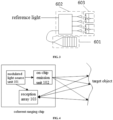
- Each of the reception units includes a diffraction structure 601, a light combination assembly 602 and a sensor 603.
- the diffraction structure 601 is configured to receive reflected light of a corresponding angle and guides the reflected light of the corresponding angle to an input end of the light combination assembly 602.
- the light combination assembly 602 is configured to receive the reference light and the reflected light of the corresponding angle, combine the reference light and the reflected light of the corresponding angle into a composite signal, and divide the composite signal into a first detection signal and a second detection signal.
- the sensor 603 is configured to receive the first detection signal and the second detection signal, convert the first detection signal and the second detection signal into electric signals, and output a difference between the electric signals to obtain the ranging signals.
- the light combination assembly 602 may convert the incident reference light E Lo and the reflected light E S e i ⁇ of the corresponding angle to form four mixed signals with amplitudes respectively of 2 E S ⁇ E LO / 2 , 2 E S + E LO / 2 , 2 E S + iE LO / 2 and 2 E S ⁇ iE LO / 2 as output, wherein the first two and the last two of the four mixed signals may each form a group of signals respectively with phase differences of 0 degree and 180 degrees.
- the four signals output by the light combination assembly 602 may be received by the sensor of the reception unit, wherein the two groups of signals respectively with phase differences of 0 degree and 180 degrees may each form a balanced detection by a signal circuit of the sensor 603.
- the first detection signal and the second detection signal may each contain two sub-signals, and the two sub-signals of each detection signal may be respectively input into two input ports of the balanced detector.
- the sensor may convert the incident light signals into electric signals. After an acquisition of the difference values being performed on the two groups of signals, the high frequency component and the direct-current component may be filtered, then the two groups of signals may be amplified and output, and then the difference values of signals respectively from the two groups of signals may be squared and summed so as to obtain an output signal, thereby the impact of phase on signals can be removed by filtering.
- the implementation of the light combination assembly 602 may include but not limited to a diffractive optical element, a diffraction grating, a metasurface, a Y-branch, a multimode interference coupler, a directional coupler, a star coupler and a polarizing beamsplitter.
- the diffraction structure 601 may include a one-dimensional or two-dimensional diffractive optical element, such as a waveguide diffraction grating array or a planar waveguide grating.
- the sensor 603 may be composed of four detection arrays which are in one-to-one correspondence with four output signals of the light combination assembly 602.
- the sensor 603 may include any one of an avalanche photodiode, a photomultiplier tube and a PIN diode.
- the reception array may further include a first beam splitting region.
- the first beam splitting region may include a plurality of beam splitting units.
- the first beam splitting region may receive the reference light and perform a beam splitting thereon, and then respectively transmit the split beams from the reference light into the light combination assembly of each of the reception units.
- the signal light reflected by the target object may include multi-angle reflected lights, and therefore the reference light can be evenly split and transmitted into each of the reception units of the reception array by means of beam splitting, thereby being used as intrinsic light.
- the modulated light source unit may include a modulation unit and a beam splitting unit.
- the modulation unit may include a light source and a signal generator.
- the way of modulation of the light source may include an external modulation or an internal modulation.
- the modulation unit may include an intensity modulator, whereas when that is based on a principle of internal modulation, the modulation unit may not include an intensity modulator.
- the range of the central wavelength of the light source within the modulated light source unit 101 may be 400 nm to 3000 nm and may include visible light to the near-infrared band.
- the modulated light source unit 101 includes the light source 202, a modulator 203, a signal generator (not shown) and a beam splitting unit 204.
- waveguide such as a rectangular waveguide, a ridge waveguide, a slot waveguide may be disposed on a chip and be used for beam transmission.
- different waveguides may be chosen to implement different wavebands, for example, silicon on insulator (SOI) may be chosen for the near-infrared band, silicon nitride may be chosen as the material of waveguide for the visible band, i.e., a platform that is hybrid-integrated on the basis of silicon nitride and silicon may be chosen.
- SOI silicon on insulator
- silicon nitride may be chosen as the material of waveguide for the visible band, i.e., a platform that is hybrid-integrated on the basis of silicon nitride and silicon may be chosen.
- the modulation unit may perform a modulation on the output light beam of the light source so as to generate the light beam with a time-varying wavelength or a time-varying amplitude modulation frequency, of which the types of modulation may include any one of chirped amplitude modulation (CAM) or frequency modulation continuous wave (FMCW).
- the modulation unit may include but not limited to Mach-Zehnder Interferometer (MZI), ring resonator interferometer, tunable optical attenuator, etc.
- MZI Mach-Zehnder Interferometer
- ring resonator interferometer ring resonator interferometer
- tunable optical attenuator etc.
- the beam splitting unit may include any one of a Y-branch, a star coupler, a multimode interference coupler, a directional coupler, a polarizing beamsplitter, a partially diffractive and partially transmissive waveguide grating.
- the on-chip emission unit includes an on-chip beam expansion structure and a diffraction structure.
- the on-chip beam expansion structure may be configured to shape and then output the signal light.
- the diffraction structure may be configured to irradiate the signal light, after being shaped, onto a target object at the preset divergence angle so as to have the signal light reflected to form multi-angle signal light.
- the on-chip beam expansion structure may include any one of a thermal insulation inversely tapered waveguide, a planar waveguide concave reflection mirror, a planar waveguide lens based on a waveguide layer with a thickness that gradually changes, a micro-nano-structure based planar waveguide lens with a refractive index that gradually changes, a cascaded beam splitter and a star coupler.
- the diffraction structure may include a waveguide diffraction grating array or a planar waveguide grating.
- an off-chip scanning device may be disposed outside the chip, which may be used for scanning the signal light output by the on-chip emission unit.
- the off-chip scanning device may be a MEMS micromirror or a transmission/reflection optical phased array (OPA).
- OPA transmission/reflection optical phased array
- the off-chip scanning device may perform a scanning of the direction of emission of the signal light so as to implement dynamic partial-angle-of-view ranging.
- a corresponding guiding structure unit may be further disposed to guide multi-angle reflected lights reflected by the target object into the reception array.
- the guiding structure may be set as a Fourier lens 206, and may focus signal lights reflected in various directions respectively onto corresponding reception units, thereby allowing each one of the reception units to correspond to one angle of view of the target object so as to perform a detection on the shape and location of the target object.
- an optical phased array may be disposed directly at the on-chip emission unit.
- the optical phased array may include a second beam splitting region, a phased region and an output unit.
- the second beam splitting region may be used for performing a beam splitting on the signal light and output the split beams from the signal light into the phased region.
- the phased region may be used for performing phase modulation on the split beams from the signal light.
- the output unit may be used for outputting the signal light with a modulated phase so as to irradiate signal lights of two dimensions onto the target object.
- the signal light split from the beam splitting unit may enter a second beam splitting region via a waveguide, evenly enter each channel of the phased region, and then enter a phase modulator in each channel of the phased region, thereby separately controlling phase distribution in each channel via the phase modulator in each channel of the phased region.
- the deflection in one direction of the output unit of the optical phased array may be implemented by controlling the phase distribution among the respective channels of the optical phased array.
- the deflection in the other direction may be implemented. Accordingly, the scanning functionality of the coherent ranging chip in two dimensions may be implemented.
- the optical phased array By controlling the number of channels and the parameters of structure of the optical phased array, high-quality light beam can be easily implemented, the sidelobe suppression can be achieved, and as compared to a MEMS micromirror, the optical phased array can be integrated on a ranging chip more easily.
- an output unit may be implemented by employing the grating structure.
- the deflection of the signal light in two directions can be respectively implemented, thereby implementing the scanning by the signal light in two directions.
- an array coherent ranging system as shown in FIG. 4 , which includes a signal processing unit 104 and the array coherent ranging chip provided by the foregoing embodiment, wherein the signal processing unit is configured to receive the ranging signals output by the array coherent ranging chip and calculate a distance from the target object by a spectrum analysis.
- the wavelength/amplitude chirp modulation parameters of the light source of the coherent ranging chip, the distance-from-the-target R and the velocity v satisfy the following relation:
- R cT 0 f Sig + + f Sig ⁇ 8
- c the speed of light in vacuum
- ⁇ 0 the central wavelength in vacuum
- f Sig is the frequency of signal
- B is the wavelength or amplitude chirp modulation frequency bandwidth of the light source
- T 0 is the modulation cycle
- ⁇ f is the difference between the rising edge signal frequency f Sig + and the falling edge signal frequency f Sig- .
- Array coherent ranging systems provided by embodiments of the present application can perform a ranging of the distance from a target object, whereof the structure is simple and the cost is low, and can enable miniaturization and SoPC (System on a Programmable Chip), whereby the integration can be facilitated.
- the ranging systems employ the way of coherent detection, thereby enabling signal amplification, besides, a component with a wavelength different from the light source is not able to form stable interference signal, thereby providing the effect of ambient light interference resistance.
- FIG. 2 shows a schematic diagram of the structure of an array coherent ranging chip provided by an embodiment of the present application, which includes a modulated light source unit 101, an on-chip emission unit 102 and a reception array 103.
- the modulated light source unit 101 includes a light source 202, a modulator 203 and a beam splitting unit 204.
- the reception array 103 includes N reception units.
- the light beam output by the light source 202 may be modulated by the modulator 203, then be split into two parts by the beam splitting unit 204, wherein one part may directly arrive at each of the reception units of the reception array as the reference light, whereas the other part may be used as the signal light to pass through the on-chip emission unit 102 and be output, and irradiates onto the target object at a large angle of divergence, of which, after the reflected light being processed by a corresponding guiding structure unit, signal lights reflected in various directions may be received respectively by N reception units in the reception array 103.
- Each of the reception units is in correspondence with one angle of view of the target object.
- the signals of the reference light and the reflected light may be converted into electric signals by the light combination assembly and the balanced detector of the on-chip reception unit. And information of the distance from the object and the location of the object may be obtained by a signal processing unit.
- an optical component for controlling the intensity of the light beam may be disposed on the chip, such as an optical component for controlling the intensity or frequency of the signal output from the light source, or an optical component that is capable of being used for controlling the intensity of the signal reflected by the target object and received by the chip.
- the light source 202 may be a laser device or a laser device array.
- the range of the central wavelength of the light source 202 may be 400 nm to 3000 nm, which may include the visible light to the near-infrared band.
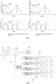
- the modulator 203 may perform a modulation on the output light beam of the light source so as to generate the light beam with a time-varying wavelength or a time-varying amplitude modulation frequency, of which the types of modulation may include any one of chirped amplitude modulation (CAM) or frequency modulation continuous wave (FMCW), which is shown in FIG. 5 .
- the beam splitting unit 204 may split the modulated light beam respectively into the reference light and the signal light.
- the modulator 203 may include but not limited to Mach-Zehnder Interferometer (MZI), ring resonator interferometer, tunable optical attenuator, etc.
- the beam splitting unit 204 may include but not limited to a Y-branch, a star coupler, a multimode interference coupler (MMI), a directional coupler, a polarizing beamsplitter, a partially diffractive and partially transmissive waveguide grating, etc.
- the on-chip emission unit 102 includes an on-chip beam expansion structure and a diffraction structure.
- the on-chip beam expansion structure may shape the output signal light, then the signal light may be irradiated at a large angle of divergence by the diffraction structure and form the reflected signal light on the target object.
- the on-chip beam expansion structure may include any one of a thermal insulation inversely tapered waveguide, a planar waveguide concave reflection mirror, a planar waveguide lens based on a waveguide layer with a thickness that gradually changes, a micro-nano-structure based planar waveguide lens with a refractive index that gradually changes, a cascaded beam splitter and a star coupler.
- the diffraction structure may include a waveguide diffraction grating array or a planar waveguide grating.
- Each of the reception units in the reception array 103 may include a diffraction structure, a light combination assembly and a sensor.
- the reflected signal light may need to be processed by a corresponding guiding structure unit before entering the reception array 103.
- a Fourier lens 206 may focus the signal lights reflected in various directions respectively onto corresponding N reception units, thereby allowing each of the reception units to correspond to one angle of view of the target object so as to perform a detection on the shape and location of the target object.
- the signal light reflected at a large angle of divergence passes through the Fourier lens 206, which allows the signal lights reflected in various directions to be focused onto the corresponding reception units, thereby implementing one-to-one correspondence between the signal lights reflected in various directions and the reception units, which can improve the utilization rate of the reflected signal light, and be conducive to reducing the total power required by the ranging chip and extending the ranging distance.
- FIG. 6 shows a schematic diagram of the structure of an array coherent ranging chip provided by an embodiment of the present application.
- the modulated light source unit 101 is composed of a light source 202, a modulator 203 and a beam splitting unit 204.
- the modulated light source unit 101 may include a signal generator (not shown).
- the light source 202 may be a narrow linewidth laser device with a central wavelength of 1550 nm.
- the output light of the laser device may be modulated by the modulator 203, of which the modulation frequency is distributed as a triangular wave over time.
- the modulated light beam may be divided into two paths by the beam splitting unit 204, wherein one path may be the signal light that is emitted from the on-chip emission unit 102 (which is a grating in this embodiment of the present application) and irradiates towards the target object at a large angle of divergence, whereas the other path may be the reference light that passes through the reception array and enter each of the reception units respectively as the reference light.
- the reception array may include a beam splitting region 301 and a reception module 302.
- the beam splitting region 301 may be composed of beam splitting units which sequentially and evenly splits and transmits the reference light into each of the reception units of the reception module 302 in order to be used as the intrinsic light.
- the reception module 302 may be composed of M ⁇ N reception units 303.
- the on-chip emission unit 102 may perform, by adding an off-chip scanning device such as a MEMS micromirror or a transmission/reflection optical phased array (OPA), a scanning of the direction of emission of the signal light so as to implement dynamic partial-angle-of-view ranging.
- an off-chip scanning device such as a MEMS micromirror or a transmission/reflection optical phased array (OPA)
- OPA transmission/reflection optical phased array
- the structure of the reception unit 303 is composed of a diffraction structure 601, a light combination assembly 602, and a sensor 603.
- the diffraction structure 601 may receive the reflected signal light and guide the reflected light of a specific angle into an input end of the light combination assembly in correspondence with a specific unit in the reception array.
- the light combination assembly 602 may receive the reflected signal light as well as the reference light that has been input, combine the reference light and the reflected signal light into a composite signal, and divide the composite signal into the first detection signal and the second detection signal.
- the sensor 603 may be configured to receive the first detection signal and the second detection signal, convert the first detection signal and the second detection signal into electric signals, and output a difference between the electric signals to obtain the ranging signals.
- the one-to-one correspondence between the signal lights reflected in various directions and the M ⁇ N reception units 303 may be implemented by performing proper adjustments on the parameters of the gratings in the M ⁇ N reception units 303, thereby inputting the signal lights reflected in various directions into corresponding light combination assemblies 602 to mix the reflected signal light with the reference light. Then, a difference value processing may be performed by the sensor 603 to obtain the signals of distance and location.
- the sensor may be composed of 2 ⁇ 2 balanced detectors, and optical sensing devices in the 2 ⁇ 2 balanced detection arrays may be based on SPAD, APD, PIN photoelectric sensor.
- the light combination assembly 602 and the sensor 603 in the reception array of the chip may be integrated on the same chip, or otherwise, alternatively, be integrated separately on two chips, with an optic or electric connection therebetween.
- the functionality of the light combination assembly 602 may convert the incident reference light E Lo and the reflected light E S e i ⁇ of the corresponding angle to form four mixed signals with amplitudes respectively of 2 E S ⁇ E LO / 2 , 2 E S + E LO / 2 , 2 E S + iE LO / 2 and 2 E S ⁇ iE LO / 2 as output, wherein the first two and the last two of the four mixed signals may each form a group of signals respectively with phase differences of 0 degree and 180 degrees.
- the four signals output by the light combination assembly may be received by the sensor 603 of the reception unit, wherein the two groups of signals respectively with phase differences of 0 degree and 180 degrees may each form a balanced detection by a signal circuit of the sensor.
- the low-frequency component of the intensity difference between the two groups of output signals of the light combination assembly is directly proportional to E L 0 E S cos ( ⁇ ), and thus the signal intensity difference is a sinusoidal signal of which the amplitude is directly proportional to the amplitude of the intrinsic light and the amplitude of the signal light, as well.
- the movement of the target object may superpose Doppler shift onto the reflected signal, which may lead to frequency differences at the frequency rising edge and at the frequency falling edge in the signal that is generated by the coherence with and the superposition onto the reference light, which is shown in FIG. 5 .
- the incident light signals may be converted into electric signals by the sensor 603.
- the high frequency component and the direct-current component may be filtered, then the two groups of signals may be amplified and output, and then the difference values of signals respectively from the two groups of signals may be squared and summed so as to obtain an output signal, thereby the impact of phase on signals can be removed by filtering.
- the signal processing unit may receive ranging signals output by the array coherent ranging chip and calculate a distance from the target object by a spectrum analysis.
- Fig.7 shows a schematic diagram of the structure of an array coherent ranging chip provided by an embodiment of the present application.
- the modulated light source unit 101 is composed of a light source 202, a modulator 203 and a beam splitting unit 204.
- the output light of the light source 202 may be modulated by a modulator 203. Then, the modulated light beam may be divided into two paths by the beam splitting unit 204, wherein one path may be the signal light that is emitted from the on-chip emission unit 102 and irradiates towards the target object at a large angle of divergence, whereas the other path may be the reference light that passes through the reception array and enter each of the reception units respectively as the reference light.
- the reception array may include a beam splitting region 301 and a reception module 302.
- the beam splitting region 301 may be composed of multiple beam splitting units which sequentially and evenly splits and transmits the reference light into each of the reception units of the reception module 302 in order to be used as the intrinsic light.
- the reception module 302 may be composed of M ⁇ N reception units 303.
- the on-chip emission unit 102 may be composed of optical phased arrays (OPAs).
- OPAs optical phased arrays
- the signal light split from the beam splitting unit 204 may pass through a waveguide and enter the beam splitting region 704 of the phased array, and then enter the phased region 703 of the phased array, which is connected to each channel of the phased array, thereby separately controlling the phase distribution in each channel via a phase modulator 705 in each channel of the phased region.
- the deflection in one direction of the output unit 702 of the optical phased array may be implemented by controlling the phase distribution among the respective channels of the optical phased array.
- the deflection of the signal light in the other direction may be implemented. Accordingly, the scanning functionality of the coherent ranging chip in two dimensions may be implemented.
- the number of channels and the parameters of structure of the optical phased array high-quality light beam can be easily implemented, the sidelobe suppression can be achieved, and as compared to a MEMS micromirror, the optical phased array can be integrated on a ranging chip more easily.
- the structure of the reception unit 303 is composed of a diffraction structure 601, a light combination assembly 602, and a sensor 603.
- the diffraction structure 601 may receive the reflected signal light and guide the reflected light of a specific angle into an input end of the light combination assembly in correspondence with a specific unit in the reception array.
- the light combination assembly 602 may receive the reflected signal light and as well as the reference light that has been input, combine the reference light and the reflected signal light into a composite signal, and divide the composite signal into the first detection signal and the second detection signal.
- the sensor 603 may be configured to receive the first detection signal and the second detection signal, convert the first detection signal and the second detection signal into electric signals, and output a difference between the electric signals to obtain the ranging signals. Then, the signal processing unit may receive the ranging signal output by the array coherent ranging chip and calculate a distance from the target object by a spectrum analysis.
Landscapes
- Engineering & Computer Science (AREA)
- Physics & Mathematics (AREA)
- Computer Networks & Wireless Communication (AREA)
- General Physics & Mathematics (AREA)
- Radar, Positioning & Navigation (AREA)
- Remote Sensing (AREA)
- Electromagnetism (AREA)
- Optical Radar Systems And Details Thereof (AREA)
Applications Claiming Priority (2)
| Application Number | Priority Date | Filing Date | Title |
|---|---|---|---|
| CN202011045282.9A CN112051582A (zh) | 2020-09-28 | 2020-09-28 | 一种阵列式相干测距芯片及其系统 |
| PCT/CN2020/127983 WO2022062105A1 (fr) | 2020-09-28 | 2020-11-11 | Puce de télémétrie cohérente en réseau et son système |
Publications (2)
| Publication Number | Publication Date |
|---|---|
| EP4220227A1 true EP4220227A1 (fr) | 2023-08-02 |
| EP4220227A4 EP4220227A4 (fr) | 2024-03-06 |
Family
ID=73605000
Family Applications (1)
| Application Number | Title | Priority Date | Filing Date |
|---|---|---|---|
| EP20954949.2A Pending EP4220227A4 (fr) | 2020-09-28 | 2020-11-11 | Puce de télémétrie cohérente en réseau et son système |
Country Status (3)
| Country | Link |
|---|---|
| EP (1) | EP4220227A4 (fr) |
| CN (1) | CN112051582A (fr) |
| WO (1) | WO2022062105A1 (fr) |
Families Citing this family (18)
| Publication number | Priority date | Publication date | Assignee | Title |
|---|---|---|---|---|
| CN113162685B (zh) * | 2021-02-23 | 2022-08-02 | 鹏城实验室 | 片上波前传感器、光芯片及通信设备 |
| CN112924953B (zh) * | 2021-03-10 | 2024-10-01 | 杭州洛微科技有限公司 | 一种光探测系统和方法、激光雷达系统 |
| CN113078956B (zh) * | 2021-03-10 | 2022-08-02 | 中国科学院紫金山天文台 | 基于相位光栅的太赫兹多波段相干接收系统 |
| US11409000B1 (en) * | 2021-04-15 | 2022-08-09 | Aeva, Inc. | Techniques for simultaneous determination of range and velocity with passive modulation |
| CN114002703B (zh) * | 2021-10-21 | 2025-06-06 | 扬州扬芯激光技术有限公司 | 一种三维成像的全固态激光雷达装置 |
| CN113671464B (zh) * | 2021-10-22 | 2022-02-18 | 杭州视光半导体科技有限公司 | 一种片上相干检测的扫描同轴面阵收发机 |
| CN114415190B (zh) * | 2021-12-30 | 2025-07-15 | 图达通智能科技(苏州)有限公司 | 一种激光雷达的收发装置 |
| TW202338397A (zh) * | 2022-03-30 | 2023-10-01 | 美商歐普微股份有限公司 | 高速干擾時間光檢測和測距系統及確定距離的方法與裝置 |
| CN114740617B (zh) * | 2022-04-08 | 2023-06-30 | 中国科学院光电技术研究所 | 一种大视场高分辨全固态光学扫描系统 |
| CN114935398A (zh) * | 2022-05-26 | 2022-08-23 | 安徽至博光电科技股份有限公司 | 一种大范围扫描测振的集成光学芯片及方法 |
| CN115224138B (zh) * | 2022-06-17 | 2023-12-08 | 浙江大学 | 一种水平拉通型锗硅雪崩光电探测器 |
| CN115128579A (zh) * | 2022-07-19 | 2022-09-30 | 国科光芯(海宁)科技股份有限公司 | 激光雷达芯片模组、激光雷达系统及激光探测方法 |
| CN115754982B (zh) * | 2022-10-31 | 2025-09-30 | 国网陕西省电力有限公司电力科学研究院 | 一种光子集成芯片、水土流失在线监测装置及方法 |
| CN116609269B (zh) * | 2023-05-15 | 2025-08-08 | 上海交通大学 | 基于光子芯片的sd-oct系统 |
| CN116660919A (zh) * | 2023-05-26 | 2023-08-29 | 深圳玩智商科技有限公司 | 一种多点激光测距装置及方法 |
| CN116593995A (zh) * | 2023-06-20 | 2023-08-15 | 广州导远电子科技有限公司 | 光信号接收装置及激光雷达 |
| CN117169893B (zh) * | 2023-11-02 | 2024-01-26 | 崂山国家实验室 | 激光致声跨空水下目标探测系统及方法 |
| CN119395663B (zh) * | 2024-09-20 | 2025-09-26 | 清华大学 | 光子集成芯片、应用光子集成芯片的激光雷达、探测方法 |
Family Cites Families (15)
| Publication number | Priority date | Publication date | Assignee | Title |
|---|---|---|---|---|
| EP3161520B1 (fr) * | 2014-06-27 | 2021-10-13 | HRL Laboratories, LLC | Lidar à balayage compressif |
| CN105842685B (zh) * | 2016-03-18 | 2019-02-12 | 浙江大华技术股份有限公司 | 一种多目标雷达探测方法 |
| WO2017223299A1 (fr) * | 2016-06-22 | 2017-12-28 | Massachusetts Institute Of Technology | Procédés et systèmes pour orientation de faisceau optique |
| CN107783128B (zh) * | 2016-08-25 | 2021-02-19 | 大连楼兰科技股份有限公司 | 基于毫米波雷达的固定翼无人机多目标防撞系统 |
| EP3523675B1 (fr) * | 2016-10-06 | 2025-12-17 | GM Global Technology Operations LLC | Système de lidar |
| JP7140784B2 (ja) * | 2017-03-01 | 2022-09-21 | ポイントクラウド インコーポレイテッド | モジュラー三次元光学検知システム |
| JP6743761B2 (ja) * | 2017-05-29 | 2020-08-19 | 株式会社デンソー | 測距センサ |
| US10838047B2 (en) * | 2018-04-17 | 2020-11-17 | Santec Corporation | Systems and methods for LIDAR scanning of an environment over a sweep of wavelengths |
| US20200116842A1 (en) * | 2018-10-12 | 2020-04-16 | Silc Technologies, Inc. | Optical switching in lidar systems |
| CN109991582B (zh) * | 2019-03-13 | 2023-11-03 | 上海交通大学 | 硅基混合集成激光雷达芯片系统 |
| CN110109083B (zh) * | 2019-05-05 | 2023-06-27 | 上海交通大学 | 基于一维光相控阵的三维扫描激光雷达 |
| CN110174661B (zh) * | 2019-05-10 | 2024-04-16 | 浙江大学 | 一种基于偏振复用的光学相控阵二维激光雷达扫描芯片 |
| CN110687518B (zh) * | 2019-09-30 | 2021-07-13 | 中国电子科技集团公司信息科学研究院 | 一种片上集成平衡探测接收系统和方法 |
| CN111596281B (zh) * | 2020-06-17 | 2020-11-13 | 中国电子科技集团公司信息科学研究院 | 三维集成平衡探测器接收装置以及集成方法 |
| CN212515027U (zh) * | 2020-09-28 | 2021-02-09 | 国科光芯(海宁)科技股份有限公司 | 一种阵列式相干测距芯片及其系统 |
-
2020
- 2020-09-28 CN CN202011045282.9A patent/CN112051582A/zh active Pending
- 2020-11-11 EP EP20954949.2A patent/EP4220227A4/fr active Pending
- 2020-11-11 WO PCT/CN2020/127983 patent/WO2022062105A1/fr not_active Ceased
Also Published As
| Publication number | Publication date |
|---|---|
| WO2022062105A1 (fr) | 2022-03-31 |
| EP4220227A4 (fr) | 2024-03-06 |
| CN112051582A (zh) | 2020-12-08 |
Similar Documents
| Publication | Publication Date | Title |
|---|---|---|
| EP4220227A1 (fr) | Puce de télémétrie cohérente en réseau et son système | |
| KR102705380B1 (ko) | 솔리드 스테이트 스펙트럼 스캐닝을 갖는 lidar 시스템 | |
| CN111880190B (zh) | 一种相干激光测距芯片及其系统 | |
| CN115639543B (zh) | 调频连续波激光雷达及自动驾驶设备 | |
| CN212515027U (zh) | 一种阵列式相干测距芯片及其系统 | |
| TWI801364B (zh) | 用於提供啾頻光束之半導體光子電路及方法 | |
| EP3956679B1 (fr) | Appareil et procédé de gestion de détection cohérente à partir de multiples ouvertures dans un système lidar | |
| US11899112B2 (en) | Laser radar device | |
| JP2021121810A (ja) | 空間プロファイリングの方法および空間プロファイリングシステム | |
| JP2022521459A (ja) | スペックル感度が低減されたlidarシステム | |
| CN113848540B (zh) | 一种面阵色散光谱感光组件、接收端以及激光雷达系统 | |
| CN113848537B (zh) | 一种色散光谱感光组件、接收端及激光雷达系统 | |
| JP7315154B2 (ja) | 距離及び速度測定装置 | |
| CN116973926A (zh) | 激光雷达 | |
| KR20220119049A (ko) | 솔리드 스테이트 빔 조향을 포함하는 고해상도 주파수 변조 연속파 라이다 | |
| CN117008134A (zh) | 相干激光雷达系统及探测方法 | |
| CN120215023B (zh) | 一种光子集成芯片及调频连续波激光雷达 | |
| US20240027582A1 (en) | Array coherent ranging chip and system thereof | |
| CN116087971B (zh) | 一种opa激光雷达 | |
| EP4375702A1 (fr) | Dispositif de balayage de mesure de plage lidar fmcw | |
| US20220236418A1 (en) | Lidar system comprising an interferential diffractive element and lidar imaging method | |
| US20240168223A1 (en) | Photonic integrated circuit for multiple frequency shifting of light | |
| CN120214750A (zh) | 激光雷达及其探测方法、收发装置 | |
| CN120993428A (zh) | 激光雷达 | |
| CN120802215A (zh) | 双轴扫描装置及双轴扫描系统 |
Legal Events
| Date | Code | Title | Description |
|---|---|---|---|
| STAA | Information on the status of an ep patent application or granted ep patent |
Free format text: STATUS: THE INTERNATIONAL PUBLICATION HAS BEEN MADE |
|
| PUAI | Public reference made under article 153(3) epc to a published international application that has entered the european phase |
Free format text: ORIGINAL CODE: 0009012 |
|
| STAA | Information on the status of an ep patent application or granted ep patent |
Free format text: STATUS: REQUEST FOR EXAMINATION WAS MADE |
|
| 17P | Request for examination filed |
Effective date: 20230419 |
|
| AK | Designated contracting states |
Kind code of ref document: A1 Designated state(s): AL AT BE BG CH CY CZ DE DK EE ES FI FR GB GR HR HU IE IS IT LI LT LU LV MC MK MT NL NO PL PT RO RS SE SI SK SM TR |
|
| DAV | Request for validation of the european patent (deleted) | ||
| DAX | Request for extension of the european patent (deleted) | ||
| A4 | Supplementary search report drawn up and despatched |
Effective date: 20240201 |
|
| RIC1 | Information provided on ipc code assigned before grant |
Ipc: G01S 17/36 20060101ALN20240126BHEP Ipc: G01S 7/4912 20200101ALN20240126BHEP Ipc: G01S 7/481 20060101ALI20240126BHEP Ipc: G01S 7/4914 20200101ALI20240126BHEP Ipc: G01S 7/4911 20200101ALI20240126BHEP Ipc: G01S 17/32 20200101AFI20240126BHEP |
|
| STAA | Information on the status of an ep patent application or granted ep patent |
Free format text: STATUS: EXAMINATION IS IN PROGRESS |
|
| 17Q | First examination report despatched |
Effective date: 20250714 |