EP4220705A1 - Wärmeableitungsanordnung zur reduzierung von elektromagnetischem rauschen eines chips, chipgehäuseanordnung und elektronische vorrichtung - Google Patents
Wärmeableitungsanordnung zur reduzierung von elektromagnetischem rauschen eines chips, chipgehäuseanordnung und elektronische vorrichtung Download PDFInfo
- Publication number
- EP4220705A1 EP4220705A1 EP21885093.1A EP21885093A EP4220705A1 EP 4220705 A1 EP4220705 A1 EP 4220705A1 EP 21885093 A EP21885093 A EP 21885093A EP 4220705 A1 EP4220705 A1 EP 4220705A1
- Authority
- EP
- European Patent Office
- Prior art keywords
- ring
- chip
- heat dissipation
- heat sink
- suppression
- Prior art date
- Legal status (The legal status is an assumption and is not a legal conclusion. Google has not performed a legal analysis and makes no representation as to the accuracy of the status listed.)
- Pending
Links
Images






Classifications
-
- H—ELECTRICITY
- H10—SEMICONDUCTOR DEVICES; ELECTRIC SOLID-STATE DEVICES NOT OTHERWISE PROVIDED FOR
- H10W—GENERIC PACKAGES, INTERCONNECTIONS, CONNECTORS OR OTHER CONSTRUCTIONAL DETAILS OF DEVICES COVERED BY CLASS H10
- H10W40/00—Arrangements for thermal protection or thermal control
- H10W40/20—Arrangements for cooling
- H10W40/22—Arrangements for cooling characterised by their shape, e.g. having conical or cylindrical projections
- H10W40/226—Arrangements for cooling characterised by their shape, e.g. having conical or cylindrical projections characterised by projecting parts, e.g. fins to increase surface area
-
- H—ELECTRICITY
- H10—SEMICONDUCTOR DEVICES; ELECTRIC SOLID-STATE DEVICES NOT OTHERWISE PROVIDED FOR
- H10W—GENERIC PACKAGES, INTERCONNECTIONS, CONNECTORS OR OTHER CONSTRUCTIONAL DETAILS OF DEVICES COVERED BY CLASS H10
- H10W42/00—Arrangements for protection of devices
- H10W42/20—Arrangements for protection of devices protecting against electromagnetic or particle radiation, e.g. light, X-rays, gamma-rays or electrons
-
- H—ELECTRICITY
- H10—SEMICONDUCTOR DEVICES; ELECTRIC SOLID-STATE DEVICES NOT OTHERWISE PROVIDED FOR
- H10W—GENERIC PACKAGES, INTERCONNECTIONS, CONNECTORS OR OTHER CONSTRUCTIONAL DETAILS OF DEVICES COVERED BY CLASS H10
- H10W42/00—Arrangements for protection of devices
- H10W42/60—Arrangements for protection of devices protecting against electrostatic charges or discharges, e.g. Faraday shields
-
- H—ELECTRICITY
- H10—SEMICONDUCTOR DEVICES; ELECTRIC SOLID-STATE DEVICES NOT OTHERWISE PROVIDED FOR
- H10W—GENERIC PACKAGES, INTERCONNECTIONS, CONNECTORS OR OTHER CONSTRUCTIONAL DETAILS OF DEVICES COVERED BY CLASS H10
- H10W74/00—Encapsulations, e.g. protective coatings
- H10W74/10—Encapsulations, e.g. protective coatings characterised by their shape or disposition
- H10W74/111—Encapsulations, e.g. protective coatings characterised by their shape or disposition the semiconductor body being completely enclosed
- H10W74/114—Encapsulations, e.g. protective coatings characterised by their shape or disposition the semiconductor body being completely enclosed by a substrate and the encapsulations
-
- H—ELECTRICITY
- H10—SEMICONDUCTOR DEVICES; ELECTRIC SOLID-STATE DEVICES NOT OTHERWISE PROVIDED FOR
- H10W—GENERIC PACKAGES, INTERCONNECTIONS, CONNECTORS OR OTHER CONSTRUCTIONAL DETAILS OF DEVICES COVERED BY CLASS H10
- H10W76/00—Containers; Fillings or auxiliary members therefor; Seals
- H10W76/40—Fillings or auxiliary members in containers, e.g. centering rings
-
- H—ELECTRICITY
- H10—SEMICONDUCTOR DEVICES; ELECTRIC SOLID-STATE DEVICES NOT OTHERWISE PROVIDED FOR
- H10W—GENERIC PACKAGES, INTERCONNECTIONS, CONNECTORS OR OTHER CONSTRUCTIONAL DETAILS OF DEVICES COVERED BY CLASS H10
- H10W76/00—Containers; Fillings or auxiliary members therefor; Seals
- H10W76/60—Seals
-
- H—ELECTRICITY
- H10—SEMICONDUCTOR DEVICES; ELECTRIC SOLID-STATE DEVICES NOT OTHERWISE PROVIDED FOR
- H10W—GENERIC PACKAGES, INTERCONNECTIONS, CONNECTORS OR OTHER CONSTRUCTIONAL DETAILS OF DEVICES COVERED BY CLASS H10
- H10W40/00—Arrangements for thermal protection or thermal control
- H10W40/20—Arrangements for cooling
- H10W40/22—Arrangements for cooling characterised by their shape, e.g. having conical or cylindrical projections
-
- H—ELECTRICITY
- H10—SEMICONDUCTOR DEVICES; ELECTRIC SOLID-STATE DEVICES NOT OTHERWISE PROVIDED FOR
- H10W—GENERIC PACKAGES, INTERCONNECTIONS, CONNECTORS OR OTHER CONSTRUCTIONAL DETAILS OF DEVICES COVERED BY CLASS H10
- H10W76/00—Containers; Fillings or auxiliary members therefor; Seals
- H10W76/60—Seals
- H10W76/63—Seals characterised by their shape or disposition, e.g. between cap and walls of a container
-
- H—ELECTRICITY
- H10—SEMICONDUCTOR DEVICES; ELECTRIC SOLID-STATE DEVICES NOT OTHERWISE PROVIDED FOR
- H10W—GENERIC PACKAGES, INTERCONNECTIONS, CONNECTORS OR OTHER CONSTRUCTIONAL DETAILS OF DEVICES COVERED BY CLASS H10
- H10W90/00—Package configurations
- H10W90/701—Package configurations characterised by the relative positions of pads or connectors relative to package parts
- H10W90/731—Package configurations characterised by the relative positions of pads or connectors relative to package parts of die-attach connectors
- H10W90/736—Package configurations characterised by the relative positions of pads or connectors relative to package parts of die-attach connectors between a chip and a stacked lead frame, conducting package substrate or heat sink
Definitions
- This application relates to the technical field of chips, and in particular, to a heat dissipation assembly for reducing electromagnetic noise of a chip, a chip packaging assembly, and an electronic device.
- bare die packaging gradually becomes a mainstream process of packaging the chip with high power consumption, to improve a heat dissipation benefit of the chip.
- a chip in a packaging assembly based on a bare die packaging process has relatively high externally radiated power. Consequently, the chip packaging assembly has relatively high electromagnetic noise.
- An objective of this application is to provide a heat dissipation assembly for reducing electromagnetic noise of a chip, a chip packaging assembly, and an electronic device, to resolve a problem that an existing chip packaging assembly has relatively high electromagnetic noise.
- the heat dissipation assembly includes a heat sink, a seal ring, and a suppression ring.
- the suppression ring is connected between the seal ring and the heat sink, and is configured to surround a chip.
- the heat dissipation assembly is configured to form an enclosed space together with a substrate carrying the chip, so that the chip is located in the enclosed space.
- the suppression ring is configured to shield an electromagnetic wave radiated by the chip.
- the heat dissipation assembly can ensure that a chip packaging assembly in which the heat dissipation assembly is used has relatively low electromagnetic noise while ensuring a heat dissipation benefit.
- the corresponding chip packaging assembly still maintains a relatively good electromagnetic noise suppression effect in a high frequency range above 20 GHz, so that radiated power of an electromagnetic wave in the high frequency range is still kept relatively low, to reduce electromagnetic pollution and a possibility of crosstalk between the chip packaging assembly and a radio frequency circuit.
- the suppression ring is located on a side that is of the seal ring and that faces the heat sink.
- the heat dissipation assembly can suppress the electromagnetic wave radiated by the chip to outside of the chip packaging assembly while meeting a heat dissipation requirement of the chip packaging assembly, to reduce electromagnetic noise of the chip packaging assembly.
- the heat sink includes a heat sink body and a ring-shaped support.
- the ring-shaped support is located on a side of the heat sink body and spaced from the seal ring.
- the suppression ring is partially or completely sandwiched between the ring-shaped support and the seal ring.
- the suppression ring includes a first ring-shaped part and a second ring-shaped part.
- the first ring-shaped part is sandwiched between the ring-shaped support and the seal ring.
- the second ring-shaped part is sandwiched between the heat sink body and the seal ring.
- the suppression ring is connected to the seal ring and the heat sink without a gap. In this way, there is no gap between the seal ring, the suppression ring, and the heat sink, to improve a shielding effect of the heat dissipation assembly on the electromagnetic wave radiated by the chip.
- the suppression ring is a flexible conductive gasket.
- the conductive gasket is sandwiched between the seal ring and the heat sink through elastic deformation.
- the suppression ring has specific elasticity. Based on this, while shielding the electromagnetic wave, the suppression ring may further serve as a cushion to protect the chip, to reduce pressure borne by the chip.
- the conductive gasket includes an elastic inner core and a conductive outer layer.
- the conductive outer layer is wrapped around the elastic inner core.
- the conductive gasket may have specific elasticity, to implement good bonding.
- the conductive gasket may be electrically connected to the heat sink and the seal ring, to ensure the effect of shielding the electromagnetic wave radiated by the chip.
- the elastic inner core is made of a foam material
- the conductive outer layer is made of conductive fiber cloth.
- the foam material may be, for example, a material having specific elasticity, such as polyurethane.
- the conductive fiber cloth may be, for example, a material having high electrical conductivity, such as nickel/copper (Ni/Cu).
- the conductive gasket is conductive foam. It should be understood that a conductive sponge also has electrical conductivity and compressibility, and can implement good bonding with the seal ring and the heat sink and shield the electromagnetic wave.
- the heat dissipation assembly includes a heat sink, a seal ring, and a suppression ring.
- the suppression ring is located between the seal ring and the heat sink, and is configured to surround a chip.
- the heat dissipation assembly is configured to form an enclosed space together with a substrate carrying the chip, so that the chip is located in the enclosed space.
- the suppression ring is configured to absorb an electromagnetic wave radiated by the chip. It should be understood that the suppression ring in this embodiment may be connected to at least one of the seal ring and the heat sink. That is, there may be a specific gap between the seal ring, the suppression ring, and the heat sink.
- a chip packaging assembly in which the heat dissipation assembly is used can have relatively low electromagnetic noise.
- the chip packaging assembly still maintains a relatively good electromagnetic noise suppression effect in a high frequency range above 20 GHz, so that radiated power of an electromagnetic wave in the high frequency range is still kept relatively low, to reduce electromagnetic pollution and a possibility of crosstalk between the chip packaging assembly and a radio frequency circuit.
- the suppression ring is located on a side that is of the seal ring and that faces the heat sink.
- the heat dissipation assembly can suppress the electromagnetic wave radiated by the chip to outside of the chip packaging assembly while meeting a heat dissipation requirement of the chip packaging assembly, to reduce electromagnetic noise of the chip packaging assembly.
- the heat sink includes a heat sink body and a ring-shaped support.
- the ring-shaped support is located on a side of the heat sink body and spaced from the seal ring.
- the suppression ring is partially or completely located between the ring-shaped support and the seal ring.
- the suppression ring includes a first ring-shaped part and a second ring-shaped part.
- the first ring-shaped part is located between the ring-shaped support and the seal ring.
- the second ring-shaped part is located between the heat sink body and the seal ring.
- the suppression ring is a ring-shaped mechanical part made of a wave-absorbing material.
- the wave-absorbing material may be, for example, graphite, graphene, carbon fiber, magnetic ceramic, or a conductive polymer.
- the first ring-shaped part is a conductive gasket; or the first ring-shaped part is a ring-shaped mechanical part made of a wave-absorbing material.
- the second ring-shaped part is a conductive gasket; or the first ring-shaped part is a ring-shaped mechanical part made of a wave-absorbing material.
- the second ring-shaped part may further reduce pressure borne by the chip.
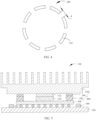
- the seal ring is an enclosed ring-shaped structure; or the seal ring includes a plurality of substructures, and the plurality of substructures are spaced apart on a periphery of the chip.
- the heat dissipation assembly includes a heat sink and a suppression ring.
- the suppression ring is located on a side of the heat sink, and is configured to surround a chip.
- the heat dissipation assembly is configured to form an enclosed space together with a substrate carrying the chip, so that the chip is located in the enclosed space.
- the suppression ring is a conductive gasket, or the suppression ring is a ring-shaped mechanical part made of a wave-absorbing material.
- the chip packaging assembly includes a chip, a substrate, and the heat dissipation assembly for reducing electromagnetic noise of a chip in the foregoing embodiments.
- the chip is disposed on the substrate.
- the substrate and the heat dissipation assembly jointly form an enclosed space.
- the chip is located in the enclosed space.
- the electronic device includes the chip packaging assembly for reducing electromagnetic noise in the foregoing embodiment.
- the electronic device may be a router or a switch.
- the heat dissipation assembly when used in the chip packaging assembly, through cooperation between the suppression ring and a related structure, the heat dissipation assembly can suppress the electromagnetic wave radiated by the chip to the outside of the chip packaging assembly while meeting the heat dissipation requirement, to reduce the electromagnetic noise of the chip packaging assembly and the possibility of crosstalk between the chip packaging assembly and the radio frequency circuit.
- the chip As an integration level of a chip increases, the chip has a stronger processing capability. However, power consumption of the chip also sharply increases. It should be understood that a chip with higher power consumption generates more heat during operation, and the heat needs to be dissipated in time. In recent years, to improve a heat dissipation benefit of a chip, a metal lid (Lid) packaging process is gradually replaced by a bare die (Die) packaging process in the industry. The chip is packaged to form a chip packaging assembly through bare die packaging.
- Lid metal lid
- Die bare die
- a chip 110 is disposed on a substrate 100, and a seal ring (Seal Ring) 120 surrounds the chip 110.
- a metal lid 122 originally covering the chip 110 is removed. Because the metal lid 122 covering the chip 110 is removed, the chip 110 may be connected to a heat sink 130 through a thermal interface material (TIM, Thermal Interface Material) 112, and directly conduct heat to the heat sink 130 to implement heat dissipation. In this way, a heat dissipation benefit of the bare die packaging-based chip packaging assembly is improved, and a heat dissipation requirement of the chip can be met.
- TIM Thermal Interface Material
- the seal ring 120 surrounds the chip 110, the seal ring 120 cannot provide good shielding between the substrate 100 and the heat sink 130 due to factors such as a component process tolerance, a packaging requirement, and a subsequent test. This results in a gap between the seal ring 120 and the heat sink 130, and/or is prone to a gap between the substrate 100 and the seal ring 120.
- the chip 110 packaged through bare die packaging is easier to radiate an electromagnetic wave to outside of the chip packaging assembly.
- the radiated electromagnetic wave is electromagnetic noise.
- An electromagnetic wave with a higher frequency has a smaller wavelength.
- An electromagnetic wave in a high frequency range is easier to be radiated to outside through a narrow gap than an electromagnetic wave in a low frequency range. For example, it is found through simulation that in a high frequency range of 20 GHz to 35 GHz, radiated power of electromagnetic noise externally radiated by the bare die packaging-based chip packaging assembly increases by 5 dB to 10 dB in comparison with the metal lid packaging-based chip packaging assembly. Based on this, in the bare die packaging-based chip packaging assembly, it is more difficult to suppress the electromagnetic wave in the high frequency range.
- the radiated electromagnetic wave is easy to cause electromagnetic pollution and interference to an external circuit or signal while forming electromagnetic noise.
- the electromagnetic noise externally radiated by the chip packaging assembly has a risk of interfering with a radio frequency circuit; or an electromagnetic wave externally radiated by a radio frequency circuit also has a risk of interfering with the chip packaging assembly.
- the crosstalk causes specific impact on performance of the electronic device. For example, in a frequency range of 5 GHz to 6 GHz, electromagnetic noise externally radiated by the chip packaging assembly is easy to cause crosstalk to the radio frequency circuit, and affects normal operation of the radio frequency circuit; or an electromagnetic wave externally radiated by the radio frequency circuit and a corresponding antenna is easy to cause crosstalk to the chip packaging assembly, and affects normal operation of the chip packaging assembly.
- the bare die packaging-based chip packaging assembly has problems such as high electromagnetic noise and radio frequency interference.
- Embodiments of this application provide a heat dissipation assembly, a chip packaging assembly, and an electronic device in which the chip packaging assembly is used.
- the heat dissipation assembly in each embodiment is integrated into the chip packaging assembly to serve as a part of the chip packaging assembly, but is not limited thereto. In some other implementations, the heat dissipation assembly may alternatively be an independent assembly.
- the heat dissipation assembly is assembled with structures such as a substrate and a chip to form the chip packaging assembly.
- the electronic device may be, for example, a router or a switch. It should be understood that the electronic device may further include structures such as a radio frequency circuit and a filter. This is not limited.
- an embodiment of this application provides a chip packaging assembly 11a.
- the chip packaging assembly 11a includes a substrate 100, a chip 110, and a heat dissipation assembly 200.
- the heat dissipation assembly 200 includes a seal ring 120, a suppression ring 140, and a heat sink 130.
- the seal ring 120 may be an enclosed ring-shaped structure.
- a cross-sectional shape of the seal ring 120 may be a rectangle or a circle. It should be understood that the cross-sectional shape of the seal ring 120 is not limited in this application.
- the cross-sectional shape of the seal ring 120 may be adaptively designed based on an actual structure requirement of the chip packaging assembly (11a or 11b). This is not limited.
- the cross-sectional shape of the seal ring 120 may alternatively be a trapezoid, a D-shape, or the like.
- the seal ring 120 may include a plurality of substructures 121.
- the plurality of substructures 121 are spaced apart on a periphery of the chip 121.
- a distance d between every two adjacent substructures 121 is a quarter of a wavelength corresponding to a frequency of an electromagnetic wave to be suppressed. In this way, electromagnetic radiation of the corresponding frequency can be suppressed.
- the suppression ring 140 surrounds the chip 110 and may shield an electromagnetic wave radiated by the chip 110. This reduces electromagnetic noise of the chip packaging assembly 11a, to reduce electromagnetic pollution. In some other embodiments, the suppression ring 140 may absorb an electromagnetic wave radiated by the chip 110. This can also reduce electromagnetic noise, to reduce electromagnetic pollution. It should be understood that the suppression ring 140 provided in embodiments of this application may be flexible (for example, a conductive gasket mentioned below) or rigid (for example, a ring-shaped mechanical part made of a wave-absorbing material mentioned below). The suppression ring 140 can suppress electromagnetic wave radiation. Suppressing electromagnetic wave radiation may be, for example, shielding an electromagnetic wave or absorbing an electromagnetic wave. In some embodiments, a material of the suppression ring may be, for example, as described below.
- the suppression ring 140 is located on a side that is of the seal ring 120 and that is away from the substrate 100. That is, the suppression ring 140 is connected between the seal ring 120 and the heat sink 130, to reduce or even eliminate an original gap between the seal ring 120 and the heat sink 130. It should be understood that the substrate 100 and the heat dissipation assembly 200 jointly form an enclosed space.
- the chip 110 is disposed in the enclosed space.
- a material of the heat sink 130 may be, for example, a metal or a nonmetallic heat conducting material.
- the electromagnetic wave radiated by the chip 110 in the enclosed space to outside of the chip packaging assembly 11a can be suppressed through cooperation between the suppression ring 140, the heat sink 130, and the seal ring 120, to reduce the electromagnetic noise of the chip packaging assembly 11a and a possibility of crosstalk between the chip packaging assembly 11a and a radio frequency circuit.
- chip packaging assembly in each embodiment is merely described by using the radio frequency circuit as an example, but it is not limited to that the chip packaging assembly is only for the radio frequency circuit.
- the chip packaging assembly in each embodiment may alternatively reduce a possibility of crosstalk with another chip packaging assembly. This is not limited.
- the suppression ring 140 may be fastened through adhesive backing; or the suppression ring 140 may be fastened through adhesive dispensing. This is not limited.
- the suppression ring 140 is fastened to the seal ring 120 through adhesive backing.
- the heat sink 130 is fastened through a screw or the like.
- the suppression ring 140 is located between the seal ring 120 and the heat sink 130.
- the suppression ring is flexible, the suppression ring may be sandwiched between the seal ring and the heat sink through elastic deformation, to seal the gap between the seal ring and the heat sink. If the suppression ring is rigid, an installation height of the heat sink may be controlled, so that there is a relatively small gap or no gap between the seal ring, the suppression ring, and the heat sink, to ensure an electromagnetic wave suppression effect.
- the suppression ring 140 is disposed between the seal ring 120 and the heat sink 130, so that a part, of the electromagnetic wave radiated by the chip 110, in a high frequency range (for example, 20 GHz to 35 GHz) is also difficult to be radiated to the outside. Therefore, the chip packaging assembly 11a in each embodiment may have a better electromagnetic noise suppression effect.
- the electromagnetic noise of the chip packaging assembly 11a can be reduced while a heat dissipation benefit of the chip 110 is ensured, to ensure normal operation of the chip packaging assembly 11a.
- the heat sink may further have a boss (not shown in the figure).
- the boss protrudes toward the chip and the substrate.
- the heat sink having the boss may be more easily in contact with the chip, to conduct heat dissipated by the chip.
- the suppression ring 140 is a conductive gasket.
- the conductive gasket has specific elasticity and can be compressed to some extent. Based on this, a compression rate of the conductive gasket is controlled, so that the conductive gasket can maintain good bonding with the seal ring 120 and the heat sink 130 through elastic deformation, to maximally eliminate the gap between the heat sink 130 and the seal ring 120. This reduces a possibility that the electromagnetic wave radiated by the chip 110 penetrates to the outside.
- the conductive gasket may be connected between the seal ring 120 and the heat sink 130 without a gap, to eliminate the original gap between the seal ring 120 and the heat sink 130.
- an enclosed space is formed among the substrate 100, the seal ring 120, the conductive gasket, and the heat sink 130. In this way, it is more difficult for the electromagnetic wave radiated by the chip 110 to penetrate to the outside, so that the chip packaging assembly 11a has a better electromagnetic noise suppression effect.
- the conductive gasket is sandwiched between the seal ring 120 and the heat sink 130, and is away from the substrate 100.
- the compression rate of the conductive gasket is controlled to be 40% by controlling a distance between the heat sink 130 and the substrate 100.
- the conductive gasket is stably fastened between the seal ring 120 and the heat sink 130 through elastic deformation. In this way, the conductive gasket has specific resilience, and the gap between the seal ring 120 and the heat sink 130 can be maximally eliminated.
- the conductive gasket may further serve as a cushion to protect the chip 110 during installation of the heat sink 130, to reduce pressure borne by the chip 110. It should be understood that when the heat sink 130 is fastened through the screw or the like, the heat sink 130 gradually presses the conductive gasket and makes the conductive gasket be compressed as the distance between the heat sink 130 and the substrate 100 decreases. Because the conductive gasket has resilience to return to an initial state, the resilience may reduce a force applied by the heat sink 130 on the chip 110, so that the pressure borne by the chip can be reduced.
- the conductive gasket includes an elastic inner core and a conductive outer layer.
- the conductive outer layer is wrapped around the elastic inner core.
- the conductive gasket has specific elasticity, to implement good bonding.
- the conductive gasket may be electrically connected to structures such as the heat sink 130 and the seal ring 120, to ensure an effect of shielding the electromagnetic wave radiated by the chip 110.
- the elastic inner core is made of a foam material.
- the foam material may be, for example, a material having specific elasticity, such as polyurethane.
- the conductive outer layer is made of conductive fiber cloth.
- the conductive fiber cloth may be, for example, a material having high electrical conductivity, such as nickel/copper (Ni/Cu).
- the conductive gasket may alternatively be a conductive sponge.
- the conductive sponge also has electrical conductivity and compressibility, and can implement good bonding with the seal ring 120 and the heat sink 130 and shield electromagnetic waves. It should be understood that a compression rate of the conductive sponge is higher than that of the conductive gasket including the elastic inner core and the conductive outer layer. For example, the compression rate of the conductive gasket is 30% to 50%, and the compression rate of the conductive sponge is 40% to 60%.
- the conductive sponge may have a larger size to ensure good bonding between the seal ring 120, the conductive sponge, and the heat sink 130.
- the suppression ring 140 is a ring-shaped mechanical part made of a wave-absorbing material, and is located between the seal ring 120 and the heat sink 130, to absorb and attenuate the electromagnetic wave radiated by the chip 110. It should be understood that, different from the conductive gasket, the ring-shaped mechanical part may be disposed on a side that is of the seal ring 120 and that faces the heat sink 130; or the ring-shaped mechanical part may be disposed on a side that is of the heat sink 130 and that faces the seal ring 120.
- an embodiment of this application provides a chip packaging assembly 11b.
- a suppression ring 140 of a heat dissipation assembly 200 is a ring-shaped mechanical part made of a wave-absorbing material.
- the ring-shaped mechanical part may not be in contact with a heat sink 130. That is, there may be a specific gap between the ring-shaped mechanical part and the heat sink 130.
- a formed enclosed space may have a specific gap, and does not need to be completely enclosed.
- the ring-shaped mechanical part when used in the chip packaging assembly (11a or 11b) in each embodiment, based on an absorption and attenuation effect of the ring-shaped mechanical part on electromagnetic waves, the electromagnetic wave radiated by the chip 110 is absorbed and attenuated by the ring-shaped mechanical part when passing through the gap.
- the ring-shaped mechanical part may convert electromagnetic energy into thermal energy or energy in another form by absorbing and attenuating the electromagnetic wave radiated by the chip 110, to consume the electromagnetic energy. This reduces radiated power of the electromagnetic wave externally radiated by the chip 110, to reduce electromagnetic noise.
- the ring-shaped mechanical part when the ring-shaped mechanical part is located on the side that is of the heat sink 130 and that faces the seal ring 120, there may also be a specific gap between the ring-shaped mechanical part and the seal ring 120. This is not limited.
- the wave-absorbing material may be, for example, graphite, graphene, carbon fiber, magnetic ceramic, or a conductive polymer.
- the suppression ring in each embodiment may alternatively be the ring-shaped mechanical part to achieve a similar effect of reducing electromagnetic noise.
- the ring-shaped mechanical part does not need to completely seal a gap between the seal ring and the heat sink. That is, after the heat sink is installed, there may be a specific gap between the heat sink, the ring-shaped mechanical part, and the seal ring.
- the electromagnetic wave radiated by the chip it is difficult for the electromagnetic wave radiated by the chip to penetrate through the gap to the outside. This can also reduce the electromagnetic noise of the chip packaging assembly, to ensure normal operation of the chip packaging assembly.
- a shape of the suppression ring 140 may be, for example, a circular ring, a hexagonal ring, or a square ring. It should be understood that a width, a thickness, and the like of the suppression ring 140 are not limited in this application.
- the shape of the suppression ring 140 may be adaptively designed based on an actual structure requirement of the chip packaging assembly (11a or 11b). This is not limited. In some other embodiments, the shape of the suppression ring 140 may alternatively be an elliptical ring or the like.
- a cross-sectional shape of the suppression ring 140 may be, for example, a rectangle, a semicircle, or a circle. It should be understood that the cross-sectional shape of the suppression ring 140 is not limited in this application.
- the cross-sectional shape of the suppression ring 140 may be adaptively designed based on the actual structure requirement of the chip packaging assembly (11a or 11b). This is not limited.
- the cross-sectional shape of the suppression ring 140 may alternatively be a trapezoid, a D-shape, a circular segment, or the like.
- the circular segment is a remaining part of a circle after a part of the circle is cut off through a straight line.
- a semicircle is a special circular segment.
- the chip packaging assembly (11a or 11b) further includes a circuit board 150.
- the circuit board 150 is located on a side that is of the substrate 100 and that is away from the chip 110.
- the chip 110 and the circuit board 150 are respectively located on two opposite sides of the substrate 100.
- the circuit board 150 may be electrically connected to the chip 110 through a conductive ball 152, to cooperate with the chip 110 to implement functions such as communication and data processing.
- the conductive ball 152 may be, for example, a conductive solder ball.
- the chip packaging assembly (11a or 11b) further includes an electronic element 160.
- the electronic element 160 is disposed on the circuit board 150 and around the substrate 100.
- the electronic element 160 may be, for example, a capacitor, an inductor, or a resistor.
- Power consumption of the chip 110 372 W (Max) for a SoC (System on Chip, system on chip) and 17.7 W (Max) for an HBM (High Bandwidth Memory, high bandwidth memory).
- TIM 112 a carbon fiber thermal pad or a PCM (Phase Change Material, phase change material).
- a percentage of a covered area of the chip 110 is greater than or equal to 90%.
- a thermal resistance is less than or equal to 0.2 Kcm 2 /W.
- SerDes Serializer/DESerializer, serializer/deserializer: A maximum rate in PAM4 (Pulse Amplitude Modulation, pulse amplitude modulation) is 58 Gbps.
- Packaging bare die packaging.
- a size of the chip 110 is 29.75 mm x 25.45 mm.
- a size of the substrate 100 is 70 mm x 72.5 mm.
- a shape of the seal ring 120 is basically the same as that of the substrate 100.
- a narrowest side width of the seal ring 120 is 3 mm.
- the suppression ring 140 is a conductive gasket.
- the elastic inner core is made of a polyurethane foam material.
- the conductive outer layer is made of nickel/copper conductive fiber cloth.
- a surface resistance is less than or equal to 0.1 ohm.
- a size is 72 mm x 74.5 mm x 4 mm.
- An initial thickness is 2 mm.
- a compression rate is 30% to 50%.
- a minimum distance between the heat sink 130 and the seal ring 120 is 1.2 mm.
- the suppression ring 140 is sandwiched between the heat sink 130 and the seal ring 120 through elastic deformation.
- the compression rate of the suppression ring 140 is substantially 40%. This may be verified by a ratio of the initial thickness (for example, 2 mm) of the suppression ring 140 to the minimum distance (for example, 1.2 mm) between the heat sink 130 and the seal ring 120.
- FIG. 7 is a diagram of simulation test data of an electromagnetic noise shielding effect of a chip packaging assembly.
- radiated power (or electromagnetic noise) of the chip packaging assembly in each embodiment of this application is basically the same as that of a metal lid packaging-based chip packaging assembly.
- the externally radiated power of the chip packaging assembly in each embodiment may be kept relatively low.
- the chip packaging assembly in each embodiment can ensure that the electromagnetic noise of the chip packaging assembly is relatively low while ensuring a heat dissipation benefit through bare die packaging.
- the chip packaging assembly in each embodiment of this application still maintains a relatively good electromagnetic noise suppression effect in a high frequency range above 20 GHz, and radiated power of an electromagnetic wave in the high frequency range is still kept relatively low.
- radiated power of the electromagnetic noise of the chip packaging assembly in a wide frequency range can be kept relatively low, to reduce a possibility of mutual crosstalk with a radio frequency circuit.
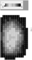
- FIG. 8 is a diagram of pressure test data of a chip in an existing chip packaging assembly.
- FIG. 9 is a diagram of pressure test data of a chip in a chip packaging assembly according to an embodiment of this application.
- a chip protected by a conductive gasket that serves as a cushion bears less pressure on the whole than a chip not protected by a conductive gasket.
- the chip packaging assembly may have better pressure bearing performance, to ensure structural stability of the chip packaging assembly during assembly, transportation, and the like.
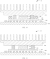
- an embodiment of this application provides another chip packaging assembly 12a, including a substrate 100, a chip 110, a seal ring 120, a heat sink 130, and a suppression ring 140.
- the heat sink 130 in this embodiment includes a heat sink body 132 and a ring-shaped support 134.
- the ring-shaped support 134 is located on a side of the heat sink body 132 and extends toward the substrate 100.
- the ring-shaped support 134 of the heat sink 130 extends to be spaced from the seal ring 120.
- the suppression ring 140 is disposed between the ring-shaped support 134 and the seal ring 120.
- the suppression ring 140 may also reduce or even eliminate a gap between the heat sink 130 and the seal ring 120 by disposing the suppression ring 140 between the ring-shaped support 134 and the seal ring 120. This can suppress an electromagnetic wave radiated by the chip 110, to reduce electromagnetic noise of the chip packaging assembly 12a.
- the chip packaging assembly 12a and a radio frequency circuit are not easy to interfere with each other, to ensure normal operation of the chip packaging assembly 12a and the radio frequency circuit.
- the suppression ring may alternatively be located between the heat sink body and the seal ring. This can also shield the electromagnetic wave radiated by the chip, to reduce the electromagnetic noise of the chip packaging assembly.
- the ring-shaped support 134 is located on an outer side of the seal ring 120, but is not limited thereto.
- an embodiment of this application provides another chip packaging assembly 12b. In comparison with the chip packaging assembly 12a, a ring-shaped support 134 of the chip packaging assembly 12b is located on an inner side of a seal ring 120.
- an embodiment of this application provides another chip packaging assembly 12c. In comparison with the chip packaging assembly 12a, a ring-shaped support 134 of the chip packaging assembly 12c is located on a side that is of a seal ring 120 and that is away from a substrate 100.
- structures of the chip packaging assemblies (12b and 12c) are similar to a structure of the chip packaging assembly 12a, and both can implement functions similar to those of the chip packaging assembly 12a, to suppress an electromagnetic wave radiated by a chip 110 and reduce electromagnetic noise of the chip packaging assemblies (12b and 12c). Details are not described herein again.
- a suppression ring 140 in this embodiment includes a first ring-shaped part 142 and a second ring-shaped part 144. Both the first ring-shaped part 142 and the second ring-shaped part 144 are ring-shaped. The first ring-shaped part 142 extends in an axial direction of the suppression ring 140. The second ring-shaped part 144 extends in a radial direction of the suppression ring 140. In this way, in the radial direction of the suppression ring 140, a cross section of the suppression ring 140 is substantially L-shaped.
- the first ring-shaped part 142 is disposed between a ring-shaped support 134 and a seal ring 120, and the second ring-shaped part 144 is disposed between a heat sink body 132 and the seal ring 120, to cooperate with each other to suppress an electromagnetic wave radiated by a chip 110. This can reduce electromagnetic noise of the chip packaging assembly and a possibility of crosstalk with a radio frequency circuit.
- the first ring-shaped part 142 may be, for example, a ring-shaped mechanical part made of a wave-absorbing material; or the first ring-shaped part 142 may be, for example, a conductive gasket.
- the second ring-shaped part 144 may be, for example, a conductive gasket. In this way, the second ring-shaped part 144 can further reduce pressure borne by the chip 110 while shielding the electromagnetic wave.
- first ring-shaped part 142 and the second ring-shaped part 144 may be an integrated ring-shaped mechanical part made of a wave-absorbing material; or the first ring-shaped part 142 and the second ring-shaped part 144 may be an integrated conductive gasket.
- an embodiment of this application provides yet another chip packaging assembly 14, including a substrate 100, a chip 110, a seal ring 120, a heat sink 130, and a suppression ring 140.
- the suppression ring 140 in this embodiment is directly disposed between the substrate 100 and the heat sink 130 through surrounding, and is located on an inner side of the seal ring 120.
- the substrate 100, the suppression ring 140, and the heat sink 130 jointly form an enclosed space.
- the chip 110 is located in the enclosed space.
- an electromagnetic wave radiated by the chip 110 is directly suppressed by the suppression ring 140 and the heat sink 130. Similar to the chip packaging assemblies (11a, 11b, 12a, 12b, 12c, and 13) in the foregoing embodiments, it is difficult for the electromagnetic wave radiated by the chip 110 to penetrate to outside of the chip packaging assembly 14. This can also reduce a possibility that the chip 110 externally radiates an electromagnetic wave, to reduce electromagnetic noise of the chip packaging assembly 14. In addition, the chip packaging assembly 14 and the radio frequency circuit are not easy to cross talk with each other.
- a size of the conductive gasket in this embodiment is larger than those of related structures (for example, the conductive gasket located between the seal ring 120 and the heat sink 130) in the foregoing embodiments.
- an elastic deformation range of the conductive gasket is relatively large. A skilled person can more conveniently control resilience of the conductive gasket, to improve compatibility of the conductive gasket and better protect the chip 110.
- a compression rate of the conductive gasket is controlled to be 30% to 40%. If a thickness of the conductive gasket between the seal ring 120 and the heat sink 130 is 2 mm, the elastic deformation range of the conductive gasket is 0.6 mm to 0.8 mm. If a thickness of the conductive gasket between the substrate 100 and the heat sink 130 is 6 mm, an elastic deformation range of the conductive gasket is 1.8 mm to 2.4 mm. Therefore, the conductive gasket with the thickness of 6 mm can have a larger adjustment range than the conductive gasket with the thickness of 2 mm.
- the skilled person can relatively conveniently adjust a distance between the heat sink 130 and the substrate 100, to adjust the compression rate of the conductive gasket and package the chip packaging assembly 14.
- an embodiment of this application provides still yet another chip packaging assembly 15, including a substrate 100, a chip 110, a heat sink 130, and a suppression ring 140.
- the chip packaging assembly 15 is not provided with the seal ring 120.
- the suppression ring 140 is disposed between the substrate 100 and the heat sink 130 through surrounding, to form an enclosed space together with the substrate 100 and the heat sink 130.
- an electromagnetic wave radiated by the chip 110 may also be suppressed through cooperation between the substrate 100, the heat sink 130, and the suppression ring 140, to reduce electromagnetic noise of the chip packaging assembly 15.
- the chip packaging assembly 15 and a radio frequency circuit are not easy to cross talk with each other.
Landscapes
- Shielding Devices Or Components To Electric Or Magnetic Fields (AREA)
- Cooling Or The Like Of Semiconductors Or Solid State Devices (AREA)
Applications Claiming Priority (2)
| Application Number | Priority Date | Filing Date | Title |
|---|---|---|---|
| CN202011161152.1A CN114496944B (zh) | 2020-10-26 | 2020-10-26 | 减小芯片电磁噪声的散热组件、芯片封装组件及电子设备 |
| PCT/CN2021/126125 WO2022089366A1 (zh) | 2020-10-26 | 2021-10-25 | 减小芯片电磁噪声的散热组件、芯片封装组件及电子设备 |
Publications (2)
| Publication Number | Publication Date |
|---|---|
| EP4220705A1 true EP4220705A1 (de) | 2023-08-02 |
| EP4220705A4 EP4220705A4 (de) | 2024-06-12 |
Family
ID=81383635
Family Applications (1)
| Application Number | Title | Priority Date | Filing Date |
|---|---|---|---|
| EP21885093.1A Pending EP4220705A4 (de) | 2020-10-26 | 2021-10-25 | Wärmeableitungsanordnung zur reduzierung von elektromagnetischem rauschen eines chips, chipgehäuseanordnung und elektronische vorrichtung |
Country Status (3)
| Country | Link |
|---|---|
| EP (1) | EP4220705A4 (de) |
| CN (2) | CN114496944B (de) |
| WO (1) | WO2022089366A1 (de) |
Cited By (1)
| Publication number | Priority date | Publication date | Assignee | Title |
|---|---|---|---|---|
| WO2026084794A1 (en) * | 2024-10-18 | 2026-04-23 | Qualcomm Incorporated | Frame configured to support cooling and shielding for an integrated circuit device |
Families Citing this family (1)
| Publication number | Priority date | Publication date | Assignee | Title |
|---|---|---|---|---|
| CN116207079A (zh) * | 2021-11-30 | 2023-06-02 | 华为技术有限公司 | 一种屏蔽结构、封装体、板级架构、散热器及电子设备 |
Family Cites Families (11)
| Publication number | Priority date | Publication date | Assignee | Title |
|---|---|---|---|---|
| US6044899A (en) * | 1998-04-27 | 2000-04-04 | Hewlett-Packard Company | Low EMI emissions heat sink device |
| US8213180B2 (en) * | 2010-01-21 | 2012-07-03 | Broadcom Corporation | Electromagnetic interference shield with integrated heat sink |
| US9048124B2 (en) * | 2012-09-20 | 2015-06-02 | Apple Inc. | Heat sinking and electromagnetic shielding structures |
| CN103354228A (zh) * | 2013-07-10 | 2013-10-16 | 三星半导体(中国)研究开发有限公司 | 半导体封装件及其制造方法 |
| JP6477421B2 (ja) * | 2015-10-29 | 2019-03-06 | 三菱電機株式会社 | 半導体装置 |
| US10098220B2 (en) * | 2015-12-24 | 2018-10-09 | Intel Corporation | Electronic device heat transfer system and related methods |
| US10763218B2 (en) * | 2016-03-24 | 2020-09-01 | Intel Corporation | Electrical devices and methods for forming electrical devices |
| CN107546197B (zh) * | 2016-06-24 | 2021-04-16 | 瑞昱半导体股份有限公司 | 电子装置及其散热及电磁屏蔽结构 |
| CN208798266U (zh) * | 2018-08-13 | 2019-04-26 | 深圳市腾顺电子材料有限公司 | 电路板及用电器 |
| CN209487497U (zh) * | 2019-04-01 | 2019-10-11 | 深圳市赛盛技术有限公司 | 一种芯片结构 |
| US11081450B2 (en) * | 2019-09-27 | 2021-08-03 | Intel Corporation | Radiation shield around a component on a substrate |
-
2020
- 2020-10-26 CN CN202011161152.1A patent/CN114496944B/zh active Active
-
2021
- 2021-10-25 EP EP21885093.1A patent/EP4220705A4/de active Pending
- 2021-10-25 WO PCT/CN2021/126125 patent/WO2022089366A1/zh not_active Ceased
- 2021-10-25 CN CN202180072418.1A patent/CN116325136A/zh active Pending
Cited By (1)
| Publication number | Priority date | Publication date | Assignee | Title |
|---|---|---|---|---|
| WO2026084794A1 (en) * | 2024-10-18 | 2026-04-23 | Qualcomm Incorporated | Frame configured to support cooling and shielding for an integrated circuit device |
Also Published As
| Publication number | Publication date |
|---|---|
| CN116325136A (zh) | 2023-06-23 |
| EP4220705A4 (de) | 2024-06-12 |
| CN114496944A (zh) | 2022-05-13 |
| WO2022089366A1 (zh) | 2022-05-05 |
| CN114496944B (zh) | 2026-01-06 |
Similar Documents
| Publication | Publication Date | Title |
|---|---|---|
| US6507101B1 (en) | Lossy RF shield for integrated circuits | |
| US9018039B2 (en) | Circuit module and method of producing circuit module | |
| EP1221739A2 (de) | Folie für elektronische Teile und Verfahren zu deren Herstellung | |
| US20240324093A1 (en) | Circuit board assembly and electronic device | |
| US20230290743A1 (en) | Reinforcement Structure and Electronic Device | |
| CN106559974A (zh) | 包括导电材料的热界面材料 | |
| JP2017224904A (ja) | ミリ波帯通信装置 | |
| WO2022089366A1 (zh) | 减小芯片电磁噪声的散热组件、芯片封装组件及电子设备 | |
| JP2022080991A (ja) | 電磁波吸収シート | |
| CN113363728A (zh) | 抑制电磁辐射的小型化超宽带超材料吸波体结构和应用 | |
| CN113286418A (zh) | 一种高性能电磁辐射抑制结构 | |
| EP4181194B1 (de) | Gehäusekörper und herstellungsverfahren dafür, anschluss und elektronische vorrichtung | |
| WO2023098503A1 (zh) | 一种屏蔽结构、封装体、板级架构、散热器及电子设备 | |
| CN113346239B (zh) | 电子设备及通信系统 | |
| US11369049B2 (en) | Electromagnetic shielding element, and transmission line assembly and electronic structure package using the same | |
| CN218071925U (zh) | 一种组合型散热屏蔽结构及电子组件 | |
| JP2010272585A (ja) | フリップチップ実装構造 | |
| US20100288553A1 (en) | Cooling pad capable of absorbing electromagnetic interference | |
| JP2018006586A (ja) | 電子制御装置 | |
| US10706832B2 (en) | Noise reduction device and printed circuit assembly including the same | |
| KR102123392B1 (ko) | 열전도성 emi 억제 조성 | |
| KR100651931B1 (ko) | 이동통신 단말기 | |
| US20250149473A1 (en) | Rf absorbing cover integrated in mmic packages | |
| CN218996711U (zh) | 一种散热屏蔽装置及电子设备 | |
| US20250300361A1 (en) | Electronic device and wave-absorbing structural component |
Legal Events
| Date | Code | Title | Description |
|---|---|---|---|
| STAA | Information on the status of an ep patent application or granted ep patent |
Free format text: STATUS: THE INTERNATIONAL PUBLICATION HAS BEEN MADE |
|
| PUAI | Public reference made under article 153(3) epc to a published international application that has entered the european phase |
Free format text: ORIGINAL CODE: 0009012 |
|
| STAA | Information on the status of an ep patent application or granted ep patent |
Free format text: STATUS: REQUEST FOR EXAMINATION WAS MADE |
|
| 17P | Request for examination filed |
Effective date: 20230427 |
|
| AK | Designated contracting states |
Kind code of ref document: A1 Designated state(s): AL AT BE BG CH CY CZ DE DK EE ES FI FR GB GR HR HU IE IS IT LI LT LU LV MC MK MT NL NO PL PT RO RS SE SI SK SM TR |
|
| DAV | Request for validation of the european patent (deleted) | ||
| DAX | Request for extension of the european patent (deleted) | ||
| REG | Reference to a national code |
Ref country code: DE Ref legal event code: R079 Free format text: PREVIOUS MAIN CLASS: H01L0023360000 Ipc: H01L0023552000 |
|
| RIC1 | Information provided on ipc code assigned before grant |
Ipc: H01L 23/367 20060101ALN20240213BHEP Ipc: H01L 23/16 20060101ALI20240213BHEP Ipc: H05K 9/00 20060101ALI20240213BHEP Ipc: H01L 23/10 20060101ALI20240213BHEP Ipc: H01L 23/552 20060101AFI20240213BHEP |
|
| A4 | Supplementary search report drawn up and despatched |
Effective date: 20240513 |
|
| RIC1 | Information provided on ipc code assigned before grant |
Ipc: H01L 23/367 20060101ALN20240506BHEP Ipc: H01L 23/16 20060101ALI20240506BHEP Ipc: H05K 9/00 20060101ALI20240506BHEP Ipc: H01L 23/10 20060101ALI20240506BHEP Ipc: H01L 23/552 20060101AFI20240506BHEP |