EP4220706A1 - Anordnung für eine halbleiteranordnung mit mindestens einem passiven bauelement und einem substrat - Google Patents
Anordnung für eine halbleiteranordnung mit mindestens einem passiven bauelement und einem substrat Download PDFInfo
- Publication number
- EP4220706A1 EP4220706A1 EP22154511.4A EP22154511A EP4220706A1 EP 4220706 A1 EP4220706 A1 EP 4220706A1 EP 22154511 A EP22154511 A EP 22154511A EP 4220706 A1 EP4220706 A1 EP 4220706A1
- Authority
- EP
- European Patent Office
- Prior art keywords
- metallization
- passive component
- arrangement
- dielectric material
- material layer
- Prior art date
- Legal status (The legal status is an assumption and is not a legal conclusion. Google has not performed a legal analysis and makes no representation as to the accuracy of the status listed.)
- Withdrawn
Links
Images





Classifications
-
- H—ELECTRICITY
- H10—SEMICONDUCTOR DEVICES; ELECTRIC SOLID-STATE DEVICES NOT OTHERWISE PROVIDED FOR
- H10W—GENERIC PACKAGES, INTERCONNECTIONS, CONNECTORS OR OTHER CONSTRUCTIONAL DETAILS OF DEVICES COVERED BY CLASS H10
- H10W40/00—Arrangements for thermal protection or thermal control
-
- H—ELECTRICITY
- H10—SEMICONDUCTOR DEVICES; ELECTRIC SOLID-STATE DEVICES NOT OTHERWISE PROVIDED FOR
- H10W—GENERIC PACKAGES, INTERCONNECTIONS, CONNECTORS OR OTHER CONSTRUCTIONAL DETAILS OF DEVICES COVERED BY CLASS H10
- H10W70/00—Package substrates; Interposers; Redistribution layers [RDL]
- H10W70/60—Insulating or insulated package substrates; Interposers; Redistribution layers
- H10W70/62—Insulating or insulated package substrates; Interposers; Redistribution layers characterised by their interconnections
- H10W70/65—Shapes or dispositions of interconnections
- H10W70/658—Shapes or dispositions of interconnections for devices provided for in groups H10D8/00 - H10D48/00
-
- H—ELECTRICITY
- H05—ELECTRIC TECHNIQUES NOT OTHERWISE PROVIDED FOR
- H05K—PRINTED CIRCUITS; CASINGS OR CONSTRUCTIONAL DETAILS OF ELECTRIC APPARATUS; MANUFACTURE OF ASSEMBLAGES OF ELECTRICAL COMPONENTS
- H05K1/00—Printed circuits
- H05K1/02—Details
- H05K1/03—Use of materials for the substrate
- H05K1/05—Insulated conductive substrates, e.g. insulated metal substrate
- H05K1/053—Insulated conductive substrates, e.g. insulated metal substrate the metal substrate being covered by an inorganic insulating layer
-
- H—ELECTRICITY
- H10—SEMICONDUCTOR DEVICES; ELECTRIC SOLID-STATE DEVICES NOT OTHERWISE PROVIDED FOR
- H10W—GENERIC PACKAGES, INTERCONNECTIONS, CONNECTORS OR OTHER CONSTRUCTIONAL DETAILS OF DEVICES COVERED BY CLASS H10
- H10W40/00—Arrangements for thermal protection or thermal control
- H10W40/20—Arrangements for cooling
- H10W40/25—Arrangements for cooling characterised by their materials
- H10W40/255—Arrangements for cooling characterised by their materials having a laminate or multilayered structure, e.g. direct bond copper [DBC] ceramic substrates
-
- H—ELECTRICITY
- H05—ELECTRIC TECHNIQUES NOT OTHERWISE PROVIDED FOR
- H05K—PRINTED CIRCUITS; CASINGS OR CONSTRUCTIONAL DETAILS OF ELECTRIC APPARATUS; MANUFACTURE OF ASSEMBLAGES OF ELECTRICAL COMPONENTS
- H05K1/00—Printed circuits
- H05K1/02—Details
- H05K1/03—Use of materials for the substrate
- H05K1/0306—Inorganic insulating substrates, e.g. ceramic, glass
-
- H—ELECTRICITY
- H05—ELECTRIC TECHNIQUES NOT OTHERWISE PROVIDED FOR
- H05K—PRINTED CIRCUITS; CASINGS OR CONSTRUCTIONAL DETAILS OF ELECTRIC APPARATUS; MANUFACTURE OF ASSEMBLAGES OF ELECTRICAL COMPONENTS
- H05K2201/00—Indexing scheme relating to printed circuits covered by H05K1/00
- H05K2201/09—Shape and layout
- H05K2201/09209—Shape and layout details of conductors
- H05K2201/09654—Shape and layout details of conductors covering at least two types of conductors provided for in H05K2201/09218 - H05K2201/095
- H05K2201/098—Special shape of the cross-section of conductors, e.g. very thick plated conductors
-
- H—ELECTRICITY
- H05—ELECTRIC TECHNIQUES NOT OTHERWISE PROVIDED FOR
- H05K—PRINTED CIRCUITS; CASINGS OR CONSTRUCTIONAL DETAILS OF ELECTRIC APPARATUS; MANUFACTURE OF ASSEMBLAGES OF ELECTRICAL COMPONENTS
- H05K2201/00—Indexing scheme relating to printed circuits covered by H05K1/00
- H05K2201/10—Details of components or other objects attached to or integrated in a printed circuit board
- H05K2201/10007—Types of components
- H05K2201/10022—Non-printed resistor
-
- H—ELECTRICITY
- H05—ELECTRIC TECHNIQUES NOT OTHERWISE PROVIDED FOR
- H05K—PRINTED CIRCUITS; CASINGS OR CONSTRUCTIONAL DETAILS OF ELECTRIC APPARATUS; MANUFACTURE OF ASSEMBLAGES OF ELECTRICAL COMPONENTS
- H05K2201/00—Indexing scheme relating to printed circuits covered by H05K1/00
- H05K2201/10—Details of components or other objects attached to or integrated in a printed circuit board
- H05K2201/10007—Types of components
- H05K2201/10166—Transistor
-
- H—ELECTRICITY
- H05—ELECTRIC TECHNIQUES NOT OTHERWISE PROVIDED FOR
- H05K—PRINTED CIRCUITS; CASINGS OR CONSTRUCTIONAL DETAILS OF ELECTRIC APPARATUS; MANUFACTURE OF ASSEMBLAGES OF ELECTRICAL COMPONENTS
- H05K3/00—Apparatus or processes for manufacturing printed circuits
- H05K3/30—Assembling printed circuits with electric components, e.g. with resistors
- H05K3/32—Assembling printed circuits with electric components, e.g. with resistors electrically connecting electric components or wires to printed circuits
- H05K3/34—Assembling printed circuits with electric components, e.g. with resistors electrically connecting electric components or wires to printed circuits by soldering
- H05K3/3465—Application of solder
- H05K3/3478—Application of solder preforms; Transferring prefabricated solder patterns
-
- H—ELECTRICITY
- H10—SEMICONDUCTOR DEVICES; ELECTRIC SOLID-STATE DEVICES NOT OTHERWISE PROVIDED FOR
- H10W—GENERIC PACKAGES, INTERCONNECTIONS, CONNECTORS OR OTHER CONSTRUCTIONAL DETAILS OF DEVICES COVERED BY CLASS H10
- H10W90/00—Package configurations
- H10W90/401—Package configurations characterised by multiple insulating or insulated package substrates, interposers or RDLs
-
- H—ELECTRICITY
- H10—SEMICONDUCTOR DEVICES; ELECTRIC SOLID-STATE DEVICES NOT OTHERWISE PROVIDED FOR
- H10W—GENERIC PACKAGES, INTERCONNECTIONS, CONNECTORS OR OTHER CONSTRUCTIONAL DETAILS OF DEVICES COVERED BY CLASS H10
- H10W90/00—Package configurations
- H10W90/701—Package configurations characterised by the relative positions of pads or connectors relative to package parts
Definitions
- the invention relates to an arrangement for a semiconductor arrangement with at least one passive component and a substrate, the substrate having a dielectric material layer and a first metallization arranged on the dielectric material layer.
- the invention relates to a semiconductor arrangement, in particular a planar semiconductor arrangement, having at least one such arrangement.
- the invention relates to a power converter with at least one semiconductor arrangement.
- the invention relates to a method for producing an arrangement for a semiconductor arrangement having at least one passive component and a substrate, the substrate having a dielectric material layer and a first metallization arranged on the dielectric material layer.
- a power converter is to be understood, for example, as a rectifier, an inverter, a converter or a DC voltage converter.
- components such as capacitors, snubbers, but also sensors, among other things for determining currents, voltages or temperatures, can be used, which are usually soldered onto a substrate.
- sensors can include, for example, a current measuring resistor, a so-called shunt resistor, or a negative temperature coefficient thermistor, NTC for short.
- the components can be placed partially in a current-carrying path or in the area of a heat source, for example in order to achieve accurate measurement results be arranged, whereby sufficient heat dissipation is to be ensured.
- the installation space and the service life pose a major challenge.
- EP 3 625 823 A1 describes a power module with at least one power semiconductor, in particular a power transistor, which has a first contact area and a second contact area opposite the first contact area, and a substrate which comprises at least two layers arranged one above the other and connected to one another.
- the first layer comprises a first dielectric material with at least one first metallization
- the first metallization is arranged on a side facing the second layer
- the second layer comprising a second dielectric material with at least one second metallization
- the second metallization being arranged on a side facing away from the first metallization
- the power semiconductor being connected to the first metallization via the first contact area is connected
- the power semiconductor being arranged in a first cutout of the second layer
- a metallic first encapsulation being arranged in such a way that the power semiconductor is encapsulated in a fluid-tight manner and the second contact area of the power semiconductor is electrically conductively connected to the second metallization via the first encapsulation.
- the disclosure document WO 2020/249479 A1 describes an electronic circuit with a first and a second circuit carrier and a first and a second semiconductor component.
- the first semiconductor component rests with an upper side on an underside of the first circuit carrier and with an underside on an upper side of the second circuit carrier.
- the first circuit carrier has a first via, which connects the first semiconductor component to a first conductor track.
- the first circuit carrier has a second via, which electrically connects a connecting element arranged between the circuit carriers to a further conductor track.
- this object is achieved in that the passive component is arranged completely in a recess in the first metallization and rests directly on the dielectric material layer.
- the object is achieved according to the invention by a semiconductor arrangement, in particular a planar semiconductor arrangement, with at least one such arrangement.
- the object is achieved according to the invention by a power converter with at least one semiconductor arrangement.
- the object is achieved in a method of the type mentioned in that the passive component is arranged completely and in such a way in a recess of the first metallization that the passive component rests directly on the dielectric material layer.
- the invention is based on the idea of reducing the installation space of at least one passive component in an arrangement for a semiconductor arrangement by fitting it completely in a recess in a first metallization of a Substrate is arranged.
- a recess is a continuous recess in the first metallization.
- This continuous recess can have, among other things, a rectangular outer contour.
- a semiconductor arrangement can be, inter alia, a power semiconductor module.
- Such a passive component, in particular at least partially metallic can be designed, among other things, as a resistance sensor, in particular as a shunt resistor or as an NTC.
- such a resistance sensor is at least partially made of an alloy which can contain, among other things, Zeranin, Manganin, Constantan, Isaohm or a PTC thermistor such as platinum.
- the first metallization of the substrate can contain copper, silver or gold, for example.
- the dielectric material layer can contain, among other things, a ceramic material, for example aluminum nitride or aluminum oxide, or an organic material, for example a polyamide or epoxy resin.
- the passive component which is essentially cuboid, for example, is connected to the dielectric material layer over its entire surface. Such a connection saves installation space in addition to improved heat dissipation, since, among other things, further components can be placed closer to the passive component. Furthermore, the integration of the at least one passive component simplifies the manufacturing process, since an assembly process and soldering are no longer necessary.
- a further embodiment provides that the passive component is flush with a first surface of the first metallization completes. Such a flush termination makes it easier for the first metallization to be pressed on with the passive component, so that the passive component can be reliably contacted with the dielectric material layer over its entire surface.
- a further embodiment provides that the first metallization is designed as a thick copper substrate, the passive component being pressed with the dielectric material layer over the entire surface between two sides of the thick copper substrate.
- a thick copper substrate has a copper thickness of at least 1 mm. Such a connection is robust and easy to produce.
- a further embodiment provides that the passive component is connected directly or via connecting means in the recess of the first metallization.
- a direct connection can be produced, for example, by direct pressing or by a shrink connection.
- a press-fit connection is produced, for example, via which the passive component is connected to the first metallization.
- Such non-positive connections are robust and easy to produce.
- a further embodiment provides that the passive component is made from a first material, with the connecting means containing a second material which differs from the first material at least with regard to its mechanical and/or thermal properties.
- Connecting means can be, for example, tin flakes or a coating of the passive component, which contains, for example, copper-tin (Cu-Sn), copper-nickel-silicon (Cu-Ni-Si) or copper-chromium-silver (Cu-Cr-Ag).
- Thermal stresses that occur during operation for example, are reduced by different mechanical and/or thermal properties, such as coefficients of expansion and/or modulus of elasticity.
- use the lanyard a material connection between the passive component and the first metallization can be produced. For example, a small piece of tin is melted to produce a material connection. By reducing stresses, particularly thermal stresses, such connections contribute to extending the service life of the arrangement.
- a further embodiment provides that the passive component has a first profiling and the first metallization has a second profiling in the area of contact with the passive component, with the profilings engaging with one another.
- the first metallization has a recess, in particular a fold and/or a chamfer, which engages with an at least partially corresponding overhang of the passive component, as a result of which a form fit is formed. Such a form fit increases the reliability of the connection.
- a further embodiment provides that the passive component is connected to the dielectric material layer via a force acting through the form-fitting connection perpendicularly to the first surface. Such a connection reduces stresses acting on the passive component.
- a further embodiment provides that the substrate has a second metallization, which is designed as a thick copper substrate, the dielectric material layer being laminated onto the second metallization or pressed with the second metallization, the second metallization being connected to the first metallization via the dielectric material layer is.
- a production method of this type makes it possible to produce a very thin substrate layer, which improves heat dissipation via the second metallization.
- the passive component is designed as a sensor and the arrangement comprises at least one connection for contacting the sensor.
- the sensor is designed as a shunt resistor containing Zeranin, Manganin, Konstantan, Isaohm. An integration of such a shunt resistor improves the thermal connection, so that high measurement accuracy and a long service life can be achieved.
- the sensor can be designed as a temperature sensor, e.g. as an NTC, which contains a PTC thermistor, in particular platinum. Accurate temperature measurement is made possible by improving the thermal connection to the environment via the substrate.
- the described components of the embodiments each represent individual features of the invention to be considered independently of one another, which also develop the invention independently of one another and are therefore also to be regarded as part of the invention individually or in a combination other than the one shown. Furthermore, the described embodiments can also be supplemented by other features of the invention already described.
- FIG 1 shows a schematic cross-sectional view of a first embodiment of an arrangement 2 with a passive component 4 and a substrate 6.
- the substrate 6 comprises a dielectric material layer 8, which is arranged between a first metallization 10 and a second metallization 12, the first metallization 10 on the dielectric material layer 8 is connected to the second metallization 12 in an electrically insulating and thermally conductive manner.
- the dielectric material layer 8 can contain, among other things, a ceramic material, for example aluminum nitride or aluminum oxide, an organic material, for example a polyamide, or an organic material filled with a ceramic material.
- the first metallization 10 and the second metallization 12 are embodied as a thick copper substrate with a thickness s of at least 1 mm.
- the first metallization 10 has a recess 14 in which the passive component 4 is arranged.
- the passive component 4 is arranged completely in the cutout 14, that is to say it does not protrude beyond the cutout 14.
- The, in particular metallic, passive component 4 can be designed, among other things, as a resistance sensor, in particular as a shunt resistor or as an NTC.
- a resistance sensor is made from an alloy which can contain, among other things, Zeranin, Manganin, Constantan, Isaohm or a PTC thermistor such as platinum.
- the recess 14 of the first metallization 10 is designed as a continuous recess up to the dielectric material layer 8 .
- the passive component 4, which in FIG 1 is designed essentially cuboid, is directly, that is, without further connecting means, between a first Side 16 and a second side 18 of the thick copper substrate connected.
- the passive component 4 is non-positively connected to the thick copper substrate, in particular by direct pressing or by a shrinkage connection.
- the passive component 4 connected to the thick copper substrate is pressed onto the dielectric material layer 8 over its entire surface, with the passive component 4 resting directly over its entire surface on the dielectric material layer 8 and thus being connected to the second metallization 12 in an electrically insulating and thermally conductive manner.
- the passive component 4 can be dissipated via the dielectric material layer 8 .
- a good thermal connection to neighboring components, such as a power semiconductor component can be established.
- the passive component 4 terminates at a distance a, which is in the pm range, for example, below a first surface 20 of the first metallization 10, with the first surface 20 of the first metallization 10 defining a horizontal plane. The passive component 4 is therefore integrated into the substrate 6 so that space is saved in the vertical direction.
- FIG 2 shows a schematic cross-sectional representation of a second embodiment of an arrangement 2 with a passive component 4 and a substrate 6, wherein the passive component 4 arranged in the cutout 14 of the first metallization 10, in particular non-positively connected, terminates flush with the first surface 20 of the first metallization 10 .
- the passive component 4 is integrated into the substrate 6, with installation space being saved in the vertical direction. Furthermore, the flush termination makes it easier to press the first metallization 10 onto the passive component 4, so that the passive component 4 can be reliably contacted with the dielectric material layer 8 over the entire surface.
- the further execution of the arrangement 2 in FIG 2 corresponds to the in FIG 1 .
- the passive component 4 comprises a metallic layer 4a and a dielectric layer 4b arranged on a side of the metallic layer 4a facing the dielectric material layer 8.
- the dielectric layer 4b is designed to be electrically insulating and can contain, among other things, an organic material, in particular a plastic, or a ceramic material.
- a thermally conductive connection of the metallic layer 4a of the passive component 4 to the dielectric material layer 8 is made possible by the dielectric layer 4b.
- a resistance value of the passive component 4 terminating flush with the first surface 20 of the first metallization 10 can be flexibly adjusted, among other things, by varying a thickness d of the metallic layer 4a.
- the further execution of the arrangement 2 in 3 corresponds to the in FIG 2 .
- FIG 4 shows a schematic cross-sectional illustration of a fourth embodiment of an arrangement 2 with a passive component 4 and a substrate 6, the passive component 4 being connected on both sides via connecting means 22 in the recess 14 of the first metallization 10.
- the connecting means 22 are tin plates, for example.
- the connecting means 22 can be a coating, in particular of the passive component 4, which, for example, has copper-tin (Cu-Sn), copper-nickel-silicon (Cu-Ni-Si) or copper-chromium-silver (Cu-Cr- Ag) contains.
- a press-fit connection is produced by means of the connecting means 22, via which the passive component 4 is connected to the first metallization 10.
- Thermal stresses that occur during operation are reduced by different mechanical and/or thermal properties, such as coefficients of expansion and/or modulus of elasticity.
- a material connection between the passive component 4 and the first metallization 10 is produced via the connecting means 22 .
- the other Execution of the arrangement 2 in FIG 4 corresponds to the in 3 .
- FIG. 5 shows a schematic cross-sectional representation of a fifth embodiment of an arrangement 2 with a passive component 4 and a substrate 6, the passive component 4 having a first profile 24 on each side and the first metallization 10 in the region of contact with the passive component 4 each having a second profile 26 having.
- the first metallization 10 has a recess in the form of a fold, with the passive component 4 having a projection which engages with the recess of the first metallization 10 .
- a form-fitting connection is formed by the profiles 22, 24 which are in engagement with one another. Additionally or alternatively, the profiles 22, 24 each have a chamfer.
- connecting means 22 are arranged in each case, which connect the passive component 4 to the first metallization 10 .
- the arrangement 2 has compensating structures 28 for compensating for, in particular thermally induced, expansions.
- the passive component 4 is thus connected to the dielectric material layer 8 via a force F acting perpendicularly to the first surface 20 as a result of the form-fitting connection.
- the further execution of the arrangement 2 in 5 corresponds to the in FIG 4 .
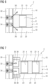
- FIG. 6 shows a schematic representation of a section of a sixth embodiment of an arrangement 2 with a passive component 4 and a substrate 6 in a plan view.
- the arrangement 2 is arranged in a housing 30 and includes terminals 32, 34 for contacting the passive component 4.
- the terminals 32, 34 are embodied as housing pins, which are connected via bonding connection means 36, in particular bonding wires, to one side 16, 18 of the first Metallization 10 are connected.
- the passive component 4 is contacted by the terminals 32, 34 in such a way that, for example, determining a voltage drop across the passive component 4 or a current flowing through the passive component 4 is made possible.
- the passive component 4 is designed as an NTC resistor for use as a temperature sensor, the NTC resistor containing platinum.
- the further execution of the arrangement 2 in 6 corresponds to the in FIG 4 .
- FIG 7 shows a schematic representation of a section of a seventh embodiment of an arrangement with a passive component and a substrate in a plan view, two passive components 4 being connected in parallel, for example.
- the passive components 4 are designed, for example, as shunt resistors for measuring a load current in a power semiconductor module and are made from an alloy containing Zeranin, Manganin, Constantan or Isaohm.
- the first metallization 10 has a contact pad 38 on both sides 16, 18 for contacting the connections 32, 34.
- the connections 32, 34 are connected to the contact pads 38 via bonding connection means 36, in particular bonding wires. Via the terminals 32, 34, it is possible to determine a voltage drop across the passive components 4, in particular to determine a current.
- the further execution of the arrangement 2 in FIG 7 corresponds to the in 6 .
- a dielectric material layer 8 is laminated onto a second metallization 12, which is designed as a thick copper substrate. Alternatively, the dielectric material layer 8 is connected to the second metallization 12 by pressing.
- a passive component 4 is introduced in this way into a cavity 44 of a first metallization 10 designed as a thick copper substrate and between two sides 16, 18 of the first metallization 10 to form a top layer 40 connected.
- the top layer 40 is pressed with the dielectric material layer 8 using a pressing device 42, for example a press die, in particular a flat one, in such a way that the passive component 4 rests over the entire surface and directly on the dielectric material layer 8 and is flush with a first surface 20 of the first Metallization 10 completes.
- the connection of the passive component 4 to the first metallization 10 and the pressing with the dielectric material layer 8 by the pressing device 42 can take place simultaneously.
- the steps shown can be carried out in one pressing operation, particularly if the dielectric can only be cured once.
- the further execution of the arrangement 2 in 8 corresponds to the in FIG 2 .
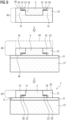
- FIG. 9 shows a schematic representation of a second method for producing an arrangement 2 with a passive component 4 and a substrate 6, the passive component 4 being introduced into a cavity 44 of the first metallization 10 designed as a thick copper substrate and with the first metallization 10 to form a top layer 40 is connected.
- the cavity 44 of the first metallization 10 has a recess in the form of a fold on both sides 16, 18, with the passive component 4 having a projection which engages with the recess of the first metallization 10.
- the passive component 4 is connected in the region of its overhangs arranged on both sides via connecting means 22, in particular small tin plates, to the first metallization 10 and the arrangement 2 has compensating structures 28 for compensating for, in particular thermally induced, expansions.
- the compensating structures 28 are filled with a filling material, for example with silicone, in order to prevent partial discharges.
- the passive component 4 ends flush with a second surface 46 of the first metallization 10 .
- the top layer 40 is such over the second surface 46 with the dielectric material layer 8 pressed so that the passive component 4 rests directly on the dielectric material layer 8 .
- a layer 48 of the first metallization 10 arranged on a side facing away from the passive component 4 is removed by machining, eg by milling, in such a way that the cavity 44 becomes a recess 14 in the first metallization 10 . Furthermore, the removal of the layer 48 exposes the passive component 4 , the passive component 4 terminating flush with the first surface 20 of the first metallization 10 .
- the further execution of the arrangement 2 in 9 corresponds to the in 5 .
- FIG. 10 shows a schematic representation of a third method for producing an arrangement 2 with a passive component 4 and a substrate 6, the passive component 4 being introduced into a cavity 44 of the first metallization 10 designed as a thick copper substrate and with the first metallization 10 to form a top layer 40 is connected.
- the passive component 4 is non-positively connected to the thick copper substrate, in particular by direct pressing or by a shrinkage connection.
- the passive component 4 ends flush with the first surface 20 of the first metallization 10 .
- a layer 48 of the first metallization 10 arranged on a side facing away from the passive component 4 is removed, in particular by means of machining, in such a way that the passive component 4 is exposed and the passive component 4 is flush with a second surface 46 of the first Metallization 10 completes.
- the remaining part of the top layer 40 is pressed over the second surface 46 with the dielectric material layer 8 in such a way that the passive component 4 is directly on the dielectric material layer 8 rests.
- the further execution of the arrangement 2 in 9 corresponds to the in 5 .
- FIG. 1 shows a schematic cross-sectional view of a semiconductor arrangement 50, which includes a semiconductor component 52 that is implemented using planar assembly and connection technology.
- the semiconductor component 52 is embodied as a vertical power transistor, in particular as an insulated gate bipolar transistor (IGBT).
- the power transistor is connected to a printed circuit board 54, in particular a printed circuit board (PCB), via a first power connection 52a.
- the power transistor is connected to a substrate 6, which is embodied as a DCB substrate, via a second power connection 52b and a control connection 52c.
- the second power connection 52b and the control connection 52c are electrically conductively connected to the printed circuit board 54 via spacer elements 56, also known as changeovers.
- the semiconductor arrangement 50 has an arrangement 2 with a passive component 4, which can be designed according to one of the previous figures.
- the passive component 4 is configured to sense a current of the second power terminal 52b.
- the substrate 6 is also connected to a heat sink 58, for example a heat sink, so that the semiconductor component 52 and the passive component 4 are connected to the heat sink 58 in an electrically insulating and thermally conductive manner.
- a potting material 60 is arranged between the circuit board 54 and the substrate 6, in which the semiconductor component 52, the spacer elements 56 and the passive component 4 are embedded.
- the encapsulation material 60 is produced with the aid of an underfill, for example.
- FIG. 12 1 shows a schematic representation of a power converter which, by way of example, comprises a semiconductor arrangement 50 with an arrangement 2 .
- the invention relates to an arrangement 2 for a semiconductor arrangement 50 with at least one passive component 4 and a substrate 6 , the substrate 6 having a dielectric material layer 8 and a first metallization 10 arranged on the dielectric material layer 8 .
- the passive component 4 be arranged completely in a cutout 14 of the first metallization 10 and lie directly on the dielectric material layer 8 .
Landscapes
- Chemical & Material Sciences (AREA)
- Inorganic Chemistry (AREA)
- Engineering & Computer Science (AREA)
- Microelectronics & Electronic Packaging (AREA)
- Cooling Or The Like Of Semiconductors Or Solid State Devices (AREA)
- Structures For Mounting Electric Components On Printed Circuit Boards (AREA)
- Structure Of Printed Boards (AREA)
Abstract
Die Erfindung betrifft eine Anordnung (2) für eine Halbleiteranordnung (50) mit mindestens einem passiven Bauelement (4) und einem Substrat (6), wobei das Substrat (6) eine dielektrische Materiallage (8) und eine auf der dielektrische Materiallage (8) angeordnete erste Metallisierung (10) aufweist. Um den Bauraum der Anordnung (2) zu verringern und eine verbesserte Entwärmung zu ermöglichen, wird vorgeschlagen, dass das passive Bauelement (4) vollständig in einer Aussparung (14) der ersten Metallisierung (10) angeordnet ist und unmittelbar auf der dielektrischen Materiallage (8) aufliegt.
Description
- Die Erfindung betrifft eine Anordnung für eine Halbleiteranordnung mit mindestens einem passiven Bauelement und einem Substrat, wobei das Substrat eine dielektrische Materiallage und eine auf der dielektrische Materiallage angeordnete erste Metallisierung aufweist.
- Ferner betrifft die Erfindung eine Halbleiteranordnung, insbesondere eine planare Halbleiteranordnung, mit mindestens einer derartigen Anordnung.
- Überdies betrifft die Erfindung einen Stromrichter mit mindestens einer Halbleiteranordnung.
- Darüber hinaus betrifft die Erfindung ein Verfahren zur Herstellung einer Anordnung für eine Halbleiteranordnung mit mindestens einem passiven Bauelement und einem Substrat, wobei das Substrat eine dielektrische Materiallage und eine auf der dielektrischen Materiallage angeordnete erste Metallisierung aufweist.
- Derartige Anordnungen kommen beispielsweise in einem Stromrichter zum Einsatz. Unter einem Stromrichter ist beispielsweise ein Gleichrichter, ein Wechselrichter, ein Umrichter oder ein Gleichspannungswandler zu verstehen. In einem Stromrichter können Bauelemente wie Kondensatoren, Snubber aber auch Sensoren, unter anderem zur Ermittlung von Strömen, Spannungen oder Temperaturen, zum Einsatz kommen, die üblicherweise auf einem Substrat aufgelötet sind. Derartige Sensoren können beispielsweise einen Strommesswiderstand, einen sogenannten Shunt-Widerstand oder einen Negative Temperature Coefficient Thermistor, kurz NTC, umfassen. Die Bauteile können teilweise, z.B. um genaue Messergebnisse zu erzielen, in einen stromführenden Pfad oder im Bereich einer Wärmequelle angeordnet werden, wobei eine ausreichende Entwärmung zu gewährleisten ist. Ferner stellen mit zunehmender Miniaturisierung der Bauraum und die Lebensdauer eine große Herausforderung dar.
- Die Offenlegungsschrift
EP 3 625 823 A1 beschreibt ein Leistungsmodul mit mindestens einem Leistungshalbleiter, insbesondere einem Leistungstransistor, welcher eine erste Kontaktfläche und eine der ersten Kontaktfläche gegenüberliegende zweite Kontaktfläche aufweist, und einem Substrat, welches zumindest zwei übereinander angeordnete miteinander verbundene Lagen umfasst. Um eine, im Vergleich zum Stand der Technik, höhere Beständigkeit gegenüber Feuchtigkeit zu erreichen und eine niederinduktive planare Anbindung des mindestens einen Leistungshalbleiters zu ermöglichen, wird vorgeschlagen, dass die erste Lage ein erstes dielektrisches Material mit zumindest einer ersten Metallisierung umfasst, wobei die erste Metallisierung auf einer der zweiten Lage zugewandten Seite angeordnet ist, wobei die zweite Lage ein zweites dielektrisches Material mit zumindest einer zweiten Metallisierung umfasst, wobei die zweite Metallisierung auf einer der ersten Metallisierung abgewandten Seite angeordnet ist, wobei der Leistungshalbleiter über die erste Kontaktfläche mit der ersten Metallisierung verbunden ist, wobei der Leistungshalbleiter in einer ersten Aussparung der zweiten Lage angeordnet ist, wobei eine metallische erste Kapselung derartig angeordnet ist, dass der Leistungshalbleiter fluiddicht gekapselt ist und die zweite Kontaktfläche des Leistungshalbleiters über die erste Kapselung elektrisch leitend mit der zweiten Metallisierung verbunden ist. - Die Offenlegungsschrift
WO 2020/249479 A1 beschreibt einen elektronischen Schaltkreis mit einem ersten und einem zweiten Schaltungsträger sowie einem ersten und einem zweiten Halbleiterbauelement. Das erste Halbleiterbauelement liegt mit einer Oberseite an einer Unterseite des ersten Schaltungsträgers an sowie mit einer Unterseite an einer Oberseite des zweiten Schaltungsträgers. Der erste Schaltungsträger weist eine erste Durchkontaktierung auf, welche das erste Halbleiterbauelement mit einer ersten Leiterbahn verbindet. Der erste Schaltungsträger weist eine zweite Durchkontaktierung auf, welche ein zwischen den Schaltungsträgern angeordnetes Verbindungselement mit einer weiteren Leiterbahn elektrisch verbindet. - Vor diesem Hintergrund ist es eine Aufgabe der vorliegenden Erfindung, den Bauraum einer derartigen Anordnung zu verringern und eine verbesserte Entwärmung zu ermöglichen.
- Diese Aufgabe wird bei einer Anordnung eingangs genannter Art dadurch gelöst, dass das passive Bauelement vollständig in einer Aussparung der ersten Metallisierung angeordnet ist und unmittelbar auf der dielektrischen Materiallage aufliegt.
- Ferner wird die Aufgabe erfindungsgemäß gelöst durch eine Halbleiteranordnung, insbesondere eine planare Halbleiteranordnung, mit mindestens einer derartigen Anordnung.
- Überdies wird die Aufgabe erfindungsgemäß gelöst durch einen Stromrichter mit mindestens einer Halbleiteranordnung.
- Darüber hinaus wird die Aufgabe bei einem Verfahren eingangs genannter Art dadurch gelöst, dass das passive Bauelement vollständig und derartig in einer Aussparung der ersten Metallisierung angeordnet wird, dass das passive Bauelement unmittelbar auf der dielektrischen Materiallage aufliegt.
- Die in Bezug auf die Anordnung nachstehend angeführten Vorteile und bevorzugten Ausgestaltungen lassen sich sinngemäß auf die Halbleiteranordnung, den Stromrichter und das Verfahren übertragen.
- Der Erfindung liegt die Überlegung zugrunde, den Bauraum mindestens eines passiven Bauelements in einer Anordnung für eine Halbleiteranordnung zu verringern, indem dieses vollständig in einer Aussparung einer ersten Metallisierung eines Substrats angeordnet wird. Eine Aussparung ist in diesem Zusammenhang eine durchgängige Ausnehmung der ersten Metallisierung. Diese durchgängige Ausnehmung kann unter anderem eine rechteckige Außenkontur aufweisen. Eine Halbleiteranordnung kann unter anderem ein Leistungshalbleitermodul sein. Ein derartiges, insbesondere zumindest teilweise metallisches, passives Bauelement kann unter anderem als Widerstandssensor, insbesondere als Shunt-Widerstand oder als NTC ausgeführt sein. Beispielsweise ist ein derartiger Widerstandssensor zumindest teilweise aus einer Legierung hergestellt, welche unter anderem Zeranin, Manganin, Konstantan, Isaohm oder einen Kaltleiter wie Platin enthalten kann. Die erste Metallisierung des Substrats kann beispielsweise Kupfer, Silber oder Gold enthalten. Durch eine derartige Integration des passiven Bauelements in die erste Metallisierung wird Bauraum, insbesondere in vertikale Richtung, eingespart.
- Um eine ausreichende thermische Anbindung und damit eine effiziente Entwärmung des mindestens einen passiven Bauelements zu ermöglichen, liegt dieses unmittelbar, das heißt ohne weitere Verbindungsmittel, auf der dielektrischen Materiallage des Substrats auf. Die dielektrische Materiallage kann unter anderem einen keramischen Werkstoff, beispielsweise Aluminiumnitrid oder Aluminiumoxid, oder einen organischen Werkstoff, beispielsweise ein Polyamid oder Epoxidharz, enthalten. Insbesondere ist das, beispielsweise im wesentlichen quaderförmige, passive Bauelement vollflächig an die dielektrische Materiallage angebunden. Durch eine derartige Anbindung neben einer verbesserten Entwärmung zusätzlich Bauraum eingespart, da, unter anderem, weitere Bauteile näher am passiven Bauelement platzierbar sind. Ferner wird durch die Integration des mindestens einen passiven Bauelements das Herstellungsverfahren vereinfacht, da ein Bestückprozess und ein Auflöten entfällt.
- Eine weitere Ausführungsform sieht vor, dass das passive Bauelement bündig mit einer ersten Oberfläche der ersten Metallisierung abschließt. Durch einen derartigen bündigen Abschluss wird ein Anpressen der ersten Metallisierung mit dem passive Bauelement erleichtert, sodass das passive Bauelement zuverlässig vollflächig mit der dielektrischen Materiallage kontaktierbar ist.
- Eine weitere Ausführungsform sieht vor, dass die erste Metallisierung als Dickkupfersubstrat ausgeführt ist, wobei das passive Bauelement zwischen zwei Seiten des Dickkupfersubstrats vollflächig mit der dielektrischen Materiallage verpresst ist. Ein derartiges Dickkupfersubstrat weist eine Kupferdicke von mindestens 1 mm auf. Eine derartige Verbindung ist robust und einfach herstellbar.
- Eine weitere Ausführungsform sieht vor, dass das passive Bauelement unmittelbar oder über Verbindungsmittel in der Aussparung der ersten Metallisierung verbunden ist. Eine unmittelbare Verbindung ist beispielsweise durch direktes Verpressen oder durch eine Schrumpfverbindung herstellbar. Mittels der Verbindungsmittel wird beispielsweise eine Pressfit-Verbindung hergestellt, über welche das das passiven Bauelement mit der ersten Metallisierung verbunden wird. Derartige kraftschlüssige Verbindungen sind robust und einfach herstellbar.
- Eine weitere Ausführungsform sieht vor, dass das passive Bauelement aus einem ersten Werkstoff hergestellt ist, wobei die Verbindungsmittel einen zweiten Werkstoff enthalten, welcher sich vom ersten Werkstoff zumindest hinsichtlich seiner mechanischen und/oder thermischen Eigenschaften unterscheidet. Verbindungsmittel können beispielsweise Zinnplättchen oder eine Beschichtung des passiven Bauelements sein, welche beispielsweise Kupfer-Zinn (Cu-Sn), Kupfer-Nickel-Silizium (Cu-Ni-Si) oder Kupfer-Chrom-Silber (Cu-Cr-Ag) enthält. Durch unterschiedliche mechanische und/oder thermische Eigenschaften, wie Ausdehnungskoeffizient und/oder Elastizitätsmodul, werden beispielsweise während des Betriebes auftretende thermische Verspannungen verringert. Alternativ ist über die Verbindungsmittel eine stoffschlüssige Verbindung zwischen dem passiven Bauelement und der ersten Metallisierung herstellbar. Beispielsweise wird ein Zinnplättchen zur Herstellung einer stoffschlüssigen Verbindung geschmolzen. Derartige Verbindungen tragen durch Reduzierung von, insbesondere thermischen, Verspannungen, zu einer Verlängerung einer Lebensdauer der Anordnung bei.
- Eine weitere Ausführungsform sieht vor, dass das passive Bauelement eine erste Profilierung und die erste Metallisierung im Bereich der Kontaktierung mit dem passiven Bauelement eine zweite Profilierung aufweist, wobei die Profilierungen miteinander im Eingriff stehen. Beispielsweise weist die erste Metallisierung eine Ausnehmung, insbesondere ein Falz oder/oder eine Fase auf, welche mit einem zumindest teilweise korrespondierenden Überstand des passiven Bauelements in Eingriff steht, wodurch ein Formschluss ausgebildet wird. Durch einen derartigen Formschluss wird die Zuverlässigkeit der Verbindung erhöht.
- Eine weitere Ausführungsform sieht vor, dass das passive Bauelement über eine durch die formschlüssige Verbindung senkrecht zur ersten Oberfläche wirkende Kraft mit der dielektrischen Materiallage verbunden ist. Durch eine derartige Verbindung werden auf das passive Bauelement wirkende Verspannungen reduziert.
- Eine weitere Ausführungsform sieht vor, dass das Substrat eine zweite Metallisierung aufweist, welche als Dickkupfersubstrat ausgeführt ist, wobei die dielektrische Materiallage auf die zweite Metallisierung laminiert oder mit der zweiten Metallisierung verpresst ist, wobei die zweite Metallisierung über die dielektrische Materiallage mit der ersten Metallisierung verbunden ist. Durch ein derartiges Herstellungsverfahren wird die Herstellung einer sehr dünnen Substratlage ermöglicht, was eine Wärmeabfuhr über die zweite Metallisierung verbessert.
- Eine weitere Ausführungsform sieht vor, dass das passive Bauelement als Sensor ausgeführt ist und die Anordnung zumindest einen Anschluss zur Kontaktierung des Sensors umfasst. Beispielsweise ist der Sensor als Shunt-Widerstand ausgeführt, welcher Zeranin, Manganin, Konstantan, Isaohm enthält. Eine Integration eines derartigen Shunt-Widerstands verbessert die thermische Anbindung, sodass eine hohe Messgenauigkeit und lange Lebensdauer erzielbar sind. Alternativ kann der Sensor als Temperatursensor, z.B. als NTC, ausgeführt sein, welcher einen Kaltleiter, insbesondere Platin, enthält. Durch eine Verbesserung der thermischen Anbindung an die Umgebung über das Substrat wird eine genaue Temperaturerfassung ermöglicht.
- Im Folgenden wird die Erfindung anhand der in den Figuren dargestellten Ausführungsbeispiele näher beschrieben und erläutert.
- Es zeigen:
- FIG 1
- eine schematische Querschnittsdarstellung einer ersten Ausführungsform einer Anordnung mit einem passiven Bauelement und einem Substrat,
- FIG 2
- eine schematische Querschnittsdarstellung einer zweiten Ausführungsform einer Anordnung mit einem passiven Bauelement und einem Substrat,
- FIG 3
- eine schematische Querschnittsdarstellung einer dritten Ausführungsform einer Anordnung mit einem passiven Bauelement und einem Substrat,
- FIG 4
- eine schematische Querschnittsdarstellung einer vierten Ausführungsform einer Anordnung mit einem passiven Bauelement und einem Substrat,
- FIG 5
- eine schematische Querschnittsdarstellung einer fünften Ausführungsform einer Anordnung mit einem passiven Bauelement und einem Substrat,
- FIG 6
- eine schematische Darstellung eines Ausschnitts sechsten Ausführungsform einer Anordnung mit einem passiven Bauelement und einem Substrat in einer Draufsicht,
- FIG 7
- eine schematische Darstellung eines Ausschnitts einer siebten Ausführungsform einer Anordnung mit einem passiven Bauelement und einem Substrat in einer Draufsicht,
- FIG 8
- eine schematische Darstellung eines ersten Verfahrens zur Herstellung einer Anordnung mit einem passiven Bauelement und einem Substrat,
- FIG 9
- eine schematische Darstellung eines zweiten Verfahrens zur Herstellung einer Anordnung mit einem passiven Bauelement und einem Substrat,
- FIG 10
- eine schematische Darstellung eines dritten Verfahrens zur Herstellung einer Anordnung mit einem passiven Bauelement und einem Substrat,
- FIG 11
- eine schematische Querschnittsdarstellung einer Halbleiteranordnung und
- FIG 12
- eine schematische Darstellung eines Stromrichters.
- Bei den im Folgenden erläuterten Ausführungsbeispielen handelt es sich um bevorzugte Ausführungsformen der Erfindung. Bei den Ausführungsbeispielen stellen die beschriebenen Komponenten der Ausführungsformen jeweils einzelne, unabhängig voneinander zu betrachtende Merkmale der Erfindung dar, welche die Erfindung jeweils auch unabhängig voneinander weiterbilden und damit auch einzeln oder in einer anderen als der gezeigten Kombination als Bestandteil der Erfindung anzusehen sind. Des Weiteren sind die beschriebenen Ausführungsformen auch durch weitere der bereits beschriebenen Merkmale der Erfindung ergänzbar.
- Gleiche Bezugszeichen haben in den verschiedenen Figuren die gleiche Bedeutung.
-
FIG 1 zeigt eine schematische Querschnittsdarstellung einer ersten Ausführungsform einer Anordnung 2 mit einem passiven Bauelement 4 und einem Substrat 6. Das Substrat 6 umfasst eine dielektrische Materiallage 8, welche zwischen einer ersten Metallisierung 10 und einer zweiten Metallisierung 12 angeordnet ist, wobei die erste Metallisierung 10 über die dielektrische Materiallage 8 mit der zweiten Metallisierung 12 elektrisch isolierend und thermisch leitend verbunden ist. Die dielektrische Materiallage 8 kann unter anderem einen keramischen Werkstoff, beispielsweise Aluminiumnitrid oder Aluminiumoxid, einen organischen Werkstoff, beispielsweise ein Polyamid, oder einen mit einem keramischen Werkstoff gefüllten organischen Werkstoff, enthalten. Die erste Metallisierung 10 und die zweite Metallisierung 12 sind beispielhaft als Dickkupfersubstrat mit einer Stärke s von zumindest 1 mm ausgeführt. Die erste Metallisierung 10 weist eine bis zur Aussparung 14 auf, in welcher das passive Bauelement 4 angeordnet ist. Das passive Bauelement 4 ist vollständig in der Aussparung 14 angeordnet, das heißt es steht nicht über die Aussparung 14 hinaus. Das, insbesondere metallische, passive Bauelement 4 kann unter anderem als Widerstandssensor, insbesondere als Shunt-Widerstand oder als NTC ausgeführt sein. Beispielsweise ist ein derartiger Widerstandssensor aus einer Legierung hergestellt, welche unter anderem Zeranin, Manganin, Konstantan, Isaohm oder einen Kaltleiter wie Platin enthalten kann. - Die Aussparung 14 der ersten Metallisierung 10 ist als eine bis zur dielektrischen Materiallage 8 durchgängige Ausnehmung ausgeführt. Das passive Bauelement 4, welches in
FIG 1 im Wesentlichen quaderförmig ausgeführt ist, ist unmittelbar, das heißt ohne weitere Verbindungsmittel, zwischen einer ersten Seite 16 und einer zweiten Seite 18 des Dickkupfersubstrats verbunden. Beispielsweise ist das passive Bauelement 4, insbesondere durch direktes Verpressen oder durch eine Schrumpfverbindung, kraftschlüssig mit dem Dickkupfersubstrat verbunden. Ferner ist das mit dem Dickkupfersubstrat verbundene passive Bauelement 4 vollflächig mit der dielektrischen Materiallage 8 verpresst, wobei das passive Bauelement 4 unmittelbar vollflächig auf der dielektrischen Materiallage 8 aufliegt und somit elektrisch isolierend und thermisch leitend mit der zweiten Metallisierung 12 verbunden ist. Demnach ist im passiven Bauelement 4 entstehende Wärme über die dielektrischen Materiallage 8 abführbar. Darüber hinaus ist eine gute thermische Verbindung zu benachbarten Bauelementen, wie beispielsweise einem Leistungshalbleiterbauelement, herstellbar. Ferner schließt das passive Bauelement 4 mit einem Abstand a, welcher beispielsweise im pm-Bereich liegt, unterhalb einer ersten Oberfläche 20 der ersten Metallisierung 10 ab, wobei die erste Oberfläche 20 der ersten Metallisierung 10 eine horizontale Ebene definiert. Das passive Bauelement 4 ist also in das Substrat 6 integriert angeordnet, sodass Bauraum in vertikale Richtung eingespart wird. -
FIG 2 zeigt eine schematische Querschnittsdarstellung einer zweiten Ausführungsform einer Anordnung 2 mit einem passiven Bauelement 4 und einem Substrat 6, wobei das in der Aussparung 14 der ersten Metallisierung 10 angeordnete, insbesondere kraftschlüssig verbundene, passive Bauelement 4 bündig mit der ersten Oberfläche 20 der ersten Metallisierung 10 abschließt. Das passive Bauelement 4 ist in das Substrat 6 integriert angeordnet, wobei Bauraum in vertikale Richtung eingespart wird. Ferner wird durch das bündige Abschließen Anpressen der ersten Metallisierung 10 mit dem passive Bauelement 4 erleichtert, sodass das passive Bauelement 4 zuverlässig vollflächig mit der dielektrischen Materiallage 8 kontaktierbar ist. Die weitere Ausführung der Anordnung 2 inFIG 2 entspricht der inFIG 1 . -
FIG 3 zeigt eine schematische Querschnittsdarstellung einer dritten Ausführungsform einer Anordnung mit einem passiven Bauelement 4 und einem Substrat 6. Das passive Bauelement 4 umfasst eine metallische Schicht 4a und eine auf einer der dielektrischen Materiallage 8 zugewandten Seite der metallischen Schicht 4a angeordnete dielektrische Schicht 4b. Die dielektrische Schicht 4b ist elektrisch isolierend ausgeführt und kann unter anderem einen organischen Werkstoff, insbesondere einen Kunststoff, oder einen keramischen Werkstoff enthalten. Durch die dielektrische Schicht 4b wird eine thermisch leitfähige Anbindung der metallischen Schicht 4a des passiven Bauelements 4 an die dielektrischen Materiallage 8 ermöglicht. Unter anderem durch Variation einer Dicke d der metallischen Schicht 4a ist ein Widerstandswert des bündig mit der ersten Oberfläche 20 der ersten Metallisierung 10 abschließenden passiven Bauelements 4 flexibel einstellbar. Die weitere Ausführung der Anordnung 2 inFIG 3 entspricht der inFIG 2 . -
FIG 4 zeigt eine schematische Querschnittsdarstellung einer vierten Ausführungsform einer Anordnung 2 mit einem passiven Bauelement 4 und einem Substrat 6, wobei das passive Bauelement 4 beidseitig über Verbindungsmittel 22 in der Aussparung 14 der ersten Metallisierung 10 verbunden ist. Die Verbindungsmittel 22 sind beispielsweise Zinnplättchen. Alternativ können die Verbindungsmittel 22 eine Beschichtung, insbesondere des passiven Bauelements 4, sein, welche beispielsweise Kupfer-Zinn (Cu-Sn), Kupfer-Nickel-Silizium (Cu-Ni-Si) oder Kupfer-Chrom-Silber (Cu-Cr-Ag) enthält. Mittels der Verbindungsmittel 22 wird eine Pressfit-Verbindung hergestellt, über welche das das passiven Bauelement 4 mit der ersten Metallisierung 10 verbunden wird. Durch unterschiedliche mechanische und/oder thermische Eigenschaften, wie Ausdehnungskoeffizient und/oder Elastizitätsmodul, werden beispielsweise während des Betriebes auftretende thermische Verspannungen verringert. Alternativ wird über die Verbindungsmittel 22 eine stoffschlüssige Verbindung zwischen dem passiven Bauelement 4 und der ersten Metallisierung 10 hergestellt. Die weitere Ausführung der Anordnung 2 inFIG 4 entspricht der inFIG 3 . -
FIG 5 zeigt eine schematische Querschnittsdarstellung einer fünften Ausführungsform einer Anordnung 2 mit einem passiven Bauelement 4 und einem Substrat 6, wobei das passive Bauelement 4 beidseitig jeweils eine erste Profilierung 24 und die erste Metallisierung 10 im Bereich der Kontaktierung mit dem passiven Bauelement 4 jeweils eine zweite Profilierung 26 aufweist. Beispielhaft weist die erste Metallisierung 10 eine Ausnehmung in Form einer Falz auf, wobei das passive Bauelement 4 einen Überstand aufweist, welcher mit der Ausnehmung der ersten Metallisierung 10 in Eingriff steht. Durch die miteinander ein Eingriff stehenden Profilierungen 22, 24 wird eine formschlüssige Verbindung ausgebildet. Zusätzlich oder alternativ weisen die Profilierungen 22, 24 jeweils eine Fase auf. Auf einer der dielektrischen Materiallage 8 abgewandten Seite des Überstands sind jeweils Verbindungsmittel 22, insbesondere Zinnplättchen, angeordnet, welche das passive Bauelement 4 mit der ersten Metallisierung 10 verbinden. Weist die Anordnung 2 Ausgleichsstrukturen 28 zur Kompensation von, insbesondere thermisch bedingten, Ausdehnungen auf. Somit ist das passive Bauelement 4 über eine durch die formschlüssige Verbindung senkrecht zur ersten Oberfläche 20 wirkende Kraft F mit der dielektrischen Materiallage 8 verbunden. Die weitere Ausführung der Anordnung 2 inFIG 5 entspricht der inFIG 4 . -
FIG 6 zeigt eine schematische Darstellung eines Ausschnitts einer sechsten Ausführungsform einer Anordnung 2 mit einem passiven Bauelement 4 und einem Substrat 6 in einer Draufsicht. Die Anordnung 2 ist in einem Gehäuse 30 angeordnet und umfasst Anschlüsse 32, 34 zur Kontaktierung des passiven Bauelements 4. Die Anschlüsse 32, 34 sind beispielhaft als Gehäusepins ausgeführt, welche über Bondverbindungsmittel 36, insbesondere Bonddrähte, mit jeweils einer Seite 16, 18 der ersten Metallisierung 10 verbunden sind. Somit wird das passive Bauelement 4 durch die Anschlüsse 32, 34 derartig kontaktiert, dass beispielsweise ein Ermitteln einer am passiven Bauelement 4 abfallenden Spannung oder eines durch das passive Bauelement 4 fließenden Stroms ermöglicht wird. Insbesondere ist das passive Bauelement 4 als NTC-Widerstand zur Verwendung als Temperatursensor ausgeführt, wobei der NTC-Widerstand Platin enthält. Die weitere Ausführung der Anordnung 2 inFIG 6 entspricht der inFIG 4 . -
FIG 7 zeigt eine schematische Darstellung eines Ausschnitts einer siebten Ausführungsform einer Anordnung mit einem passiven Bauelement und einem Substrat in einer Draufsicht, wobei beispielhaft zwei passive Bauelemente 4 parallelgeschaltet sind. Die passiven Bauelemente 4 sind beispielhaft als Shunt-Widerstände zur Messung eines Laststroms in einem Leistungshalbleitermodul ausgeführt und sind aus einer Legierung hergestellt, welche Zeranin, Manganin, Konstantan oder Isaohm enthält. Die erste Metallisierung 10 weist auf beiden Seite 16, 18 ein Kontaktpad 38 zur Kontaktierung der Anschlüsse 32, 34 auf. Die Anschlüsse 32, 34 werden über Bondverbindungsmittel 36, insbesondere Bonddrähte, mit den Kontaktpads 38 verbunden. Über die Anschlüsse 32, 34 wird ein Ermitteln eines Spannungsabfalls an den passiven Bauelementen 4, insbesondere zur Ermittlung eines Stromes, ermöglicht. Die weitere Ausführung der Anordnung 2 inFIG 7 entspricht der inFIG 6 . -
FIG 8 zeigt eine schematische Darstellung eines ersten Verfahrens zur Herstellung einer Anordnung 2 mit einem passiven Bauelement 4 und einem Substrat 6. Eine dielektrische Materiallage 8 wird auf eine zweite Metallisierung 12, welche als Dickkupfersubstrat ausgeführt ist, laminiert. Alternativ wird die dielektrische Materiallage 8 durch Verpressen mit der zweiten Metallisierung 12 verbunden. - In einem weiteren Schritt wird ein passive Bauelement 4 derartig in eine Kavität 44 einer als Dickkupfersubstrat ausgeführten ersten Metallisierung 10 eingebracht und zwischen zwei Seiten 16, 18 der ersten Metallisierung 10 zu einer Top-Lage 40 verbunden. Über eine Pressvorrichtung 42, beispielsweise einen, insbesondere ebenen, Pressstempel, wird die Top-Lage 40 mit der dielektrischen Materiallage 8 derartig verpresst, dass das passive Bauelement 4 vollflächig und unmittelbar auf der dielektrischen Materiallage 8 aufliegt und bündig mit einer ersten Oberfläche 20 der ersten Metallisierung 10 abschließt. Das Verbinden des passiven Bauelements 4 mit der ersten Metallisierung 10 und das Verpressen mit der dielektrischen Materiallage 8 durch die Pressvorrichtung 42 können gleichzeitig stattfinden. Die in
FIG 8 gezeigten Schritte sind, insbesondere wenn das Dielektrikum nur einmal aushärtbar ist, in einem Pressvorgang durchführbar. Die weitere Ausführung der Anordnung 2 inFIG 8 entspricht der inFIG 2 . -
FIG 9 zeigt eine schematische Darstellung eines zweiten Verfahrens zur Herstellung einer Anordnung 2 mit einem passiven Bauelement 4 und einem Substrat 6, wobei das passive Bauelement 4 in eine Kavität 44 der als Dickkupfersubstrat ausgeführten ersten Metallisierung 10 eingebracht und mit der ersten Metallisierung 10 zu einer Top-Lage 40 verbunden wird. Die Kavität 44 der ersten Metallisierung 10 weist auf beiden Seiten 16, 18 eine Ausnehmung in Form einer Falz auf, wobei das passive Bauelement 4 einen Überstand aufweist, welcher mit der Ausnehmung der ersten Metallisierung 10 in Eingriff steht. Wie inFIG 5 gezeigt, ist das passive Bauelement 4 im Bereich seiner beidseitig angeordneten Überstände über Verbindungsmittel 22, insbesondere Zinnplättchen, mit der ersten Metallisierung 10 verbunden und die Anordnung 2 weist Ausgleichsstrukturen 28 zur Kompensation von, insbesondere thermisch bedingten, Ausdehnungen auf. Die Ausgleichsstrukturen 28 sind mit einem Füllmaterial, beispielsweise mit Silikon, gefüllt, um Teilentladungen zu verhindern. Das passive Bauelement 4 schließt bündig mit einer zweiten Oberfläche 46 der ersten Metallisierung 10 ab. - In einem weiteren Schritt wird die Top-Lage 40 über die zweite Oberfläche 46 mit der dielektrischen Materiallage 8 derartig verpresst, dass das passive Bauelement 4 unmittelbar auf der dielektrischen Materiallage 8 aufliegt.
- In einem darauffolgenden Schritt wird eine auf einer dem passiven Bauelement 4 abgewandten Seite angeordnete Schicht 48 der ersten Metallisierung 10 mittels spanender Bearbeitung, z.B. durch Fräsen, derartig abgetragen, dass die Kavität 44 zu einer Aussparung 14 in der ersten Metallisierung 10 wird. Ferner wird durch das Abtragen der Schicht 48 das passive Bauelement 4 freigelegt, wobei das das passive Bauelement 4 bündig mit der ersten Oberfläche 20 der ersten Metallisierung 10 abschließt. Die weitere Ausführung der Anordnung 2 in
FIG 9 entspricht der inFIG 5 . -
FIG 10 zeigt eine schematische Darstellung eines dritten Verfahrens zur Herstellung einer Anordnung 2 mit einem passiven Bauelement 4 und einem Substrat 6, wobei das passive Bauelement 4 in eine Kavität 44 der als Dickkupfersubstrat ausgeführten ersten Metallisierung 10 eingebracht und mit der ersten Metallisierung 10 zu einer Top-Lage 40 verbunden wird. Beispielsweise ist das passive Bauelement 4, insbesondere durch direktes Verpressen oder durch eine Schrumpfverbindung, kraftschlüssig mit dem Dickkupfersubstrat verbunden. Das passive Bauelement 4 schließt bündig mit der ersten Oberfläche 20 der ersten Metallisierung 10 ab. - In einem weiteren Schritt wird eine auf einer dem passiven Bauelement 4 abgewandten Seite angeordnete Schicht 48 der ersten Metallisierung 10, insbesondere mittels spanender Bearbeitung, derartig abgetragen, dass das passive Bauelement 4 freigelegt wird und das passive Bauelement 4 bündig mit einer zweiten Oberfläche 46 der ersten Metallisierung 10 abschließt.
- In einem darauffolgenden Schritt wird der verbleibende Teil der Top-Lage 40 über die zweite Oberfläche 46 mit der dielektrischen Materiallage 8 derartig verpresst, dass das passive Bauelement 4 unmittelbar auf der dielektrischen Materiallage 8 aufliegt. Die weitere Ausführung der Anordnung 2 in
FIG 9 entspricht der inFIG 5 . -
FIG 11 zeigt eine schematische Querschnittsdarstellung einer Halbleiteranordnung 50, welche ein Halbleiterbauelement 52 umfasst, dass mittels planarer Aufbau- und Verbindungstechnik realisiert ist. Das Halbleiterbauelement 52 ist beispielhaft als vertikaler Leistungstransistor, insbesondere als Insulated-Gate-Bipolar-Transistor (IGBT), ausgeführt. Der Leistungstransistor ist über einen ersten Leistungsanschluss 52a mit einer Leiterplatte 54, insbesondere einem Printed Circuit Board (PCB) verbunden. Auf einer dem ersten Leistungsanschluss 52a gegenüberliegenden Seite ist der Leistungstransistor über einen zweiten Leistungsanschluss 52b und einen Steueranschluss 52c mit einem Substrat 6 verbunden, das als DCB-Substrat ausgeführt ist. Über Abstandshalteelemente 56, auch Umsteiger genannt, werden der zweite Leistungsanschluss 52b und der Steueranschluss 52c elektrisch leitend mit der Leiterplatte 54 verbunden. Ferner weist die Halbleiteranordnung 50 eine Anordnung 2 mit einem passives Bauelement 4 auf, welche nach einer der vorherigen Figuren ausgeführt sein kann. Das passives Bauelement 4 ist beispielsweise dazu konfiguriert, einen Strom des zweiter Leistungsanschlusses 52b zu erfassen. Das Substrat 6 ist ferner mit einer Wärmesenke 58, beispielsweise einem Kühlkörper, verbunden, sodass das Halbleiterbauelement 52 und das passives Bauelement 4 elektrisch isolierend und thermisch leitend mit der Wärmesenke 58 verbunden sind. Zwischen der Leiterplatte 54 und dem Substrat 6 ist ein Vergussmaterial 60 angeordnet, in welchem das Halbleiterbauelement 52, die Abstandshalteelemente 56 sowie das das passives Bauelement 4 eingebettet sind. Das Vergussmaterial 60 ist beispielsweise mit Hilfe eines Underfillers gefertigt. -
FIG 12 zeigt eine schematische Darstellung eines Stromrichters, welcher beispielhaft eine Halbleiteranordnung 50 mit einer Anordnung 2 umfasst. - Zusammenfassend betrifft die Erfindung eine Anordnung 2 für eine Halbleiteranordnung 50 mit mindestens einem passiven Bauelement 4 und einem Substrat 6, wobei das Substrat 6 eine dielektrische Materiallage 8 und eine auf der dielektrische Materiallage 8 angeordnete erste Metallisierung 10 aufweist. Um den Bauraum der Anordnung 2 zu verringern und eine verbesserte Entwärmung zu ermöglichen, wird vorgeschlagen, dass das passive Bauelement 4 vollständig in einer Aussparung 14 der ersten Metallisierung 10 angeordnet ist und unmittelbar auf der dielektrischen Materiallage 8 aufliegt.
Claims (19)
- Anordnung (2) für eine Halbleiteranordnung (50) mit mindestens einem passiven Bauelement (4) und einem Substrat (6), wobei das Substrat (6) eine dielektrische Materiallage (8) und eine auf der dielektrische Materiallage (8) angeordnete erste Metallisierung (10) aufweist,
dadurch gekennzeichnet, dass
das passive Bauelement (4) vollständig in einer Aussparung (14) der ersten Metallisierung (10) angeordnet ist und unmittelbar auf der dielektrischen Materiallage (8) aufliegt. - Anordnung (2) nach Anspruch 1,
wobei das passive Bauelement (4) bündig mit einer ersten Oberfläche (20) der ersten Metallisierung (10) abschließt. - Anordnung (2) nach einem der Ansprüche 1 oder 2,wobei die erste Metallisierung (10) als Dickkupfersubstrat ausgeführt ist,wobei das passive Bauelement (4) zwischen zwei Seiten (16, 18) des Dickkupfersubstrats vollflächig mit der dielektrischen Materiallage (8) verpresst ist.
- Anordnung (2) nach einem der vorherigen Ansprüche,
wobei das passive Bauelement (4) unmittelbar oder über Verbindungsmittel (22) in der Aussparung (14) der ersten Metallisierung (10) verbunden ist. - Anordnung (2) nach Anspruch 4,wobei das passive Bauelement (4) aus einem ersten Werkstoff hergestellt ist,wobei die Verbindungsmittel (22) einen zweiten Werkstoff enthalten, welcher sich vom ersten Werkstoff zumindest hinsichtlich seiner mechanischen und/oder thermischen Eigenschaften unterscheidet.
- Anordnung (2) nach einem der vorherigen Ansprüche,wobei das passive Bauelement (4) eine erste Profilierung (24) und die erste Metallisierung (10) im Bereich der Kontaktierung mit dem passiven Bauelement (4) eine zweite Profilierung (24) aufweist,wobei die Profilierungen (24, 26) miteinander im Eingriff stehen.
- Anordnung (2) nach Anspruch 6,
wobei das passive Bauelement (4) über eine durch die formschlüssige Verbindung senkrecht zur ersten Oberfläche (20) wirkende Kraft (F) mit der dielektrischen Materiallage (8) verbunden ist. - Anordnung (2) nach einem der vorherigen Ansprüche,wobei das Substrat (6) eine zweite Metallisierung (12) aufweist, welche als Dickkupfersubstrat ausgeführt ist,wobei die dielektrische Materiallage (8) auf die zweite Metallisierung (12) laminiert oder mit der zweiten Metallisierung (12) verpresst ist,wobei die zweite Metallisierung (12) über die dielektrische Materiallage (8) mit der ersten Metallisierung (10) verbunden ist.
- Anordnung (2) nach einem der vorherigen Ansprüche, welche das passive Bauelement (4) als Sensor ausgeführt ist und
wobei die Anordnung (2) zumindest einen Anschluss (32, 34) zur Kontaktierung des Sensors umfasst. - Halbleiteranordnung (50), insbesondere planare Halbleiteranordnung, mit mindestens einer Anordnung (2) nach einem der vorherigen Ansprüche.
- Stromrichter (62) mit mindestens einer Halbleiteranordnung (50) nach dem vorherigen Anspruch.
- Verfahren zur Herstellung einer Anordnung (2) für eine Halbleiteranordnung (50) mit mindestens einem passiven Bauelement (4) und einem Substrat (6),wobei das Substrat (6) eine dielektrische Materiallage (8) und eine auf der dielektrische Materiallage (8) angeordnete erste Metallisierung (10) aufweist,
dadurch gekennzeichnet, dassdas passive Bauelement (4) vollständig und derartig in einer Aussparung (14) der ersten Metallisierung (10) angeordnet wird, dass das passive Bauelement (4) unmittelbar auf der dielektrischen Materiallage (10) aufliegt. - Verfahren nach Anspruch 12,
wobei das passive Bauelement (4) derartig in der Aussparung (14) angeordnet wird, dass es bündig mit einer ersten Oberfläche (20) der ersten Metallisierung (10) abschließt. - Verfahren nach einem der Ansprüche 12 oder 13,wobei die erste Metallisierung (10) als Dickkupfersubstrat ausgeführt ist,wobei das passive Bauelement (4) zwischen zwei Seiten (16, 18) des Dickkupfersubstrats vollflächig mit der dielektrischen Materiallage (8) verpresst wird.
- Verfahren nach einem der Ansprüche 12 bis 14,
wobei das passive Bauelement (4) unmittelbar oder über Verbindungsmittel (22) in der Aussparung (14) der ersten Metallisierung (10) verbunden wird. - Verfahren nach einem der Ansprüche 12 bis 15,wobei das passive Bauelement (4) eine erste Profilierung (24) und die erste Metallisierung (10) im Bereich der Kontaktierung mit dem passiven Bauelement (4) eine zweite Profilierung (26) aufweist,wobei durch die Profilierungen (24, 26) miteinander im Eingriff gebracht werden.
- Verfahren nach einem der Ansprüche 12 bis 16,wobei das passive Bauelement (4) in eine Kavität (44) der als Dickkupfersubstrat ausgeführten ersten Metallisierung (10) eingebracht und mit der ersten Metallisierung (10) zu einer Top-Lage (40) verbunden wird,wobei die Top-Lage (40) mit der dielektrischen Materiallage (8) derartig verpresst wird, dass das passive Bauelement (4) unmittelbar auf der dielektrischen Materiallage (8) aufliegt,wobei eine auf einer dem passiven Bauelement (4) abgewandten Seite angeordnete Schicht (48) der ersten Metallisierung (10), insbesondere mittels spanender Bearbeitung, derartig abgetragen wird, dass das passive Bauelement (4) freigelegt wird und bündig mit einer ersten Oberfläche (20) der ersten Metallisierung (10) abschließt.
- Verfahren nach einem der Ansprüche 12 bis 16,wobei das passive Bauelement (4) derartig in eine Kavität (44) der als Dickkupfersubstrat ausgeführten ersten Metallisierung (10) eingebracht und mit der ersten Metallisierung (10) zu einer Top-Lage (40) verbunden wird, dass das passive Bauelement (4) bündig mit einer ersten Oberfläche (20) der ersten Metallisierung (10) abschließt,wobei eine auf einer dem passiven Bauelement (4) abgewandten Seite angeordnete Schicht (48) der ersten Metallisierung (10), insbesondere mittels spanender Bearbeitung, derartig abgetragen wird, dass das passive Bauelement (4) freigelegt wird und das passive Bauelement (4) bündig mit einer zweiten Oberfläche (46) der ersten Metallisierung (10) abschließt,wobei die Top-Lage (40) mit der dielektrischen Materiallage (8) derartig verpresst wird, dass das passive Bauelement (4) unmittelbar auf der dielektrischen Materiallage (8) aufliegt.
- Verfahren nach einem der Ansprüche 12 bis 18,wobei das Substrat (6) eine zweite Metallisierung (12) aufweist, welche als Dickkupfersubstrat ausgeführt ist,wobei die dielektrische Materiallage (8) auf die zweite Metallisierung (12) laminiert oder mit der zweiten Metallisierung (12) verpresst wird.
Priority Applications (5)
| Application Number | Priority Date | Filing Date | Title |
|---|---|---|---|
| EP22154511.4A EP4220706A1 (de) | 2022-02-01 | 2022-02-01 | Anordnung für eine halbleiteranordnung mit mindestens einem passiven bauelement und einem substrat |
| EP22822153.7A EP4430661B1 (de) | 2022-02-01 | 2022-11-28 | Anordnung für eine halbleiteranordnung mit mindestens einem passiven bauelement und einem substrat |
| CN202280090008.4A CN118749133A (zh) | 2022-02-01 | 2022-11-28 | 具有至少一个被动元件和基底的用于半导体布置的组件 |
| PCT/EP2022/083400 WO2023147910A1 (de) | 2022-02-01 | 2022-11-28 | Anordnung für eine halbleiteranordnung mit mindestens einem passiven bauelement und einem substrat |
| US18/834,521 US12482739B2 (en) | 2022-02-01 | 2022-11-28 | Arrangement for a semiconductor arrangement comprising at least one passive component and a substrate |
Applications Claiming Priority (1)
| Application Number | Priority Date | Filing Date | Title |
|---|---|---|---|
| EP22154511.4A EP4220706A1 (de) | 2022-02-01 | 2022-02-01 | Anordnung für eine halbleiteranordnung mit mindestens einem passiven bauelement und einem substrat |
Publications (1)
| Publication Number | Publication Date |
|---|---|
| EP4220706A1 true EP4220706A1 (de) | 2023-08-02 |
Family
ID=80118882
Family Applications (2)
| Application Number | Title | Priority Date | Filing Date |
|---|---|---|---|
| EP22154511.4A Withdrawn EP4220706A1 (de) | 2022-02-01 | 2022-02-01 | Anordnung für eine halbleiteranordnung mit mindestens einem passiven bauelement und einem substrat |
| EP22822153.7A Active EP4430661B1 (de) | 2022-02-01 | 2022-11-28 | Anordnung für eine halbleiteranordnung mit mindestens einem passiven bauelement und einem substrat |
Family Applications After (1)
| Application Number | Title | Priority Date | Filing Date |
|---|---|---|---|
| EP22822153.7A Active EP4430661B1 (de) | 2022-02-01 | 2022-11-28 | Anordnung für eine halbleiteranordnung mit mindestens einem passiven bauelement und einem substrat |
Country Status (4)
| Country | Link |
|---|---|
| US (1) | US12482739B2 (de) |
| EP (2) | EP4220706A1 (de) |
| CN (1) | CN118749133A (de) |
| WO (1) | WO2023147910A1 (de) |
Families Citing this family (1)
| Publication number | Priority date | Publication date | Assignee | Title |
|---|---|---|---|---|
| EP4576211A1 (de) | 2023-12-19 | 2025-06-25 | Siemens Aktiengesellschaft | Halbleitermodul mit einer halbleiterschaltung und einem gehäuse |
Citations (4)
| Publication number | Priority date | Publication date | Assignee | Title |
|---|---|---|---|---|
| US20150163916A1 (en) * | 2013-12-09 | 2015-06-11 | Mitsubishi Electric Corporation | Electronic component mounting device and semiconductor device including the same |
| EP2578068B1 (de) * | 2010-06-03 | 2016-11-02 | Sintex Np | Verfahren zum anschliessen elektrischer oder elektronischer komponenten an eine halterung für einen elektrisch leitenden schaltkreis |
| EP3625823A1 (de) | 2017-08-03 | 2020-03-25 | Siemens Aktiengesellschaft | Leistungsmodul mit mindestens einem leistungshalbleiter |
| WO2020249479A1 (de) | 2019-06-11 | 2020-12-17 | Siemens Aktiengesellschaft | Elektronischer schaltkreis und verfahren zur herstellung eines elektronischen schaltkreises |
Family Cites Families (6)
| Publication number | Priority date | Publication date | Assignee | Title |
|---|---|---|---|---|
| JP2009246063A (ja) | 2008-03-31 | 2009-10-22 | Hitachi Ltd | パワーモジュールの冷却構造、及びそれを用いた半導体装置 |
| US9141197B2 (en) | 2012-04-16 | 2015-09-22 | Qualcomm Incorporated | Interacting with a device using gestures |
| KR20160004158A (ko) * | 2014-07-02 | 2016-01-12 | 삼성전기주식회사 | 패키지 기판 |
| DE102017108172B4 (de) * | 2017-04-18 | 2022-01-13 | Infineon Technologies Austria Ag | SMD-Package und Verfahren zur Herstellung eines SMD-Packages |
| WO2020249478A1 (en) | 2019-06-11 | 2020-12-17 | Koninklijke Philips N.V. | System and method for assisted ultrasound shear wave elastography |
| JP2023073819A (ja) * | 2021-11-16 | 2023-05-26 | 富士電機株式会社 | 半導体装置及びその製造方法 |
-
2022
- 2022-02-01 EP EP22154511.4A patent/EP4220706A1/de not_active Withdrawn
- 2022-11-28 EP EP22822153.7A patent/EP4430661B1/de active Active
- 2022-11-28 US US18/834,521 patent/US12482739B2/en active Active
- 2022-11-28 CN CN202280090008.4A patent/CN118749133A/zh active Pending
- 2022-11-28 WO PCT/EP2022/083400 patent/WO2023147910A1/de not_active Ceased
Patent Citations (4)
| Publication number | Priority date | Publication date | Assignee | Title |
|---|---|---|---|---|
| EP2578068B1 (de) * | 2010-06-03 | 2016-11-02 | Sintex Np | Verfahren zum anschliessen elektrischer oder elektronischer komponenten an eine halterung für einen elektrisch leitenden schaltkreis |
| US20150163916A1 (en) * | 2013-12-09 | 2015-06-11 | Mitsubishi Electric Corporation | Electronic component mounting device and semiconductor device including the same |
| EP3625823A1 (de) | 2017-08-03 | 2020-03-25 | Siemens Aktiengesellschaft | Leistungsmodul mit mindestens einem leistungshalbleiter |
| WO2020249479A1 (de) | 2019-06-11 | 2020-12-17 | Siemens Aktiengesellschaft | Elektronischer schaltkreis und verfahren zur herstellung eines elektronischen schaltkreises |
Also Published As
| Publication number | Publication date |
|---|---|
| EP4430661A1 (de) | 2024-09-18 |
| CN118749133A (zh) | 2024-10-08 |
| US12482739B2 (en) | 2025-11-25 |
| EP4430661C0 (de) | 2025-11-12 |
| EP4430661B1 (de) | 2025-11-12 |
| US20250112142A1 (en) | 2025-04-03 |
| WO2023147910A1 (de) | 2023-08-10 |
Similar Documents
| Publication | Publication Date | Title |
|---|---|---|
| EP0221399B1 (de) | Leistungshalbleitermodul | |
| DE102014109816B4 (de) | Leistungshalbleitermodul und System mit mindestens zwei Leistungshalbleitermodulen | |
| DE102013213448B4 (de) | Elektronikbaugruppe mit Leistungshalbleiter | |
| EP3794641B1 (de) | Entwärmungsanordnung für ein halbleiterleistungsmodul | |
| EP1470743B1 (de) | Leistungsmodul | |
| EP3619739B1 (de) | Halbleitermodul | |
| EP4430661B1 (de) | Anordnung für eine halbleiteranordnung mit mindestens einem passiven bauelement und einem substrat | |
| DE102019129675A1 (de) | Leistungshalbleitermodul und Verfahren zum Herstellen eines Leistungshalbleitermoduls | |
| DE102022208289B3 (de) | Elektrische Vorrichtung, Verfahren zum Herstellen einer elektrischen Vorrichtung | |
| EP4552155B1 (de) | Anordnung mit mindestens einem passiven bauelement | |
| DE3931634A1 (de) | Halbleiterbauelement | |
| WO2020104281A1 (de) | Leistungselektronikanordnung mit einem temperatursensor | |
| EP2964004A2 (de) | Elektronische bauteilanordnung | |
| DE102021110609B4 (de) | Leistungshalbleitermodul und Verfahren zur Herstellung eines Leistungshalbleitermoduls | |
| DE102022213481A1 (de) | Leistungsmodul für ein Fahrzeug | |
| EP2609620B1 (de) | Verfahren zur herstellung einer elektrischen schaltung und elektrische schaltung | |
| EP4211719A1 (de) | Halbleitermodul mit zumindest einem halbleiterelement | |
| EP3958301A1 (de) | Leistungsmodul mit mindestens einem leistungshalbleiter und einem substrat | |
| DE3412296A1 (de) | Hybridschaltung in multilayer-technik | |
| WO2019043028A1 (de) | Leistungsmodul und verfahren zur herstellung eines solchen leistungsmoduls | |
| EP4500579B1 (de) | Verfahren zur herstellung einer halbleiteranordnung mit einem halbleiterelement und einem substrat, sowie zugehörige halbleiteranordnung | |
| DE102014203310A1 (de) | Elektronikmodul | |
| DE102024208362A1 (de) | Leistungshalbleiter-Chip und Leistungsmodul | |
| EP4318554A1 (de) | Halbleitermodul mit zumindest einer ersten halbleiteranordnung, einer zweiten halbleiteranordnung und einem kühlkörper | |
| DE102024201319A1 (de) | Leistungshalbleitermodul mit in Treiberplatine integriertem Temperatursensor |
Legal Events
| Date | Code | Title | Description |
|---|---|---|---|
| PUAI | Public reference made under article 153(3) epc to a published international application that has entered the european phase |
Free format text: ORIGINAL CODE: 0009012 |
|
| STAA | Information on the status of an ep patent application or granted ep patent |
Free format text: STATUS: THE APPLICATION HAS BEEN PUBLISHED |
|
| AK | Designated contracting states |
Kind code of ref document: A1 Designated state(s): AL AT BE BG CH CY CZ DE DK EE ES FI FR GB GR HR HU IE IS IT LI LT LU LV MC MK MT NL NO PL PT RO RS SE SI SK SM TR |
|
| STAA | Information on the status of an ep patent application or granted ep patent |
Free format text: STATUS: THE APPLICATION IS DEEMED TO BE WITHDRAWN |
|
| 18D | Application deemed to be withdrawn |
Effective date: 20240203 |