EP4220866B1 - Borne de puissance comportant une structure multicouche et ensemble de bornes de puissance ayant un nombre divers de couches - Google Patents
Borne de puissance comportant une structure multicouche et ensemble de bornes de puissance ayant un nombre divers de couches Download PDFInfo
- Publication number
- EP4220866B1 EP4220866B1 EP22315023.6A EP22315023A EP4220866B1 EP 4220866 B1 EP4220866 B1 EP 4220866B1 EP 22315023 A EP22315023 A EP 22315023A EP 4220866 B1 EP4220866 B1 EP 4220866B1
- Authority
- EP
- European Patent Office
- Prior art keywords
- conductive layers
- terminals
- power terminal
- contact portion
- stacked
- Prior art date
- Legal status (The legal status is an assumption and is not a legal conclusion. Google has not performed a legal analysis and makes no representation as to the accuracy of the status listed.)
- Active
Links
Images


Classifications
-
- H—ELECTRICITY
- H01—ELECTRIC ELEMENTS
- H01R—ELECTRICALLY-CONDUCTIVE CONNECTIONS; STRUCTURAL ASSOCIATIONS OF A PLURALITY OF MUTUALLY-INSULATED ELECTRICAL CONNECTING ELEMENTS; COUPLING DEVICES; CURRENT COLLECTORS
- H01R13/00—Details of coupling devices of the kinds covered by groups H01R12/70 or H01R24/00 - H01R33/00
- H01R13/02—Contact members
-
- H—ELECTRICITY
- H01—ELECTRIC ELEMENTS
- H01R—ELECTRICALLY-CONDUCTIVE CONNECTIONS; STRUCTURAL ASSOCIATIONS OF A PLURALITY OF MUTUALLY-INSULATED ELECTRICAL CONNECTING ELEMENTS; COUPLING DEVICES; CURRENT COLLECTORS
- H01R13/00—Details of coupling devices of the kinds covered by groups H01R12/70 or H01R24/00 - H01R33/00
- H01R13/02—Contact members
- H01R13/10—Sockets for co-operation with pins or blades
- H01R13/11—Resilient sockets
- H01R13/113—Resilient sockets co-operating with pins or blades having a rectangular transverse section
-
- H—ELECTRICITY
- H01—ELECTRIC ELEMENTS
- H01R—ELECTRICALLY-CONDUCTIVE CONNECTIONS; STRUCTURAL ASSOCIATIONS OF A PLURALITY OF MUTUALLY-INSULATED ELECTRICAL CONNECTING ELEMENTS; COUPLING DEVICES; CURRENT COLLECTORS
- H01R13/00—Details of coupling devices of the kinds covered by groups H01R12/70 or H01R24/00 - H01R33/00
- H01R13/02—Contact members
- H01R13/15—Pins, blades or sockets having separate spring member for producing or increasing contact pressure
- H01R13/187—Pins, blades or sockets having separate spring member for producing or increasing contact pressure with spring member in the socket
-
- H—ELECTRICITY
- H01—ELECTRIC ELEMENTS
- H01R—ELECTRICALLY-CONDUCTIVE CONNECTIONS; STRUCTURAL ASSOCIATIONS OF A PLURALITY OF MUTUALLY-INSULATED ELECTRICAL CONNECTING ELEMENTS; COUPLING DEVICES; CURRENT COLLECTORS
- H01R11/00—Individual connecting elements providing two or more spaced connecting locations for conductive members which are, or may be, thereby interconnected, e.g. end pieces for wires or cables supported by the wire or cable and having means for facilitating electrical connection to some other wire, terminal, or conductive member, blocks of binding posts
- H01R11/01—Individual connecting elements providing two or more spaced connecting locations for conductive members which are, or may be, thereby interconnected, e.g. end pieces for wires or cables supported by the wire or cable and having means for facilitating electrical connection to some other wire, terminal, or conductive member, blocks of binding posts characterised by the form or arrangement of the conductive interconnection between the connecting locations
-
- H—ELECTRICITY
- H01—ELECTRIC ELEMENTS
- H01R—ELECTRICALLY-CONDUCTIVE CONNECTIONS; STRUCTURAL ASSOCIATIONS OF A PLURALITY OF MUTUALLY-INSULATED ELECTRICAL CONNECTING ELEMENTS; COUPLING DEVICES; CURRENT COLLECTORS
- H01R13/00—Details of coupling devices of the kinds covered by groups H01R12/70 or H01R24/00 - H01R33/00
- H01R13/02—Contact members
- H01R13/22—Contacts for co-operating by abutting
- H01R13/24—Contacts for co-operating by abutting resilient; resiliently-mounted
- H01R13/2407—Contacts for co-operating by abutting resilient; resiliently-mounted characterized by the resilient means
-
- H—ELECTRICITY
- H01—ELECTRIC ELEMENTS
- H01R—ELECTRICALLY-CONDUCTIVE CONNECTIONS; STRUCTURAL ASSOCIATIONS OF A PLURALITY OF MUTUALLY-INSULATED ELECTRICAL CONNECTING ELEMENTS; COUPLING DEVICES; CURRENT COLLECTORS
- H01R24/00—Two-part coupling devices, or either of their cooperating parts, characterised by their overall structure
- H01R24/66—Two-part coupling devices, or either of their cooperating parts, characterised by their overall structure with pins, blades or analogous contacts and secured to apparatus or structure, e.g. to a wall
-
- H—ELECTRICITY
- H01—ELECTRIC ELEMENTS
- H01R—ELECTRICALLY-CONDUCTIVE CONNECTIONS; STRUCTURAL ASSOCIATIONS OF A PLURALITY OF MUTUALLY-INSULATED ELECTRICAL CONNECTING ELEMENTS; COUPLING DEVICES; CURRENT COLLECTORS
- H01R13/00—Details of coupling devices of the kinds covered by groups H01R12/70 or H01R24/00 - H01R33/00
- H01R13/02—Contact members
- H01R13/15—Pins, blades or sockets having separate spring member for producing or increasing contact pressure
- H01R13/18—Pins, blades or sockets having separate spring member for producing or increasing contact pressure with the spring member surrounding the socket
Definitions
- the invention relates to the field of electrical power interconnections in automotive vehicles.
- the invention relates to power terminals for interconnecting battery cells, converters, charge plugs, motors, etc. in electric or hybrid motor vehicles.
- Power terminals usually comprise a contact portion, a connection portion and an intermediate portion between the two.
- the current intensity that such power terminals can conduct without excessive temperature rise depends on the cross-section of at least the contact portion. The greater the current intensity that can be conducted by a power terminal, the larger the cross-section of the contact portion.
- the contact portion has a plate-like shape.
- the thickness of the plate that can be used for making such a power terminal is also limited by the fact that the greater the thickness, the more operations such as punching, embossing, bending, etc. are difficult. More particularly, for example for copper alloys, a thickness of 3 millimetres of bulk material is a limit which becomes difficult to cross.
- a purpose of this disclosure is to provide a power terminal that can conduct relatively high current intensity without excessive temperature rise and without complexifying excessively its manufacturing.
- such a power terminal comprises a contact portion with a main top surface and at least one contact area protruding from the main top surface.
- the contact area protruding from the main top surface improves the connection between said power terminal and the power terminal of a counter-connector.
- this protrusion results from the embossment or the stamping of the multi-layer structure of the contact portion. It is easier to emboss a multi-layer structure than a bulk structure. Therefore, the manufacturing of the power terminal does not require more sophisticated and/or complex tools even if the thickness of the multi-layer structure is greater than that of a bulk structure. In other words, the cross-section of the contact portion can be increased by increasing the thickness, i.e. the number of layers of the multi-layer structure.
- embssing shall be understood with a general meaning corresponding to a deformation of a layer or a plurality of layers, whatever the technology used to achieve this deformation (embossing, stamping, punching, etc.).
- the power terminal according to claim 1 possibly comprises one and/or the other of the features listed in Claims 2 to 5, each considered independently of each other or in combination with one or more others.
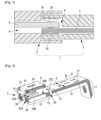
- the connector assembly 1 comprises a male connector 2 and a female connector 3.
- the male connector 2 has a housing made of dielectric material and which comprises a cavity 4 configured for accommodating at least one male power terminal 5.
- the female connector 3 has a housing made of dielectric material and which comprises a cavity 6 configured for accommodating at least one female power terminal 7.
- the female power terminal 7 comprises a terminal body 8 and a cage 9.
- the terminal body 8 comprises a contact portion 10, a connection portion 11 and an intermediate portion 12 between the two.
- the terminal body 8 has essentially a plate-like shape.
- the contact portion 10 and the intermediate portion 12 are aligned, whereas the connection portion 11 extends at right angle from the intermediate portion 12.
- the contact portion 10, the connection portion 11 and the intermediate portion 12 are formed as a multilayer structure.
- the contact portion 10 comprises eight conductive layers 13, whereas the connection portion 11 and the intermediate portion 12 comprise six conductive layers 13.
- each layer 13 is made of a copper alloy.
- Each layer 13 has a thickness of about 0.5 millimetre.
- Each layer 13 has a width W of about 35 millimetres.
- Each layer 13 has two main surfaces delimiting it a direction D corresponding to its thickness.
- the layers 13 are stacked in a direction D perpendicular to the main surfaces 14, 18 of the contact 10 and intermediate 12 portions.
- the contact portion 10 comprises a main top surface 14 and two contact areas 15 protruding from the main top surface 14. As shown in Figure 3 , each layer 13 of the contact portion 10 comprises two first embossed regions 16. The first embossed regions 16 of each layer 13 are registered with the first embossed regions 16 of an adjacent layer. The first embossed regions 16 of the top layer 13A respectively form a contact area 15. In the example illustrated in Figures 2 and 3 , the female power terminal 7 has two contact areas 15 (each corresponding respectively to a first embossed region 16). However, the contact portion 10 may comprise, in variations, only one contact area 15. Alternatively, as shown in Figure 4 , the contact portion 10 may comprise, in variations, more than two contact areas 15 (e.g. twelve contact areas 15 as shown in Figure 4 ).
- each layer 13 comprises at least one second embossed region 17.
- the female power terminal 7 has four second embossed regions 17.
- the intermediate region 12 may comprise, in variations, more or less than four second embossed regions 17 (e.g. eight second embossed regions 17 as shown in Figure 5 ).
- the second embossed regions 17 may result from embossing, from stamping or from another operation adapted for deforming the stacked layers 13. These operations (embossing, stamping or the like) mechanically couple the layers 13 together. They strengthen the multilayer structure and improve the electrical conductivity between adjacent layers 13.
- the second embossed regions 17 may be embossed or stamped from the main top surface 14 (see Figures 2 and 3 ) or from the main bottom surface 18.
- several second embossed regions 17 may be embossed or stamped from the main top surface 14 and others may be embossed or stamped from the main bottom surface 18 (in other words, each layer 13 of the plurality of conductive layers 13 comprises embossed or stamped regions 17 embossed or . stamped in opposite directions).
- the cage 9 is cut and shaped in a sheet metal (e.g. of stainless steel). As shown in Figures 2 and 3 , the cage 9 has a "U" shape, with a top wall 19 and a bottom wall 20, each respectively corresponding to a branch of the "U", and a lateral wall 21 joining the top 19 and bottom 20 walls.
- An elastic tongue 22 extends from the top wall 19 towards the bottom wall 20.
- the tongue 22 is configured so as to allow a male terminal 5 to be inserted between the top wall 19 and the main top surface 14 of the contact portion 10 of the female terminal 7. More particularly, the tongue 22 is configured for pressing a contact portion of the male terminal 5 against the contact areas 15.
- the cage 9 comprises hooks 23A, 23B, 23C configured for maintaining the cage 9 on the plurality of conductive layers 13 of the contact portion 10.
- the hooks 23A, 23B, 23C can also help to maintain the layers 13 assembled together.
- These front 23A and lateral 23B hooks do not cover the main top surface 14. Possibly, since the contact areas 15 protrude from the main top surface 14, the front hook 23A can stick-out further than the main top surface 14, while remaining below the top of the contact areas 15.
- the lateral hook 23B is advantageously flush with the main top surface 14.
- the cage 9 also comprise two rear hooks 23C which come back over the main top surface 14 and catch the layers 13 together.
- the rear hooks 23C may also serves for blocking a forward movement of the male terminal 5.
- Each rear hook 23C is inserted behind a shoulder 25 cut in the layers 13 and located behind the contact portion 10.
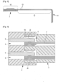
- Figures 6 to 8 show various versions of a set of female power terminals 7 (without cage).
- the three versions shown in Figures 6 to 8 differ from each other by the number of conductive layers 13 stacked in the intermediate portion 12 and the connection portion 11.
- Such a female power terminal 7 is adapted for conducting currents up to 450 Amps without exceeding 85°C.
- Such a female power terminal 7 is adapted for conducting currents up to 400 Amps without exceeding 85°C.
- the female power terminal 7 shown in Figure 8 comprises eight layers 13 in the contact portion 10, but only four layers in the intermediate portion 12 and in the connection portion 11.
- Such a female power terminal 7 is adapted for conducting currents up to 250 Amps without exceeding 85°C.
- the thickness of the contact portion 10 is greater than 3mm. It is advantageous to have a thicker portion where the contact between the male 5 and female 7 power terminals is. Indeed, the temperature may rise at the contact points (i.e. in the contact areas 15) more than elsewhere.
- the female power terminal 7 shown in Figure 6 has N conductive layers 13 stacked in the intermediate portion 12 and the connection portion 11.
- the number of conductive layers 13 stacked in the contact portion 10 is a positive integer N
- the number of conductive layers 13 stacked in the intermediate portion 12 and/or the connection portion 11 is N-n, where n is chosen as a positive integer lower a than N.
- the set of female power terminals 7 disclosed above has the advantage that it allows to adapt the number of conductive layers 13 (i.e. to adapt the cost) to the application, while keeping the same interface both for the male power terminal 5 and the male 2 and female 3 connectors.
- a connector for example a female connector 3, can accommodate one or several female power terminals 7 of this set of female terminals 7.
- this connector 3 accommodates several terminals 7, said several female power terminals 7 can be the same, said several female power terminals 7 can differ by the number of conductive layers 13 stacked in the intermediate portion 12 and the connection portion 11, whereas the number of conductive layers 13 stacked in the contact portion 10 are the same as shown in Figure 9 .
- the above disclosure relates to a female power terminal 7 but it can easily be transposed to male power terminals 5.
Landscapes
- Coupling Device And Connection With Printed Circuit (AREA)
Claims (10)
- Borne de puissance (5, 7) comprenant une partie de contact (10), une partie de connexion (11) et une partie intermédiaire (12) entre la partie de contact (10) et la partie de connexion (11), les parties de contact (10) et intermédiaire (12) comprenant une pluralité de couches conductrices (13) empilées le long d'une direction correspondant à leurs épaisseurs respectives, la partie de contact (10) comprenant une surface supérieure principale (14) et au moins une zone de contact (15) faisant saillie à partir de la surface supérieure principale (14),dans lequel chaque couche (13) de la pluralité de couches conductrices (13) dans la partie de contact (10) comprend au moins une première région embossée (16), ladite au moins une première région embossée (16) de chaque couche (13) étant alignée avec ladite au moins une première région embossée (16) d'une couche adjacente (13), et ladite au moins une première région embossée (16) d'une couche supérieure (13) formant ladite au moins une zone de contact (15),caractérisé par le fait que, dans la partie intermédiaire (12), chaque couche (13) de la pluralité de couches conductrices (13) comprend au moins une deuxième région embossée (17) qui couple mécaniquement les couches (13) entre elles .
- Borne de puissance (5, 7) selon la revendication 1, dans laquelle le nombre de couches conductrices (13) empilées dans la partie de contact (10) diffère du nombre de couches conductrices (13) empilées dans la partie intermédiaire (12) ou la partie de connexion (11).
- Borne de puissance (5, 7) selon l'une quelconque des revendications précédentes, dans laquelle chaque couche (13) de la pluralité de couches conductrices (13) comprend des régions embossées (16, 17) embossées dans des directions opposées.
- Borne de puissance (5, 7) selon l'une quelconque des revendications précédentes, dans laquelle l'épaisseur de la partie de contact (10) est supérieure à 3 mm.
- Borne de puissance (7) selon l'une quelconque des revendications précédentes, se présentant sous la forme d'une borne femelle (7) et comprenant une cage (9), la cage (9) présentant au moins une languette élastique (22) configurée pour presser une partie de contact d'une borne mâle (2) contre ladite au moins une zone de contact (15), et la cage (9) présentant au moins un crochet (23A, 23B, 23C) configuré pour maintenir la cage (9) sur la pluralité de couches conductrices (13) de la partie de contact (10) de la borne femelle (7).
- Ensemble de bornes de puissance (5, 7) comprenant au moins deux bornes (5, 7) selon l'une quelconque des revendications précédentes, dans lequel ces deux bornes (5, 7) diffèrent l'une de l'autre par le nombre de couches conductrices (13) empilées dans la partie intermédiaire (12) ou la partie de connexion (11), le nombre de couches conductrices (13) empilées dans la partie de contact (10) étant le même pour les deux bornes (5, 7).
- Ensemble de bornes de puissance (5, 7) selon la revendication 6, comprenant au moins trois bornes (5, 7), chacune ayant N couches conductrices (13) empilées dans la partie de contact (10), une ayant N couches conductrices (13) empilées dans la partie intermédiaire (12) ou la partie de connexion (11), une ayant N-2 couches conductrices (13) empilées dans la partie intermédiaire (12) ou la partie de connexion (11), et une ayant N-4 couches conductrices (13) empilées dans la partie intermédiaire (12) ou la partie de connexion (11).
- Ensemble de bornes d'alimentation (5, 7) selon la revendication 7, dans lequel les sections transversales des trois bornes (5, 7) sont respectivement d'environ 100 mm2, 75 mm2 et 50 mm2.
- Ensemble de bornes d'alimentation (5, 7) selon l'une des revendications 6 à 8, dans lequel la largeur de la partie de contact (10) de toutes les bornes (5, 7) est essentiellement la même.
- Connecteur comprenant au moins une borne de puissance (5, 7) logée dans une cavité (4, 6) formée dans un boîtier en matériau diélectrique, ladite au moins une borne de puissance (5, 7) étant choisie dans l'ensemble des bornes de puissance (5, 7) selon l'une quelconque des revendications 6 à 9.
Priority Applications (3)
| Application Number | Priority Date | Filing Date | Title |
|---|---|---|---|
| EP22315023.6A EP4220866B1 (fr) | 2022-01-26 | 2022-01-26 | Borne de puissance comportant une structure multicouche et ensemble de bornes de puissance ayant un nombre divers de couches |
| US18/081,101 US12424781B2 (en) | 2022-01-26 | 2022-12-14 | Power terminal with a multilayered structure and set of power terminals having various numbers of layers |
| CN202310000993.1A CN116505308A (zh) | 2022-01-26 | 2023-01-03 | 具有多层结构的电源端子和具有不同层数的电源端子集合 |
Applications Claiming Priority (1)
| Application Number | Priority Date | Filing Date | Title |
|---|---|---|---|
| EP22315023.6A EP4220866B1 (fr) | 2022-01-26 | 2022-01-26 | Borne de puissance comportant une structure multicouche et ensemble de bornes de puissance ayant un nombre divers de couches |
Publications (2)
| Publication Number | Publication Date |
|---|---|
| EP4220866A1 EP4220866A1 (fr) | 2023-08-02 |
| EP4220866B1 true EP4220866B1 (fr) | 2024-11-06 |
Family
ID=80775110
Family Applications (1)
| Application Number | Title | Priority Date | Filing Date |
|---|---|---|---|
| EP22315023.6A Active EP4220866B1 (fr) | 2022-01-26 | 2022-01-26 | Borne de puissance comportant une structure multicouche et ensemble de bornes de puissance ayant un nombre divers de couches |
Country Status (3)
| Country | Link |
|---|---|
| US (1) | US12424781B2 (fr) |
| EP (1) | EP4220866B1 (fr) |
| CN (1) | CN116505308A (fr) |
Families Citing this family (3)
| Publication number | Priority date | Publication date | Assignee | Title |
|---|---|---|---|---|
| EP4354663B1 (fr) * | 2022-10-13 | 2025-12-10 | AKNH Kontaktsysteme GmbH | Connecteur a sertir pour la connexion mecanique et electriquement conductrice d'un contact de connexion electrique a un conducteur electrique et connexion a sertir d'un contact de connexion electrique a un conducteur electrique |
| DE102024123576A1 (de) * | 2024-08-19 | 2026-02-19 | Schaeffler Technologies AG & Co. KG | Multilayerkontakt für eine Hochvoltkomponente |
| DE102024123577A1 (de) * | 2024-08-19 | 2026-02-19 | Schaeffler Technologies AG & Co. KG | Multilayerkontakt für eine Hochvoltkomponente eines Kraftfahrzeugs |
Family Cites Families (16)
| Publication number | Priority date | Publication date | Assignee | Title |
|---|---|---|---|---|
| DE472550C (de) * | 1929-03-04 | Voigt & Haeffner Akt Ges | Sammelschiene fuer zu vergiessende Schaltanlagen | |
| US4685019A (en) * | 1985-04-29 | 1987-08-04 | Engelhard Corporation | Controlled electrical contacts for electrical switchgear |
| US4891618A (en) * | 1988-08-01 | 1990-01-02 | Westinghouse Electric Corp. | Laminated copper assembly |
| US7104812B1 (en) * | 2005-02-24 | 2006-09-12 | Molex Incorporated | Laminated electrical terminal |
| WO2010037410A1 (fr) * | 2008-10-03 | 2010-04-08 | Abb Technology Ag | Connecteur stratifié |
| US8721368B2 (en) | 2011-10-06 | 2014-05-13 | Tyco Electronics Corporation | Power terminal connector and system |
| WO2015048085A1 (fr) | 2013-09-25 | 2015-04-02 | Tyco Electronics Corporation | Connecteur de borne électrique |
| US10389055B1 (en) * | 2018-06-20 | 2019-08-20 | Delphia Technologies, Llc | Electrical connector assembly |
| US11355902B2 (en) | 2019-01-28 | 2022-06-07 | TE Connectivity Services Gmbh | Power connector for a bus bar |
| FR3094578B1 (fr) * | 2019-04-01 | 2021-12-10 | Aptiv Tech Ltd | Dispositif de connexion de puissance pour batterie électrique et ensemble de connexion comprenant ce dispositif. |
| KR20210045320A (ko) | 2019-10-16 | 2021-04-26 | 타이코에이엠피 주식회사 | 플렉서블 케이블용 터미널 어셈블리 |
| US11264752B1 (en) | 2020-11-09 | 2022-03-01 | Aptiv Technologies Limited | Planar terminal connector having an additional contact spring |
| US11387586B2 (en) | 2020-11-09 | 2022-07-12 | Aptiv Technologies Limited | High voltage (HV) terminal frame and method of manufacturing the same |
| CN117913571A (zh) | 2020-12-30 | 2024-04-19 | 泰科电子(上海)有限公司 | 端子组件和连接器 |
| US12003052B2 (en) | 2021-03-02 | 2024-06-04 | Aptiv Technologies AG | Female electrical bus bar connector and method of forming same |
| US20220368052A1 (en) | 2021-05-12 | 2022-11-17 | Aptiv Technologies Limited | High voltage (hv) terminal frame |
-
2022
- 2022-01-26 EP EP22315023.6A patent/EP4220866B1/fr active Active
- 2022-12-14 US US18/081,101 patent/US12424781B2/en active Active
-
2023
- 2023-01-03 CN CN202310000993.1A patent/CN116505308A/zh active Pending
Also Published As
| Publication number | Publication date |
|---|---|
| US12424781B2 (en) | 2025-09-23 |
| CN116505308A (zh) | 2023-07-28 |
| US20230246371A1 (en) | 2023-08-03 |
| EP4220866A1 (fr) | 2023-08-02 |
Similar Documents
| Publication | Publication Date | Title |
|---|---|---|
| EP4220866B1 (fr) | Borne de puissance comportant une structure multicouche et ensemble de bornes de puissance ayant un nombre divers de couches | |
| EP2929596B1 (fr) | Connecteur de borne de puissance | |
| US6077131A (en) | Male terminal | |
| EP4125158B1 (fr) | Structure pour connexion électrique | |
| JP6449255B2 (ja) | 電力端子コネクタ | |
| WO2012043486A1 (fr) | Connecteur de détection de tension de cellule | |
| CN103515892A (zh) | 电气连接箱 | |
| US20200006885A1 (en) | Stacked connector and wire harness | |
| JP2006310007A (ja) | ワイヤハーネスの組立方法、ワイヤハーネス及びコネクタ | |
| CN113875095B (zh) | 连接端子及连接器 | |
| JP2013171617A (ja) | 電池用配線モジュール | |
| JP7753286B2 (ja) | コネクタ製造装置 | |
| US6626693B2 (en) | Metal terminal and method of forming metal terminal | |
| JP4014881B2 (ja) | 電気接続装置 | |
| EP3916918A1 (fr) | Procédé de formation d'une connexion entre une barre omnibus et une section de contact, barre omnibus ayant une section de contact et système de distribution de puissance ayant une telle barre omnibus | |
| CN102763242A (zh) | 电池组件用电极结构体 | |
| JP4805729B2 (ja) | 端子金具同士の固定方法及び端子金具 | |
| EP1006614A2 (fr) | Organe de contact à pression et son boítier | |
| EP4343972A1 (fr) | Système d'interconnexion de puissance | |
| EP4002591B1 (fr) | Borne de puissance avec une partie de sertissage améliorée et méthode de sertissage associée | |
| JP7769883B2 (ja) | 配線モジュール | |
| JP2026026637A (ja) | 導通部材 | |
| JP2005129390A (ja) | 中継端子 | |
| JP3746951B2 (ja) | プレート状絶縁体 | |
| JP2025020733A (ja) | バスバー及び配線モジュール |
Legal Events
| Date | Code | Title | Description |
|---|---|---|---|
| PUAI | Public reference made under article 153(3) epc to a published international application that has entered the european phase |
Free format text: ORIGINAL CODE: 0009012 |
|
| STAA | Information on the status of an ep patent application or granted ep patent |
Free format text: STATUS: REQUEST FOR EXAMINATION WAS MADE |
|
| 17P | Request for examination filed |
Effective date: 20230224 |
|
| AK | Designated contracting states |
Kind code of ref document: A1 Designated state(s): AL AT BE BG CH CY CZ DE DK EE ES FI FR GB GR HR HU IE IS IT LI LT LU LV MC MK MT NL NO PL PT RO RS SE SI SK SM TR |
|
| GRAP | Despatch of communication of intention to grant a patent |
Free format text: ORIGINAL CODE: EPIDOSNIGR1 |
|
| STAA | Information on the status of an ep patent application or granted ep patent |
Free format text: STATUS: GRANT OF PATENT IS INTENDED |
|
| RIC1 | Information provided on ipc code assigned before grant |
Ipc: H01R 11/01 20060101ALN20240508BHEP Ipc: H01R 13/18 20060101ALN20240508BHEP Ipc: H01R 13/11 20060101AFI20240508BHEP |
|
| INTG | Intention to grant announced |
Effective date: 20240527 |
|
| GRAS | Grant fee paid |
Free format text: ORIGINAL CODE: EPIDOSNIGR3 |
|
| GRAA | (expected) grant |
Free format text: ORIGINAL CODE: 0009210 |
|
| STAA | Information on the status of an ep patent application or granted ep patent |
Free format text: STATUS: THE PATENT HAS BEEN GRANTED |
|
| RAP1 | Party data changed (applicant data changed or rights of an application transferred) |
Owner name: APTIV TECHNOLOGIES AG |
|
| RAP3 | Party data changed (applicant data changed or rights of an application transferred) |
Owner name: APTIV TECHNOLOGIES AG |
|
| AK | Designated contracting states |
Kind code of ref document: B1 Designated state(s): AL AT BE BG CH CY CZ DE DK EE ES FI FR GB GR HR HU IE IS IT LI LT LU LV MC MK MT NL NO PL PT RO RS SE SI SK SM TR |
|
| REG | Reference to a national code |
Ref country code: GB Ref legal event code: FG4D |
|
| P01 | Opt-out of the competence of the unified patent court (upc) registered |
Free format text: CASE NUMBER: APP_55354/2024 Effective date: 20241009 |
|
| REG | Reference to a national code |
Ref country code: CH Ref legal event code: EP |
|
| REG | Reference to a national code |
Ref country code: DE Ref legal event code: R096 Ref document number: 602022007497 Country of ref document: DE |
|
| REG | Reference to a national code |
Ref country code: IE Ref legal event code: FG4D |
|
| REG | Reference to a national code |
Ref country code: LT Ref legal event code: MG9D |
|
| REG | Reference to a national code |
Ref country code: NL Ref legal event code: MP Effective date: 20241106 |
|
| PG25 | Lapsed in a contracting state [announced via postgrant information from national office to epo] |
Ref country code: IS Free format text: LAPSE BECAUSE OF FAILURE TO SUBMIT A TRANSLATION OF THE DESCRIPTION OR TO PAY THE FEE WITHIN THE PRESCRIBED TIME-LIMIT Effective date: 20250306 Ref country code: PT Free format text: LAPSE BECAUSE OF FAILURE TO SUBMIT A TRANSLATION OF THE DESCRIPTION OR TO PAY THE FEE WITHIN THE PRESCRIBED TIME-LIMIT Effective date: 20250306 Ref country code: HR Free format text: LAPSE BECAUSE OF FAILURE TO SUBMIT A TRANSLATION OF THE DESCRIPTION OR TO PAY THE FEE WITHIN THE PRESCRIBED TIME-LIMIT Effective date: 20241106 |
|
| PG25 | Lapsed in a contracting state [announced via postgrant information from national office to epo] |
Ref country code: FI Free format text: LAPSE BECAUSE OF FAILURE TO SUBMIT A TRANSLATION OF THE DESCRIPTION OR TO PAY THE FEE WITHIN THE PRESCRIBED TIME-LIMIT Effective date: 20241106 Ref country code: NL Free format text: LAPSE BECAUSE OF FAILURE TO SUBMIT A TRANSLATION OF THE DESCRIPTION OR TO PAY THE FEE WITHIN THE PRESCRIBED TIME-LIMIT Effective date: 20241106 |
|
| REG | Reference to a national code |
Ref country code: AT Ref legal event code: MK05 Ref document number: 1740437 Country of ref document: AT Kind code of ref document: T Effective date: 20241106 |
|
| PG25 | Lapsed in a contracting state [announced via postgrant information from national office to epo] |
Ref country code: BG Free format text: LAPSE BECAUSE OF FAILURE TO SUBMIT A TRANSLATION OF THE DESCRIPTION OR TO PAY THE FEE WITHIN THE PRESCRIBED TIME-LIMIT Effective date: 20241106 |
|
| PG25 | Lapsed in a contracting state [announced via postgrant information from national office to epo] |
Ref country code: ES Free format text: LAPSE BECAUSE OF FAILURE TO SUBMIT A TRANSLATION OF THE DESCRIPTION OR TO PAY THE FEE WITHIN THE PRESCRIBED TIME-LIMIT Effective date: 20241106 |
|
| PG25 | Lapsed in a contracting state [announced via postgrant information from national office to epo] |
Ref country code: NO Free format text: LAPSE BECAUSE OF FAILURE TO SUBMIT A TRANSLATION OF THE DESCRIPTION OR TO PAY THE FEE WITHIN THE PRESCRIBED TIME-LIMIT Effective date: 20250206 |
|
| PG25 | Lapsed in a contracting state [announced via postgrant information from national office to epo] |
Ref country code: AT Free format text: LAPSE BECAUSE OF FAILURE TO SUBMIT A TRANSLATION OF THE DESCRIPTION OR TO PAY THE FEE WITHIN THE PRESCRIBED TIME-LIMIT Effective date: 20241106 Ref country code: LV Free format text: LAPSE BECAUSE OF FAILURE TO SUBMIT A TRANSLATION OF THE DESCRIPTION OR TO PAY THE FEE WITHIN THE PRESCRIBED TIME-LIMIT Effective date: 20241106 Ref country code: GR Free format text: LAPSE BECAUSE OF FAILURE TO SUBMIT A TRANSLATION OF THE DESCRIPTION OR TO PAY THE FEE WITHIN THE PRESCRIBED TIME-LIMIT Effective date: 20250207 |
|
| PG25 | Lapsed in a contracting state [announced via postgrant information from national office to epo] |
Ref country code: PL Free format text: LAPSE BECAUSE OF FAILURE TO SUBMIT A TRANSLATION OF THE DESCRIPTION OR TO PAY THE FEE WITHIN THE PRESCRIBED TIME-LIMIT Effective date: 20241106 |
|
| PG25 | Lapsed in a contracting state [announced via postgrant information from national office to epo] |
Ref country code: RS Free format text: LAPSE BECAUSE OF FAILURE TO SUBMIT A TRANSLATION OF THE DESCRIPTION OR TO PAY THE FEE WITHIN THE PRESCRIBED TIME-LIMIT Effective date: 20250206 |
|
| PG25 | Lapsed in a contracting state [announced via postgrant information from national office to epo] |
Ref country code: SM Free format text: LAPSE BECAUSE OF FAILURE TO SUBMIT A TRANSLATION OF THE DESCRIPTION OR TO PAY THE FEE WITHIN THE PRESCRIBED TIME-LIMIT Effective date: 20241106 |
|
| PG25 | Lapsed in a contracting state [announced via postgrant information from national office to epo] |
Ref country code: DK Free format text: LAPSE BECAUSE OF FAILURE TO SUBMIT A TRANSLATION OF THE DESCRIPTION OR TO PAY THE FEE WITHIN THE PRESCRIBED TIME-LIMIT Effective date: 20241106 |
|
| PG25 | Lapsed in a contracting state [announced via postgrant information from national office to epo] |
Ref country code: EE Free format text: LAPSE BECAUSE OF FAILURE TO SUBMIT A TRANSLATION OF THE DESCRIPTION OR TO PAY THE FEE WITHIN THE PRESCRIBED TIME-LIMIT Effective date: 20241106 |
|
| PG25 | Lapsed in a contracting state [announced via postgrant information from national office to epo] |
Ref country code: RO Free format text: LAPSE BECAUSE OF FAILURE TO SUBMIT A TRANSLATION OF THE DESCRIPTION OR TO PAY THE FEE WITHIN THE PRESCRIBED TIME-LIMIT Effective date: 20241106 |
|
| PG25 | Lapsed in a contracting state [announced via postgrant information from national office to epo] |
Ref country code: SK Free format text: LAPSE BECAUSE OF FAILURE TO SUBMIT A TRANSLATION OF THE DESCRIPTION OR TO PAY THE FEE WITHIN THE PRESCRIBED TIME-LIMIT Effective date: 20241106 |
|
| PG25 | Lapsed in a contracting state [announced via postgrant information from national office to epo] |
Ref country code: CZ Free format text: LAPSE BECAUSE OF FAILURE TO SUBMIT A TRANSLATION OF THE DESCRIPTION OR TO PAY THE FEE WITHIN THE PRESCRIBED TIME-LIMIT Effective date: 20241106 |
|
| PG25 | Lapsed in a contracting state [announced via postgrant information from national office to epo] |
Ref country code: IT Free format text: LAPSE BECAUSE OF FAILURE TO SUBMIT A TRANSLATION OF THE DESCRIPTION OR TO PAY THE FEE WITHIN THE PRESCRIBED TIME-LIMIT Effective date: 20241106 |
|
| REG | Reference to a national code |
Ref country code: DE Ref legal event code: R097 Ref document number: 602022007497 Country of ref document: DE |
|
| REG | Reference to a national code |
Ref country code: CH Ref legal event code: PL |
|
| PG25 | Lapsed in a contracting state [announced via postgrant information from national office to epo] |
Ref country code: SE Free format text: LAPSE BECAUSE OF FAILURE TO SUBMIT A TRANSLATION OF THE DESCRIPTION OR TO PAY THE FEE WITHIN THE PRESCRIBED TIME-LIMIT Effective date: 20241106 |
|
| PLBE | No opposition filed within time limit |
Free format text: ORIGINAL CODE: 0009261 |
|
| STAA | Information on the status of an ep patent application or granted ep patent |
Free format text: STATUS: NO OPPOSITION FILED WITHIN TIME LIMIT |
|
| PG25 | Lapsed in a contracting state [announced via postgrant information from national office to epo] |
Ref country code: LU Free format text: LAPSE BECAUSE OF NON-PAYMENT OF DUE FEES Effective date: 20250126 Ref country code: MC Free format text: LAPSE BECAUSE OF FAILURE TO SUBMIT A TRANSLATION OF THE DESCRIPTION OR TO PAY THE FEE WITHIN THE PRESCRIBED TIME-LIMIT Effective date: 20241106 |
|
| 26N | No opposition filed |
Effective date: 20250807 |
|
| PG25 | Lapsed in a contracting state [announced via postgrant information from national office to epo] |
Ref country code: BE Free format text: LAPSE BECAUSE OF NON-PAYMENT OF DUE FEES Effective date: 20250131 |
|
| PG25 | Lapsed in a contracting state [announced via postgrant information from national office to epo] |
Ref country code: CH Free format text: LAPSE BECAUSE OF NON-PAYMENT OF DUE FEES Effective date: 20250131 |
|
| REG | Reference to a national code |
Ref country code: BE Ref legal event code: MM Effective date: 20250131 |
|
| PG25 | Lapsed in a contracting state [announced via postgrant information from national office to epo] |
Ref country code: IE Free format text: LAPSE BECAUSE OF NON-PAYMENT OF DUE FEES Effective date: 20250126 |
|
| PGFP | Annual fee paid to national office [announced via postgrant information from national office to epo] |
Ref country code: GB Payment date: 20260112 Year of fee payment: 5 |
|
| PGFP | Annual fee paid to national office [announced via postgrant information from national office to epo] |
Ref country code: DE Payment date: 20251217 Year of fee payment: 5 |
|
| PGFP | Annual fee paid to national office [announced via postgrant information from national office to epo] |
Ref country code: FR Payment date: 20260107 Year of fee payment: 5 |