EP4220944B1 - Elektronische schaltung zur hüllkurvendetektion und demodulator dafür - Google Patents
Elektronische schaltung zur hüllkurvendetektion und demodulator dafür Download PDFInfo
- Publication number
- EP4220944B1 EP4220944B1 EP23163078.1A EP23163078A EP4220944B1 EP 4220944 B1 EP4220944 B1 EP 4220944B1 EP 23163078 A EP23163078 A EP 23163078A EP 4220944 B1 EP4220944 B1 EP 4220944B1
- Authority
- EP
- European Patent Office
- Prior art keywords
- signal
- ser
- input signal
- coupled
- transistor
- Prior art date
- Legal status (The legal status is an assumption and is not a legal conclusion. Google has not performed a legal analysis and makes no representation as to the accuracy of the status listed.)
- Active
Links
Images


Classifications
-
- G—PHYSICS
- G01—MEASURING; TESTING
- G01R—MEASURING ELECTRIC VARIABLES; MEASURING MAGNETIC VARIABLES
- G01R19/00—Arrangements for measuring currents or voltages or for indicating presence or sign thereof
- G01R19/04—Measuring peak values or amplitude or envelope of AC or of pulses
-
- H—ELECTRICITY
- H03—ELECTRONIC CIRCUITRY
- H03D—DEMODULATION OR TRANSFERENCE OF MODULATION FROM ONE CARRIER TO ANOTHER
- H03D1/00—Demodulation of amplitude-modulated oscillations
- H03D1/02—Details
- H03D1/06—Modifications of demodulators to reduce distortion, e.g. by negative feedback
-
- H—ELECTRICITY
- H03—ELECTRONIC CIRCUITRY
- H03D—DEMODULATION OR TRANSFERENCE OF MODULATION FROM ONE CARRIER TO ANOTHER
- H03D1/00—Demodulation of amplitude-modulated oscillations
- H03D1/14—Demodulation of amplitude-modulated oscillations by means of non-linear elements having more than two poles
- H03D1/18—Demodulation of amplitude-modulated oscillations by means of non-linear elements having more than two poles of semiconductor devices
-
- H—ELECTRICITY
- H03—ELECTRONIC CIRCUITRY
- H03D—DEMODULATION OR TRANSFERENCE OF MODULATION FROM ONE CARRIER TO ANOTHER
- H03D1/00—Demodulation of amplitude-modulated oscillations
- H03D1/22—Homodyne or synchrodyne circuits
- H03D1/2245—Homodyne or synchrodyne circuits using two quadrature channels
-
- H—ELECTRICITY
- H03—ELECTRONIC CIRCUITRY
- H03D—DEMODULATION OR TRANSFERENCE OF MODULATION FROM ONE CARRIER TO ANOTHER
- H03D3/00—Demodulation of angle-, frequency- or phase- modulated oscillations
-
- H—ELECTRICITY
- H04—ELECTRIC COMMUNICATION TECHNIQUE
- H04L—TRANSMISSION OF DIGITAL INFORMATION, e.g. TELEGRAPHIC COMMUNICATION
- H04L27/00—Modulated-carrier systems
- H04L27/02—Amplitude-modulated carrier systems, e.g. using on-off keying; Single sideband or vestigial sideband modulation
- H04L27/06—Demodulator circuits; Receiver circuits
-
- H—ELECTRICITY
- H04—ELECTRIC COMMUNICATION TECHNIQUE
- H04L—TRANSMISSION OF DIGITAL INFORMATION, e.g. TELEGRAPHIC COMMUNICATION
- H04L27/00—Modulated-carrier systems
- H04L27/18—Phase-modulated carrier systems, i.e. using phase-shift keying
- H04L27/22—Demodulator circuits; Receiver circuits
- H04L27/233—Demodulator circuits; Receiver circuits using non-coherent demodulation
- H04L27/2332—Demodulator circuits; Receiver circuits using non-coherent demodulation using a non-coherent carrier
-
- H—ELECTRICITY
- H03—ELECTRONIC CIRCUITRY
- H03F—AMPLIFIERS
- H03F3/00—Amplifiers with only discharge tubes or only semiconductor devices as amplifying elements
- H03F3/20—Power amplifiers, e.g. Class B amplifiers, Class C amplifiers
Definitions
- Embodiments of the invention relate to electronic circuits, more particularly to electronic envelope detection circuits capable of being incorporated into radio frequency demodulators for wireless communication applications.
- an electronic envelope detection circuit aims to extract a low frequency signal from a carrier signal, for example a radio frequency carrier signal, modulated in amplitude.
- Envelope detectors are generally used in amplitude-shift keying demodulators, commonly known to those skilled in the art by the English acronym: ASK (“Amplitude-Shift Keying” in English).
- This type of demodulator is capable of processing a high data rate, for example of the order of several gigabits per second, and of performing non-coherent demodulations while allowing low consumption.
- These technical characteristics are particularly advantageous for wireless communication applications, for example short-range millimeter-wave wireless connections ("Short-Range millimeter-wave wireless link" in English).
- Patent documents US 2017/343589 A1 , US 2008/084956 A1 , CN 106 712 729 A , JP S57 79715 A , EP 2 713 171 A2 disclose examples of conventional envelope detectors.
- a classical envelope detector may for example be based on the nonlinearity of an electronic device and may include an amplifier in a common source configuration.
- the amplifier of such an envelope detector requires a precise biasing point in order to maximize the conversion gain and has a fairly limited dynamic range.
- This bias point is important so that the average power of a radio frequency input signal of the envelope detector does not exceed the dynamic range of the envelope detector in order to extract a low frequency signal with sufficient amplitude but without clipping.
- the conversion gain i.e. the sensitivity
- the dynamic range of the envelope detector cannot be maximized.
- the average power of the radio frequency input signal varies, this often results in distortion of the envelope detector output signal.
- an electronic envelope detection circuit according to claim 1.
- Such a detection stage allows the input signal to be received through a single input (“single ended mode” in English).
- control signal advantageously corresponds to the average of the gate bias voltage of said at least one transistor.
- the input signal advantageously controls the instantaneous value of this grid bias voltage.
- such a circuit advantageously makes it possible to adapt the polarization of the detection stage to the average power of the received signal, i.e. the input signal, and thus increase the reception dynamics.
- such a circuit advantageously allows, as a function of the variation of the average power of the input signal, a dynamic adjustment of the polarization point of said at least one transistor of the detection stage so as to adapt the polarization point of said at least one transistor to the average power of the radiofrequency input signal.
- the conversion gain of said electronic envelope detection circuit is dynamically adapted to the variation of the average power of the input signal.
- said bias point is more or less adapted and little influenced by said variation.
- the envelope detection electronic circuit can dynamically adapt to the variation of the average power of the input signal and the dynamic range of the envelope detection electronic circuit is extended.
- the processing stage may for example include a transimpedance amplifier intended to receive the internal signal.
- the frequency of the radio frequency input signal can for example be of the order of 60 GHz.
- a demodulator incorporating an electronic envelope detection circuit as defined above.
- the demodulator may for example be an amplitude shift keying type demodulator.
- a wireless radio frequency receiver comprising a demodulator as defined above.
- a wireless communication apparatus comprising a radio frequency receiver as defined above.
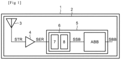
- FIG. 1 illustrates a wireless communication device 1, here for example based on short-range millimeter-wave wireless link technology.
- This device 1 is configured to perform high-speed wireless communications, for example several gigabits per second over a short range, for example of the order of 10 centimeters, so as to replace data communications via cables, for example of the universal serial bus type, commonly known to those skilled in the art by the English acronym USB (“Universal Serial Bus” in English).
- high-speed wireless communications for example several gigabits per second over a short range, for example of the order of 10 centimeters
- USB Universal Serial Bus
- the device 1 can advantageously be used for small footprint and/or sealed industrial or consumer devices.
- the demodulator 5 comprises an electronic envelope detection circuit 6 and a baseband amplifier ABB (“Baseband Amplifier” in English).
- ABB Baseband Amplifier
- the electronic envelope detection circuit 6 is intended to receive the input signal SER and configured to deliver to the baseband amplifier ABB, a low frequency output signal SSB.
- the baseband amplifier is configured to then amplify the low frequency SSB output signal to generate the SBB output signal.
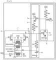
- FIG 2 We refer to the figure 2 to illustrate in more detail a preferred embodiment of the electronic envelope detection circuit 6 comprising a detection stage 7 and a processing stage 8.
- the SER radio frequency input signal can also be applied differentially across the winding terminals.
- the first output winding ES1 comprises a first middle node NM1 located in the middle of the first output winding ES1 and coupled to the processing stage 8.
- the first middle node NM1 is intended to receive a control signal SC delivered by the processing stage 8.
- the first output winding ES1 is configured to deliver to the gates G1, G2 of the first and second transistors T1, T2 a differential gate voltage from the input signal SER and the control signal SC.
- the bias point of the first and second transistors T1, T2 is controlled by the input signal SER and the control signal SC.
- control signal SC is a voltage signal intended to adjust the average power, in common mode, of the radiofrequency input signal SER.
- the second output winding ES2 has a second middle node NM2 located in the middle of the two output windings ES2 and coupled to ground GND.
- the second output winding ES2 is configured to supply to the sources S1, S2 of the first and second transistors T1, T2 a differential source voltage from the input signal SER.
- turns directions of the input winding EE1 and the first output winding ES1 are identical while the turns direction of the second winding is opposite to that of the input winding EE1 and the first output winding ES1.
- the number of turns NSS1 of the first output winding ES1 is greater than the number of turns NSE of the input winding EE and than the number of turns NSS of the second output winding ES2 so as to increase the sensitivity of the detection stage 7.
- the detection stage 7 further comprises an intermediate node NI coupled to the drains D1, D2 of the first and second transistors T1, T2 and the detection stage 7 is configured to deliver to the intermediate node NI an internal current signal SI which is the combination of the drain currents of the first and second transistors T1, T2.
- the processing stage 8 comprises an output module 9 and a feedback module 10.
- the output module 9 comprises a transimpedance amplifier AT commonly known to those skilled in the art.
- the transimpedance amplifier AT here comprises, for example, a third N-type MOS transistor T3 whose gate G3 is coupled to the intermediate node NI, whose source S3 is coupled to ground GND, and whose drain D3 is coupled to an output terminal BS, and an output resistor RS coupled between a supply voltage VCC and the output terminal BS.
- the size of the third transistor T3 is suitably chosen to match those of the first and second transistors T1 and T2 so as to ensure that the gate voltage VG3 of the third transistor T3 is suitable for operating the first and second transistors T1 and T2.
- the drain current of the third transistor T3 is approximately proportional to the internal signal SI.
- the output module 9 is configured to convert the drain current into the low-frequency output signal SSB into a voltage on the output terminal BS via the output resistor RS.
- the transimpedance amplifier AT is configured to deliver to the output terminal BS the low-frequency output signal SSB in voltage from the internal signal SI in current.
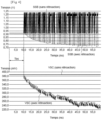
- the carrier frequency of the SER input signal is here for example 60 GHz and the SER input signal is modulated by a 5Gb/s bit stream in amplitude-shift keying (ASK).
- ASK amplitude-shift keying
- the source voltages VS1, VS2 of the first and second transistors T1, T2 are shown below the input signal SER.
- the amplitude of the source voltage VS2 of the second transistor T2 is substantially identical to that of the input signal SER while the amplitude of the source voltage VS1 of the first transistor T1 is substantially opposite to that of the input signal SER.
- the amplitude of the gate voltage VG1 of the first transistor T1 is greater than that of the input signal SER while the amplitude of the gate voltage VG2 of the second transistor T2 is substantially opposite to that of the first transistor T1.
- VSC value of the control signal SC corresponds to the average of the gate voltages VG1, VG2 of the first and second transistors T1, T2.
- the value of the internal signal SI and the value of the low-frequency output signal SSB will also decrease while the VSC value of the control signal SC will increase so as to compensate for the variation in the average power of the input signal SER.
- the value of the SSB output signal is constant (DC value) because that of the SER input signal is zero.
- the average power of the input signal SER is then increased so as to increase the values of the drain currents of the first and second transistors T1, T2.
- the value of the internal signal SI is consequently increased.
- Output module 9 is configured to generate the voltage output signal SSB from the internal signal SI.
- the value of the SSB output signal is therefore also increased so as to increase the value of the source current of the fourth transistor T4.
- the value of the SSB output signal is saturated here because the amplitude of the SER input signal is already too large.
- the gain of the transimpedance amplifier is limited, here for example by the values of the feedback resistor RR and the dimensions of the MOS transistor T4 as well as by the open loop gain given by the third transistor T3 and the output resistor RS, the average gate voltage VG3 of the third transistor T3 and the value VSC of the control signal SC will consequently decrease, and this all the more so as the output BS of the output module 9 approaches saturation, which has the effect of reducing the open loop gain formed by the third transistor T3 and the output resistor RS.
- the value VSC of the control signal SC corresponds to the average of the gate voltages VG1, VG2 of the first and second transistors T1, T2.
- the decrease in said value VSC of the control signal SC leads to the decrease in the average of the gate voltages VG1, VG2 of the first and second transistors T1, T2.
- the bias point of the detection stage is decreased by following the variation of the VSC value of the SC control signal.
- the variation range of the SSB output signal is extended and the value of the SSB output signal oscillates around its continuous value (DC), which advantageously allows better demodulation quality, in particular for restoring a binary signal by comparing the SSB output signal to a threshold close to its continuous value (DC), and reduced distortion at the level of the low-frequency SSB output signal.
- DC continuous value
- Such distortion can degrade the jitter of the demodulated binary signal.
- this electronic envelope detection circuit 6 can for example have the same processing stage 8 illustrated in the figure 2 .
- the detection stage 7 of this electronic envelope detection circuit 6 comprises a fifth N-type MOS transistor T5 whose drain D5 is coupled to the intermediate node NI connected to the gate G3 of the third transistor T3, whose source S5 is coupled to ground via an input winding EE of a dual-channel transformer T2V, and whose gate G5 is coupled to the feedback module 10 via an output winding ES of the transformer T2V.
- the detection stage 7 receives the radio frequency input signal SER at the source S5 of the fifth transistor T5.
- the direction of turns of the input winding EE is opposite to that of turns of the output winding ES.
- the number of turns of the input winding EE is for example less than that of the turns of the output winding ES so as to improve the sensitivity of the detection stage 7.
- the gate voltage VG5 of the fifth transistor T5 is controlled by the input signal SER.
- the output winding ES is also intended to receive the control signal SC delivered by the processing stage 8.
- the gate voltage VG5 of the fifth transistor T5 is also controlled by the control signal SC.
- the bias point of the fifth transistor T5 is therefore controlled by the input signal SER and by the control signal SC.
- the drain current of the fifth transistor T5 i.e. the internal signal SI, also increases.
- the processing stage 8 is configured to increase the value of the output signal SSB and decrease the value of the control signal SC so as to decrease the average of the gate voltage VG5 of the fifth transistor T5.
- the electronic envelope detection circuit 6 is capable of adapting to the variation of the average power of the signal SER input so as to dynamically modify the bias point and the conversion gain of the detection stage 7.
- the dynamic range of said circuit 6 is therefore also extended.
- Processing stage 8 is similar to that shown in the figures 2 And 5 and the detection stage 7 comprises a sixth N-type MOS transistor T6 and a seventh N-type MOS transistor T7.
- the drains of the sixth and seventh transistors T6, T7 are jointly coupled to the intermediate node NI so as to deliver to said intermediate node NI the internal signal SI.
- the sources of the sixth and seventh transistors T6, T7 are coupled to ground GND.
- the gate G6 of the sixth transistor T6 is coupled to the intermediate node NI via a first control resistor RC1 and the gate G6 of the sixth transistor T6 is further coupled to a first input terminal BE1 via a first capacitor C1.
- the gate G7 of the seventh transistor T7 is coupled to the intermediate node NI via a second control resistor RC2.
- the gate G7 of the seventh transistor T7 is further coupled to a second input terminal BE2 via a second capacitor C2.
- the first and second control resistors RC1, RC2 are identical and the gates G6, G7 of the sixth and seventh transistors T6, T7 are intended to receive the same control signal SC.
- the detection stage 7 is configured to receive the radio frequency input signal SER in differential via the first and second capacitors C1, C2.
- the output module 9 is configured to convert the internal signal SI into the output signal SSB and the value of the output signal SSB also decreases, which leads to an increase in the gate voltage VG3 of the third transistor T3.
- control signal SC is therefore increased so as to modify the bias point of the detection stage 6.
- an electronic envelope detection circuit capable of dynamically adapting the bias point and the conversion gain of said circuit to the variation of the average power of the input signal of said electronic envelope detection circuit so as to extend its dynamic range.
Landscapes
- Engineering & Computer Science (AREA)
- Power Engineering (AREA)
- Physics & Mathematics (AREA)
- Computer Networks & Wireless Communication (AREA)
- Signal Processing (AREA)
- Nonlinear Science (AREA)
- General Physics & Mathematics (AREA)
- Amplifiers (AREA)
- Digital Transmission Methods That Use Modulated Carrier Waves (AREA)
Claims (7)
- Elektronische Hüllkurven-Detektionsschaltung, umfassend eine Detektionsstufe (7), die mindestens einen MOS-Transistor (T1, T2, T5, T6, T7) umfasst, der so konfiguriert ist, dass er ein Funkfrequenz-Eingangssignal (SER) empfängt und ein internes Signal (SI) auf Grundlage des Eingangssignals (SER) bereitstellt, wobei die mittlere Gate-Vorspannung des mindestens einen Transistors (T1, T2, T5, T6, T7) durch ein Ansteuersignal (SC) gesteuert wird, undeine Verarbeitungsstufe (8), die mit der Detektionsstufe (7) gekoppelt und so konfiguriert ist, dass sie ein Niederfrequenz-Ausgangssignal (SSB) auf Grundlage des internen Signals (SI) bereitstellt und das Ansteuersignal (SC) auf Grundlage des internen Signals (SI) so bereitstellt, dass der Wert des Ansteuersignals (SC) abnimmt, wenn die mittlere Leistung des Eingangssignals (SER) zunimmt, und umgekehrt,dadurch gekennzeichnet, dassdie Detektionsstufe (7) umfasst:einen MOS-Transistor (T5) vom N-Typ, dessen Drain (D5) mit der Verarbeitungsstufe (8) gekoppelt ist, undeinen Transformator (T2V), der eine Eingangswicklung (EE), die dazu bestimmt ist, das Eingangssignal (SER) zu empfangen, und zwischen die Source (S5) des MOS-Transistors (T5) vom N-Typ und die Masse (GND) gekoppelt ist, und eine Ausgangswicklung (ES) umfasst, die zwischen das Gate (G5) des MOS-Transistors (T5) vom N-Typ und die Verarbeitungsstufe (8) gekoppelt und dazu bestimmt ist, das Ansteuersignal (SC) zu empfangen.
- Schaltung nach Anspruch 1, wobei die Verarbeitungsstufe (8) einen Transimpedanzverstärker (AT) umfasst, der dazu bestimmt ist, das interne Signal (SI) zu empfangen.
- Schaltung nach einem der vorstehenden Ansprüche, wobei die Frequenz des Funkfrequenz-Eingangssignals (SER) in der Größenordnung von 60 GHz liegt.
- Demodulator, der eine elektronische Hüllkurven-Detektionsschaltung (6) nach einem der vorstehenden Ansprüche beinhaltet.
- Demodulator nach Anspruch 4, der ein Demodulator (5) vom Typ Amplitudenverschiebungsmodulation ist.
- Drahtlos-Funkfrequenzempfänger, der einen Demodulator (5) nach Anspruch 4 oder 5 umfasst.
- Drahtlos-Kommunikationseinrichtung, die einen Drahtlos-Funkfrequenzempfänger (2) nach Anspruch 6 umfasst.
Applications Claiming Priority (2)
| Application Number | Priority Date | Filing Date | Title |
|---|---|---|---|
| FR1900307A FR3091796A1 (fr) | 2019-01-14 | 2019-01-14 | Circuit électronique de détection d’enveloppe et démodulateur correspondant |
| EP20151366.0A EP3681037B1 (de) | 2019-01-14 | 2020-01-13 | Elektronischer schaltkreis zur hüllkurvenerfassung, und entsprechender demodulator |
Related Parent Applications (2)
| Application Number | Title | Priority Date | Filing Date |
|---|---|---|---|
| EP20151366.0A Division EP3681037B1 (de) | 2019-01-14 | 2020-01-13 | Elektronischer schaltkreis zur hüllkurvenerfassung, und entsprechender demodulator |
| EP20151366.0A Division-Into EP3681037B1 (de) | 2019-01-14 | 2020-01-13 | Elektronischer schaltkreis zur hüllkurvenerfassung, und entsprechender demodulator |
Publications (2)
| Publication Number | Publication Date |
|---|---|
| EP4220944A1 EP4220944A1 (de) | 2023-08-02 |
| EP4220944B1 true EP4220944B1 (de) | 2024-10-09 |
Family
ID=67107644
Family Applications (2)
| Application Number | Title | Priority Date | Filing Date |
|---|---|---|---|
| EP23163078.1A Active EP4220944B1 (de) | 2019-01-14 | 2020-01-13 | Elektronische schaltung zur hüllkurvendetektion und demodulator dafür |
| EP20151366.0A Active EP3681037B1 (de) | 2019-01-14 | 2020-01-13 | Elektronischer schaltkreis zur hüllkurvenerfassung, und entsprechender demodulator |
Family Applications After (1)
| Application Number | Title | Priority Date | Filing Date |
|---|---|---|---|
| EP20151366.0A Active EP3681037B1 (de) | 2019-01-14 | 2020-01-13 | Elektronischer schaltkreis zur hüllkurvenerfassung, und entsprechender demodulator |
Country Status (4)
| Country | Link |
|---|---|
| US (2) | US10951168B2 (de) |
| EP (2) | EP4220944B1 (de) |
| CN (3) | CN210986050U (de) |
| FR (1) | FR3091796A1 (de) |
Families Citing this family (4)
| Publication number | Priority date | Publication date | Assignee | Title |
|---|---|---|---|---|
| CN114518588B (zh) * | 2020-11-20 | 2025-03-04 | 意法半导体法国公司 | X射线检测器 |
| CN112543003B (zh) * | 2020-11-20 | 2023-07-25 | 北京昂瑞微电子技术股份有限公司 | 一种低噪声系数超宽带的低噪声放大器 |
| CN114189214B (zh) * | 2021-11-02 | 2024-11-26 | 宁波宇喆电子科技有限公司 | 一种rfid信号的解调电路 |
| CN117278133B (zh) * | 2023-09-18 | 2025-10-28 | 东南大学 | 减小稳定时间的内置复位信号突发模式光接收机电路 |
Family Cites Families (13)
| Publication number | Priority date | Publication date | Assignee | Title |
|---|---|---|---|---|
| US3387219A (en) * | 1965-09-02 | 1968-06-04 | Bell & Howell Co | Demodulator circuit for angle-modulation systems |
| US4201946A (en) * | 1978-12-22 | 1980-05-06 | General Electric Company | AM-FM Detector circuit stabilized against fabrication and temperature variations |
| JPS5779715A (en) * | 1980-11-04 | 1982-05-19 | Matsushita Electric Ind Co Ltd | Envelope detection circuit |
| US4509805A (en) * | 1982-08-09 | 1985-04-09 | Metropolitan Wire Corporation | Enclosed shelving |
| JP3362672B2 (ja) * | 1998-07-30 | 2003-01-07 | 日本電気株式会社 | Ask変調装置及びask変調方法 |
| US7348808B2 (en) * | 2005-04-27 | 2008-03-25 | Pmc-Sierra, Inc. | Method and apparatus for detection of high-speed electrical signals |
| US7560959B2 (en) * | 2006-09-18 | 2009-07-14 | Micron Technology, Inc. | Absolute value peak differential voltage detector circuit and method |
| EP2120334B1 (de) * | 2007-03-14 | 2013-10-23 | Fujitsu Limited | Demodulationsschaltung |
| US8841968B2 (en) * | 2012-09-26 | 2014-09-23 | Broadcom Corporation | Class-AB radio frequency amplifier for envelope detector |
| US8781414B2 (en) * | 2012-12-11 | 2014-07-15 | Intel Mobile Communications GmbH | Envelope detector and method for detecting an envelope of a signal to be amplified by a power amplifier |
| EP2874309B1 (de) * | 2013-11-18 | 2017-01-04 | EM Microelectronic-Marin SA | Hüllkurvendetektorschaltung |
| US10627430B2 (en) * | 2016-05-24 | 2020-04-21 | Texas Instruments Incorporated | Fast current-based envelope detector |
| CN106712729B (zh) * | 2016-12-21 | 2020-02-14 | 锐迪科微电子(上海)有限公司 | 一种高线性度的cmos功率放大器 |
-
2019
- 2019-01-14 FR FR1900307A patent/FR3091796A1/fr not_active Ceased
-
2020
- 2020-01-10 US US16/739,287 patent/US10951168B2/en active Active
- 2020-01-13 CN CN202020064156.7U patent/CN210986050U/zh active Active
- 2020-01-13 CN CN202010032594.XA patent/CN111435829B/zh active Active
- 2020-01-13 EP EP23163078.1A patent/EP4220944B1/de active Active
- 2020-01-13 EP EP20151366.0A patent/EP3681037B1/de active Active
- 2020-01-13 CN CN202411883270.1A patent/CN119743100A/zh active Pending
-
2021
- 2021-02-09 US US17/171,490 patent/US11296654B2/en active Active
Also Published As
| Publication number | Publication date |
|---|---|
| CN210986050U (zh) | 2020-07-10 |
| EP3681037B1 (de) | 2023-12-20 |
| EP4220944A1 (de) | 2023-08-02 |
| CN119743100A (zh) | 2025-04-01 |
| US20200228061A1 (en) | 2020-07-16 |
| EP3681037A1 (de) | 2020-07-15 |
| CN111435829A (zh) | 2020-07-21 |
| US20210167729A1 (en) | 2021-06-03 |
| CN111435829B (zh) | 2024-12-31 |
| US11296654B2 (en) | 2022-04-05 |
| FR3091796A1 (fr) | 2020-07-17 |
| US10951168B2 (en) | 2021-03-16 |
Similar Documents
| Publication | Publication Date | Title |
|---|---|---|
| EP4220944B1 (de) | Elektronische schaltung zur hüllkurvendetektion und demodulator dafür | |
| EP2725713B1 (de) | Verbessertes empfängersystem | |
| EP0639912A1 (de) | Verfahren und Einrichtung zur Impedanzanpassung für einen Sender und/oder Empfänger | |
| EP2339744A1 (de) | Niedrigspannungs-Mischschaltung für eine Übertragungsvorrichtung von UWB-Signalen | |
| FR2470485A1 (fr) | Amplificateurs equilibres de classe ab | |
| EP2725709B1 (de) | Elektronischer Schaltkreis für die automatische Verstärkungsregelung mit zwei Steigungen bei einem Verstärker | |
| FR2721155A1 (fr) | Commutateur haute fréquence unipolaire à plusieurs directions fonctionnant avec gain. | |
| EP0998031A1 (de) | Stromverstärker mit niedriger Eingangsimpedanz | |
| EP1081848A1 (de) | Frequenzumsetzer mit unterdrücktem Lecksignal aus einem lokalen Oszillator und Verfahren | |
| FR2833432A1 (fr) | Dispositif de compensation en temperature et appareil electronique comprenant un tel dispositif | |
| EP0467450B1 (de) | Breitbandverstärker mit getrennten Ausgängen | |
| EP0296992A1 (de) | Differenzverstärker mit Differenzausgängen und seine Verwendung für Lesekopfschaltkreise von Magnetbandrekordern | |
| US7262655B2 (en) | High bandwidth resistor | |
| EP1246357A2 (de) | Verstärkervorrichtung mit geschalteter Verstärkung insbesondere für ein mobiles Zelltelephon | |
| WO2022090672A1 (fr) | Dispositif optoélectronique discret pour un point d'accès ou terminal d'un réseau optique non filaire | |
| EP0506186A1 (de) | Videoverstärkervorrichtung | |
| FR3047606A1 (fr) | Amplificateur faible bruit entierement integre. | |
| EP2464005B1 (de) | Differentialverstärker zur asymmetrischen/symmetrischen Umwandlung | |
| FR2485850A1 (fr) | Systeme de reglage automatique de gain pour un televiseur et circuit amplificateur miroir de courant a y utiliser | |
| FR2948513A1 (fr) | Procede et dispositif d'amplification de puissance d'un signal radiofrequence | |
| EP4496231A1 (de) | Empfangseinrichtung für einen zweidrahtbus | |
| EP1276226B1 (de) | Schaltung zur Erzeugung einer negativen, relativ frequenzunabhängigen Konduktanz- | |
| FR3158391A1 (fr) | Mélangeur de fréquences électronique | |
| FR3085564A1 (fr) | Amplificateur a gain variable incorpore dans une chaine de reception | |
| FR2973128A1 (fr) | Source de courant de polarisation pour amplificateur operationnel utilisant des paires differentielles cmos |
Legal Events
| Date | Code | Title | Description |
|---|---|---|---|
| PUAI | Public reference made under article 153(3) epc to a published international application that has entered the european phase |
Free format text: ORIGINAL CODE: 0009012 |
|
| STAA | Information on the status of an ep patent application or granted ep patent |
Free format text: STATUS: REQUEST FOR EXAMINATION WAS MADE |
|
| 17P | Request for examination filed |
Effective date: 20230321 |
|
| AC | Divisional application: reference to earlier application |
Ref document number: 3681037 Country of ref document: EP Kind code of ref document: P |
|
| AK | Designated contracting states |
Kind code of ref document: A1 Designated state(s): AL AT BE BG CH CY CZ DE DK EE ES FI FR GB GR HR HU IE IS IT LI LT LU LV MC MK MT NL NO PL PT RO RS SE SI SK SM TR |
|
| GRAP | Despatch of communication of intention to grant a patent |
Free format text: ORIGINAL CODE: EPIDOSNIGR1 |
|
| STAA | Information on the status of an ep patent application or granted ep patent |
Free format text: STATUS: GRANT OF PATENT IS INTENDED |
|
| RIC1 | Information provided on ipc code assigned before grant |
Ipc: H04L 27/06 20060101ALI20240426BHEP Ipc: G01R 19/04 20060101ALI20240426BHEP Ipc: H03D 1/18 20060101AFI20240426BHEP |
|
| INTG | Intention to grant announced |
Effective date: 20240521 |
|
| RAP3 | Party data changed (applicant data changed or rights of an application transferred) |
Owner name: STMICROELECTRONICS FRANCE |
|
| GRAS | Grant fee paid |
Free format text: ORIGINAL CODE: EPIDOSNIGR3 |
|
| GRAA | (expected) grant |
Free format text: ORIGINAL CODE: 0009210 |
|
| STAA | Information on the status of an ep patent application or granted ep patent |
Free format text: STATUS: THE PATENT HAS BEEN GRANTED |
|
| AC | Divisional application: reference to earlier application |
Ref document number: 3681037 Country of ref document: EP Kind code of ref document: P |
|
| AK | Designated contracting states |
Kind code of ref document: B1 Designated state(s): AL AT BE BG CH CY CZ DE DK EE ES FI FR GB GR HR HU IE IS IT LI LT LU LV MC MK MT NL NO PL PT RO RS SE SI SK SM TR |
|
| REG | Reference to a national code |
Ref country code: CH Ref legal event code: EP |
|
| REG | Reference to a national code |
Ref country code: DE Ref legal event code: R096 Ref document number: 602020039393 Country of ref document: DE |
|
| REG | Reference to a national code |
Ref country code: IE Ref legal event code: FG4D Free format text: LANGUAGE OF EP DOCUMENT: FRENCH |
|
| REG | Reference to a national code |
Ref country code: LT Ref legal event code: MG9D |
|
| REG | Reference to a national code |
Ref country code: NL Ref legal event code: MP Effective date: 20241009 |
|
| REG | Reference to a national code |
Ref country code: AT Ref legal event code: MK05 Ref document number: 1731691 Country of ref document: AT Kind code of ref document: T Effective date: 20241009 |
|
| PG25 | Lapsed in a contracting state [announced via postgrant information from national office to epo] |
Ref country code: NL Free format text: LAPSE BECAUSE OF FAILURE TO SUBMIT A TRANSLATION OF THE DESCRIPTION OR TO PAY THE FEE WITHIN THE PRESCRIBED TIME-LIMIT Effective date: 20241009 |
|
| PG25 | Lapsed in a contracting state [announced via postgrant information from national office to epo] |
Ref country code: NL Free format text: LAPSE BECAUSE OF FAILURE TO SUBMIT A TRANSLATION OF THE DESCRIPTION OR TO PAY THE FEE WITHIN THE PRESCRIBED TIME-LIMIT Effective date: 20241009 |
|
| PG25 | Lapsed in a contracting state [announced via postgrant information from national office to epo] |
Ref country code: IS Free format text: LAPSE BECAUSE OF FAILURE TO SUBMIT A TRANSLATION OF THE DESCRIPTION OR TO PAY THE FEE WITHIN THE PRESCRIBED TIME-LIMIT Effective date: 20250209 Ref country code: PT Free format text: LAPSE BECAUSE OF FAILURE TO SUBMIT A TRANSLATION OF THE DESCRIPTION OR TO PAY THE FEE WITHIN THE PRESCRIBED TIME-LIMIT Effective date: 20250210 Ref country code: HR Free format text: LAPSE BECAUSE OF FAILURE TO SUBMIT A TRANSLATION OF THE DESCRIPTION OR TO PAY THE FEE WITHIN THE PRESCRIBED TIME-LIMIT Effective date: 20241009 |
|
| PG25 | Lapsed in a contracting state [announced via postgrant information from national office to epo] |
Ref country code: FI Free format text: LAPSE BECAUSE OF FAILURE TO SUBMIT A TRANSLATION OF THE DESCRIPTION OR TO PAY THE FEE WITHIN THE PRESCRIBED TIME-LIMIT Effective date: 20241009 |
|
| PG25 | Lapsed in a contracting state [announced via postgrant information from national office to epo] |
Ref country code: BG Free format text: LAPSE BECAUSE OF FAILURE TO SUBMIT A TRANSLATION OF THE DESCRIPTION OR TO PAY THE FEE WITHIN THE PRESCRIBED TIME-LIMIT Effective date: 20241009 |
|
| PG25 | Lapsed in a contracting state [announced via postgrant information from national office to epo] |
Ref country code: ES Free format text: LAPSE BECAUSE OF FAILURE TO SUBMIT A TRANSLATION OF THE DESCRIPTION OR TO PAY THE FEE WITHIN THE PRESCRIBED TIME-LIMIT Effective date: 20241009 |
|
| PG25 | Lapsed in a contracting state [announced via postgrant information from national office to epo] |
Ref country code: NO Free format text: LAPSE BECAUSE OF FAILURE TO SUBMIT A TRANSLATION OF THE DESCRIPTION OR TO PAY THE FEE WITHIN THE PRESCRIBED TIME-LIMIT Effective date: 20250109 |
|
| PG25 | Lapsed in a contracting state [announced via postgrant information from national office to epo] |
Ref country code: LV Free format text: LAPSE BECAUSE OF FAILURE TO SUBMIT A TRANSLATION OF THE DESCRIPTION OR TO PAY THE FEE WITHIN THE PRESCRIBED TIME-LIMIT Effective date: 20241009 Ref country code: GR Free format text: LAPSE BECAUSE OF FAILURE TO SUBMIT A TRANSLATION OF THE DESCRIPTION OR TO PAY THE FEE WITHIN THE PRESCRIBED TIME-LIMIT Effective date: 20250110 Ref country code: AT Free format text: LAPSE BECAUSE OF FAILURE TO SUBMIT A TRANSLATION OF THE DESCRIPTION OR TO PAY THE FEE WITHIN THE PRESCRIBED TIME-LIMIT Effective date: 20241009 |
|
| PG25 | Lapsed in a contracting state [announced via postgrant information from national office to epo] |
Ref country code: PL Free format text: LAPSE BECAUSE OF FAILURE TO SUBMIT A TRANSLATION OF THE DESCRIPTION OR TO PAY THE FEE WITHIN THE PRESCRIBED TIME-LIMIT Effective date: 20241009 |
|
| PG25 | Lapsed in a contracting state [announced via postgrant information from national office to epo] |
Ref country code: RS Free format text: LAPSE BECAUSE OF FAILURE TO SUBMIT A TRANSLATION OF THE DESCRIPTION OR TO PAY THE FEE WITHIN THE PRESCRIBED TIME-LIMIT Effective date: 20250109 |
|
| PG25 | Lapsed in a contracting state [announced via postgrant information from national office to epo] |
Ref country code: SM Free format text: LAPSE BECAUSE OF FAILURE TO SUBMIT A TRANSLATION OF THE DESCRIPTION OR TO PAY THE FEE WITHIN THE PRESCRIBED TIME-LIMIT Effective date: 20241009 |
|
| PG25 | Lapsed in a contracting state [announced via postgrant information from national office to epo] |
Ref country code: DK Free format text: LAPSE BECAUSE OF FAILURE TO SUBMIT A TRANSLATION OF THE DESCRIPTION OR TO PAY THE FEE WITHIN THE PRESCRIBED TIME-LIMIT Effective date: 20241009 |
|
| REG | Reference to a national code |
Ref country code: DE Ref legal event code: R097 Ref document number: 602020039393 Country of ref document: DE |
|
| PG25 | Lapsed in a contracting state [announced via postgrant information from national office to epo] |
Ref country code: EE Free format text: LAPSE BECAUSE OF FAILURE TO SUBMIT A TRANSLATION OF THE DESCRIPTION OR TO PAY THE FEE WITHIN THE PRESCRIBED TIME-LIMIT Effective date: 20241009 |
|
| PG25 | Lapsed in a contracting state [announced via postgrant information from national office to epo] |
Ref country code: RO Free format text: LAPSE BECAUSE OF FAILURE TO SUBMIT A TRANSLATION OF THE DESCRIPTION OR TO PAY THE FEE WITHIN THE PRESCRIBED TIME-LIMIT Effective date: 20241009 |
|
| PG25 | Lapsed in a contracting state [announced via postgrant information from national office to epo] |
Ref country code: SK Free format text: LAPSE BECAUSE OF FAILURE TO SUBMIT A TRANSLATION OF THE DESCRIPTION OR TO PAY THE FEE WITHIN THE PRESCRIBED TIME-LIMIT Effective date: 20241009 |
|
| PG25 | Lapsed in a contracting state [announced via postgrant information from national office to epo] |
Ref country code: CZ Free format text: LAPSE BECAUSE OF FAILURE TO SUBMIT A TRANSLATION OF THE DESCRIPTION OR TO PAY THE FEE WITHIN THE PRESCRIBED TIME-LIMIT Effective date: 20241009 |
|
| PG25 | Lapsed in a contracting state [announced via postgrant information from national office to epo] |
Ref country code: IT Free format text: LAPSE BECAUSE OF FAILURE TO SUBMIT A TRANSLATION OF THE DESCRIPTION OR TO PAY THE FEE WITHIN THE PRESCRIBED TIME-LIMIT Effective date: 20241009 |
|
| PLBE | No opposition filed within time limit |
Free format text: ORIGINAL CODE: 0009261 |
|
| STAA | Information on the status of an ep patent application or granted ep patent |
Free format text: STATUS: NO OPPOSITION FILED WITHIN TIME LIMIT |
|
| REG | Reference to a national code |
Ref country code: CH Ref legal event code: PL |
|
| PG25 | Lapsed in a contracting state [announced via postgrant information from national office to epo] |
Ref country code: SE Free format text: LAPSE BECAUSE OF FAILURE TO SUBMIT A TRANSLATION OF THE DESCRIPTION OR TO PAY THE FEE WITHIN THE PRESCRIBED TIME-LIMIT Effective date: 20241009 |
|
| PG25 | Lapsed in a contracting state [announced via postgrant information from national office to epo] |
Ref country code: LU Free format text: LAPSE BECAUSE OF NON-PAYMENT OF DUE FEES Effective date: 20250113 Ref country code: MC Free format text: LAPSE BECAUSE OF FAILURE TO SUBMIT A TRANSLATION OF THE DESCRIPTION OR TO PAY THE FEE WITHIN THE PRESCRIBED TIME-LIMIT Effective date: 20241009 |
|
| 26N | No opposition filed |
Effective date: 20250710 |
|
| GBPC | Gb: european patent ceased through non-payment of renewal fee |
Effective date: 20250113 |
|
| PG25 | Lapsed in a contracting state [announced via postgrant information from national office to epo] |
Ref country code: BE Free format text: LAPSE BECAUSE OF NON-PAYMENT OF DUE FEES Effective date: 20250131 Ref country code: GB Free format text: LAPSE BECAUSE OF NON-PAYMENT OF DUE FEES Effective date: 20250113 |
|
| PG25 | Lapsed in a contracting state [announced via postgrant information from national office to epo] |
Ref country code: FR Free format text: LAPSE BECAUSE OF NON-PAYMENT OF DUE FEES Effective date: 20250131 |
|
| PG25 | Lapsed in a contracting state [announced via postgrant information from national office to epo] |
Ref country code: CH Free format text: LAPSE BECAUSE OF NON-PAYMENT OF DUE FEES Effective date: 20250131 |
|
| REG | Reference to a national code |
Ref country code: BE Ref legal event code: MM Effective date: 20250131 |
|
| PG25 | Lapsed in a contracting state [announced via postgrant information from national office to epo] |
Ref country code: IE Free format text: LAPSE BECAUSE OF NON-PAYMENT OF DUE FEES Effective date: 20250113 |
|
| PGFP | Annual fee paid to national office [announced via postgrant information from national office to epo] |
Ref country code: DE Payment date: 20251217 Year of fee payment: 7 |