EP4224247A1 - Optisches wellenleiterelement und optische modulationsvorrichtung und optische übertragungsvorrichtung damit - Google Patents
Optisches wellenleiterelement und optische modulationsvorrichtung und optische übertragungsvorrichtung damit Download PDFInfo
- Publication number
- EP4224247A1 EP4224247A1 EP21875677.3A EP21875677A EP4224247A1 EP 4224247 A1 EP4224247 A1 EP 4224247A1 EP 21875677 A EP21875677 A EP 21875677A EP 4224247 A1 EP4224247 A1 EP 4224247A1
- Authority
- EP
- European Patent Office
- Prior art keywords
- optical waveguide
- optical
- reinforcing substrate
- waveguide element
- tapered portion
- Prior art date
- Legal status (The legal status is an assumption and is not a legal conclusion. Google has not performed a legal analysis and makes no representation as to the accuracy of the status listed.)
- Pending
Links
Images


Classifications
-
- G—PHYSICS
- G02—OPTICS
- G02B—OPTICAL ELEMENTS, SYSTEMS OR APPARATUS
- G02B6/00—Light guides; Structural details of arrangements comprising light guides and other optical elements, e.g. couplings
- G02B6/24—Coupling light guides
- G02B6/42—Coupling light guides with opto-electronic elements
- G02B6/4201—Packages, e.g. shape, construction, internal or external details
- G02B6/4204—Packages, e.g. shape, construction, internal or external details the coupling comprising intermediate optical elements, e.g. lenses, holograms
- G02B6/4212—Packages, e.g. shape, construction, internal or external details the coupling comprising intermediate optical elements, e.g. lenses, holograms the intermediate optical element being a coupling medium interposed therebetween, e.g. epoxy resin, refractive index matching material, index grease, matching liquid or gel
-
- G—PHYSICS
- G02—OPTICS
- G02B—OPTICAL ELEMENTS, SYSTEMS OR APPARATUS
- G02B6/00—Light guides; Structural details of arrangements comprising light guides and other optical elements, e.g. couplings
- G02B6/10—Light guides; Structural details of arrangements comprising light guides and other optical elements, e.g. couplings of the optical waveguide type
- G02B6/12—Light guides; Structural details of arrangements comprising light guides and other optical elements, e.g. couplings of the optical waveguide type of the integrated circuit kind
- G02B6/122—Basic optical elements, e.g. light-guiding paths
- G02B6/1228—Tapered waveguides, e.g. integrated spot-size transformers
-
- G—PHYSICS
- G02—OPTICS
- G02B—OPTICAL ELEMENTS, SYSTEMS OR APPARATUS
- G02B6/00—Light guides; Structural details of arrangements comprising light guides and other optical elements, e.g. couplings
- G02B6/10—Light guides; Structural details of arrangements comprising light guides and other optical elements, e.g. couplings of the optical waveguide type
- G02B6/12—Light guides; Structural details of arrangements comprising light guides and other optical elements, e.g. couplings of the optical waveguide type of the integrated circuit kind
- G02B6/13—Integrated optical circuits characterised by the manufacturing method
- G02B6/136—Integrated optical circuits characterised by the manufacturing method by etching
-
- G—PHYSICS
- G02—OPTICS
- G02B—OPTICAL ELEMENTS, SYSTEMS OR APPARATUS
- G02B6/00—Light guides; Structural details of arrangements comprising light guides and other optical elements, e.g. couplings
- G02B6/24—Coupling light guides
- G02B6/42—Coupling light guides with opto-electronic elements
- G02B6/4201—Packages, e.g. shape, construction, internal or external details
- G02B6/4246—Bidirectionally operating package structures
-
- G—PHYSICS
- G02—OPTICS
- G02F—OPTICAL DEVICES OR ARRANGEMENTS FOR THE CONTROL OF LIGHT BY MODIFICATION OF THE OPTICAL PROPERTIES OF THE MEDIA OF THE ELEMENTS INVOLVED THEREIN; NON-LINEAR OPTICS; FREQUENCY-CHANGING OF LIGHT; OPTICAL LOGIC ELEMENTS; OPTICAL ANALOGUE/DIGITAL CONVERTERS
- G02F1/00—Devices or arrangements for the control of the intensity, colour, phase, polarisation or direction of light arriving from an independent light source, e.g. switching, gating or modulating; Non-linear optics
- G02F1/01—Devices or arrangements for the control of the intensity, colour, phase, polarisation or direction of light arriving from an independent light source, e.g. switching, gating or modulating; Non-linear optics for the control of the intensity, phase, polarisation or colour
- G02F1/011—Devices or arrangements for the control of the intensity, colour, phase, polarisation or direction of light arriving from an independent light source, e.g. switching, gating or modulating; Non-linear optics for the control of the intensity, phase, polarisation or colour in optical waveguides, not otherwise provided for in this subclass
- G02F1/0115—Devices or arrangements for the control of the intensity, colour, phase, polarisation or direction of light arriving from an independent light source, e.g. switching, gating or modulating; Non-linear optics for the control of the intensity, phase, polarisation or colour in optical waveguides, not otherwise provided for in this subclass in optical fibres
-
- G—PHYSICS
- G02—OPTICS
- G02B—OPTICAL ELEMENTS, SYSTEMS OR APPARATUS
- G02B6/00—Light guides; Structural details of arrangements comprising light guides and other optical elements, e.g. couplings
- G02B6/10—Light guides; Structural details of arrangements comprising light guides and other optical elements, e.g. couplings of the optical waveguide type
- G02B6/12—Light guides; Structural details of arrangements comprising light guides and other optical elements, e.g. couplings of the optical waveguide type of the integrated circuit kind
- G02B6/13—Integrated optical circuits characterised by the manufacturing method
- G02B6/131—Integrated optical circuits characterised by the manufacturing method by using epitaxial growth
-
- G—PHYSICS
- G02—OPTICS
- G02B—OPTICAL ELEMENTS, SYSTEMS OR APPARATUS
- G02B6/00—Light guides; Structural details of arrangements comprising light guides and other optical elements, e.g. couplings
- G02B6/10—Light guides; Structural details of arrangements comprising light guides and other optical elements, e.g. couplings of the optical waveguide type
- G02B6/12—Light guides; Structural details of arrangements comprising light guides and other optical elements, e.g. couplings of the optical waveguide type of the integrated circuit kind
- G02B6/13—Integrated optical circuits characterised by the manufacturing method
- G02B6/132—Integrated optical circuits characterised by the manufacturing method by deposition of thin films
Definitions
- the present invention relates to an optical waveguide element, and an optical modulation device and an optical transmission apparatus using the same, and more particularly, to an optical waveguide element including a rib optical waveguide that is made of a material having an electro-optic effect and the reinforcing substrate that supports the optical waveguide.
- a light confinement effect of an optical waveguide is strengthened by reducing the bending radius of the optical waveguide, for example, by bending directions of a light wave to be input to an optical waveguide element and a light wave to be output by 90 degrees or 180 degrees, and the like, so that an optical modulator suitable for miniaturization can be manufactured.
- it is effective to thin the optical waveguide, for example, by setting a mode field diameter (MFD) of a propagating light wave to 3 ⁇ m or lower.
- MFD mode field diameter
- LN LiNbO 3
- miniaturization has been difficult because the MFD of the conventional optical waveguide is about 10 um and the bending radius is as large as several tens of millimeters.
- LN thinning has become possible because of improvements in polishing technology and bonding technology, and research and development of LN optical waveguide elements with an MFD of about 1 ⁇ m are underway.
- Patent Literature Nos. 1 to 3 a tapered optical waveguide of which a width or a thickness expands two-dimensionally or three-dimensionally toward an end portion of the optical waveguide is used.
- the advantage of this method is that the design is simple, there is a limitation on available designs because widening the optical waveguide induces multimode, so that this method is not suitable for optical modulators.
- An object to be achieved by the present invention is to solve the above-mentioned problems and to provide an optical waveguide element that suppresses the insertion loss related to coupling to an optical fiber or the like while miniaturizing the optical waveguide element. Another object is to further provide an optical modulation device and an optical transmission apparatus using the optical waveguide element.
- an optical waveguide element, and an optical modulation device and an optical transmission apparatus using the same of the present invention have the following technical features.
- the present invention provides an optical waveguide element including: a rib optical waveguide that is made of a material having an electro-optic effect; and the reinforcing substrate that supports the optical waveguide, in which one end of the optical waveguide forms a tapered portion of which a width narrows toward an end surface of the reinforcing substrate, a structure made of a material having a higher refractive index than a material constituting the reinforcing substrate is provided so as to cover the tapered portion, and a coating layer made of a material having a lower refractive index than the material constituting the structure is disposed so as to cover the structure.
- an end portion of an optical waveguide will be described mainly on an output portion, but it is needless to say that an input portion can also be configured in the same manner.
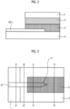
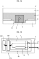
- the optical waveguide element of the present invention is an optical waveguide element including: a rib optical waveguide 10 that is made of a material (1) having an electro-optic effect; and the reinforcing substrate 2 that supports the optical waveguide, in which one end of the optical waveguide forms a tapered portion 11 of which a width narrows toward an end surface of the reinforcing substrate, a structure 3 made of a material having a higher refractive index than a material constituting the reinforcing substrate is provided so as to cover the tapered portion, and a coating layer 4 made of a material having a lower refractive index than the material constituting the structure is disposed so as to cover the structure.
- a substrate of a ferroelectric material having an electro-optic effect specifically, lithium niobate (LN), lithium tantalate (LT), lead lanthanum zirconate titanate (PLZT), or the like, an epitaxial film using these materials, or the like can be used.
- various materials, such as a semiconductor material or an organic material can also be used as a substrate of the optical waveguide element.
- the thickness of the optical waveguide 10 used in the present invention is extremely thin on the order of several pm, and there is a method of mechanically polishing and thinning a crystal substrate, such as LN, or a method of using an epitaxial film, such as LN.
- a method of mechanically polishing and thinning a crystal substrate such as LN
- a method of using an epitaxial film such as LN.
- an epitaxial film for example, an epitaxial film is formed by a sputtering method, a CVD method, a sol-gel method, or the like in accordance with the crystal orientation of a single crystal substrate, such as a SiOz substrate, a sapphire single crystal substrate, or a silicon single crystal substrate.
- the reinforcing substrate 2 is disposed on the back surface side of the optical waveguide 10 in order to enhance the mechanical strength of the optical waveguide element.
- the reinforcing substrate 2 may be made of a material having a lower refractive index than the waveguide layer, such as a SiO 2 substrate. It is also possible to directly join a layer 1 constituting the optical waveguide 10 onto the reinforcing substrate 2, or use the reinforcing substrate 2 as a base for crystal growth to provide a layer of an epitaxial film constituting the optical waveguide.
- a method for forming a rib-type protrusion constituting the optical waveguide a method of forming the protrusion by dry or wet etching a layer (for example, an LN layer) forming the optical waveguide can be used.
- a method of thermally diffusing a high refractive index material, such as Ti, to the position of the rib portion can also be used.
- the feature of the optical waveguide element of the present invention employs, as shown in FIG. 1 or 3 , the tapered portion 11 of which the width narrows toward the end surface of the reinforcing substrate 2, a so-called “reverse tapered shape" as one end (the input portion or the output portion of the light wave) of the rib optical waveguide 10.
- This shape is completely different from the tapered shape of the conventional Patent Literature Nos. 1 to 3 in which the width becomes wider or the thickness becomes thicker toward the end portion.
- the present invention is not limited to such a shape, and for example, a shape in which the thickness gradually decreases, a shape in which the width narrows and the thickness also decreases, or the like can also be employed within a range in which the refractive index difference between a core portion and a clad portion can be secured when the light wave propagates in a single mode.
- the structure 3 made of a material having a higher refractive index than the material constituting the reinforcing substrate 2 is provided so as to cover the tapered portion of which the width is narrowed down.
- the refractive index of this structure is lower than the refractive index of the material constituting the optical waveguide 10.
- the material of the structure 3 it is possible to use an inorganic material, such as glass, or a resin material with an increased refractive index. Considering the durability of the SSC, the structure 3 may be made of an inorganic material.
- the structure 3 is made of a resin material, such as an adhesive or a photoresist (permanent resist), air bubbles are likely to enter the vicinity of the optical waveguide 10 when the resin is applied. Therefore, it is more preferable to form a film of an inorganic material through a sputtering method or the like.
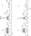
- FIGS. 4A to 4D The respective cross-sections taken along dotted lines A-A' to D-D' of FIG. 3 are shown in FIGS. 4A to 4D .
- the optical waveguide is gradually switched from FIGS. 4A to 4D to realize spot size conversion of the propagating light wave.
- a light wave propagating through the optical waveguide 10 and having an MFD of 1 um can be expanded to a light wave having an MFD of about 3 ⁇ m at the stage of FIG. 4D while maintaining the single mode.
- FIG. 6 shows a case where a resist pattern is disposed on the pattern of the optical waveguide 10 produced once and the LN around the optical waveguide 10 is further removed to make the depth of the optical waveguide 10 deeper, as shown in FIG. 5 .
- the width of the optical waveguide 12 becomes narrower. Since the width of the reverse tapered shape also sharply narrows, the propagation loss increases.
- tapered portions (11, 15) include optical waveguides (10, 14) having a shape of being stacked in multiple stages, and the width W1 of the optical waveguide 10 disposed on the upper side is narrower than the width W2 of the optical waveguide 14 disposed on the lower side.
- the first etching is performed using a resist pattern that matches the shape of the optical waveguide 10
- the second etching is performed using a resist pattern that matches the shape of the optical waveguide 14.
- the vicinity of the tapered portion is etched until the reinforcing substrate 2 is exposed, but an extremely thin LN portion may remain.
- FIGS. 8 to 11D show an SSC employing the shape of the tapered portion shown in FIG. 7 .
- LN (1) which is the material constituting the optical waveguide, may be left without particularly removing a portion 16 apart from the optical waveguide .
- the tapered portion of FIG. 8 is stacked in two stages to constitute the tapered portions (11, 15), but the present invention is not limited to the two stages, and three or more stages may be used.
- the structure 3 is disposed so as to cover the tapered portion of the optical waveguide.
- the structure 3 is similar to that described above.
- the coating layer 4 and the upper reinforcing substrate 5 are disposed in the same manner as in FIG. 2 .
- the propagation loss of the SSC having the shape of FIG. 1 and the SSC having the shape of FIG. 8 was compared by simulation.
- the refractive index of each member it is assumed that the optical waveguide 10 has a refractive index of 2.138, the reinforcing substrate 2 has a refractive index of 1.494, the structure 3 has a refractive index of 1.575, and the coating layer 4 has a refractive index of 1.542.
- the thickness of the layer 1 of the material constituting the optical waveguide of FIG. 1 is 0.2 um
- the thickness of the optical waveguide 10 protruding from the front surface of the layer 1 is 0.6 um
- the width of the optical waveguide 10 is 1.3 um.
- the width of the optical waveguide constituting the tapered portion 11 in FIG. 8 is 1.3 um and the width of the optical waveguide constituting the tapered portion 15 is 3.0 ⁇ m.
- the tapered portion formed in two stages as shown in FIG. 8 improved the propagation loss from 0.41 to 0.05 (Loss/dB) as compared with the tapered portion formed in one stage.
- the propagation loss of the light wave propagating from the optical waveguide 10 through the SSC portion to the optical fiber was improved from 0.73 to 0.32 (Loss/dB).
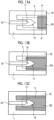
- FIGS. 12 to 13C a configuration can also be employed in which the thickness of the reinforcing substrate 20 near the end surface of the reinforcing substrate (on the lower right side in FIG. 12 ) is made equal to or thinner than the thickness of the reinforcing substrate 2 provided on the lower side of the tapered portion (15).
- FIGS. 13A to 13C show a thinned portion of the reinforcing substrate 20 (a region cut deeper in the reinforcing substrate 2) as shaded portions R1 to R3.
- the present invention is not limited to a case of thinning the reinforcing substrate 2 only near the end surface of the optical waveguide element of FIG. 13A , and a configuration can also be employed in which the reinforcing substrate 2 is thinned in conformity with the shape of the tapered portion 15 as shown in FIG. 13C .
- FIG. 14 is a cross-sectional view taken along a dotted line A-A' of FIG. 13A , and the white cross shown in FIG. 14 is displayed by being superimposed on the tip position of the tapered portion 11 of the optical waveguide.
- the reinforcing substrate 2 is made thinner, it is also possible to adjust the position of the tapered portion 11, which is the tip of the optical waveguide 10, to the central position of the optical waveguide having the structure 3 as the core portion, and it is possible to reduce the propagation loss.
- the MFD of the light wave propagating through the optical waveguide in the element is lower than 3 um (for example, about 1 um), and the mode field diameter of the optical fiber that is connected to the optical waveguide element and through which the light wave is input to or output from the optical waveguide in the element is 3 um or higher (for example, 10 um) .
- the radius of curvature of the optical waveguide in the optical waveguide element can be reduced while using a general optical fiber, which contributes to miniaturization of the optical waveguide element.
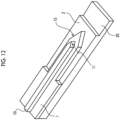
- the optical waveguide element of the present invention is provided with a modulation electrode that modulates the light wave propagating through the optical waveguide 10, and is accommodated in a case 8 as shown in FIG. 15 . Further, an optical fiber F through which a light wave is input to and output from the optical waveguide is provided, so that an optical modulation device MD can be configured.
- the optical fiber is introduced into the case via a through-hole penetrating the side wall of the case and directly joined to the optical waveguide element.
- the optical waveguide element and the optical fiber can also be optically connected via a space optical system.
Landscapes
- Physics & Mathematics (AREA)
- General Physics & Mathematics (AREA)
- Optics & Photonics (AREA)
- Engineering & Computer Science (AREA)
- Nonlinear Science (AREA)
- Microelectronics & Electronic Packaging (AREA)
- Power Engineering (AREA)
- Optical Integrated Circuits (AREA)
- Optical Modulation, Optical Deflection, Nonlinear Optics, Optical Demodulation, Optical Logic Elements (AREA)
- Optical Couplings Of Light Guides (AREA)
Applications Claiming Priority (2)
| Application Number | Priority Date | Filing Date | Title |
|---|---|---|---|
| JP2020165003A JP7528691B2 (ja) | 2020-09-30 | 2020-09-30 | 光導波路素子及びそれを用いた光変調デバイス並びに光送信装置 |
| PCT/JP2021/035807 WO2022071377A1 (ja) | 2020-09-30 | 2021-09-29 | 光導波路素子及びそれを用いた光変調デバイス並びに光送信装置 |
Publications (2)
| Publication Number | Publication Date |
|---|---|
| EP4224247A1 true EP4224247A1 (de) | 2023-08-09 |
| EP4224247A4 EP4224247A4 (de) | 2024-11-13 |
Family
ID=80950606
Family Applications (1)
| Application Number | Title | Priority Date | Filing Date |
|---|---|---|---|
| EP21875677.3A Pending EP4224247A4 (de) | 2020-09-30 | 2021-09-29 | Optisches wellenleiterelement und optische modulationsvorrichtung und optische übertragungsvorrichtung damit |
Country Status (5)
| Country | Link |
|---|---|
| US (1) | US12422628B2 (de) |
| EP (1) | EP4224247A4 (de) |
| JP (1) | JP7528691B2 (de) |
| CN (1) | CN116134352A (de) |
| WO (1) | WO2022071377A1 (de) |
Families Citing this family (5)
| Publication number | Priority date | Publication date | Assignee | Title |
|---|---|---|---|---|
| JP2024107830A (ja) * | 2023-01-30 | 2024-08-09 | 住友大阪セメント株式会社 | 光導波路素子及びそれを用いた光変調デバイス並びに光送信装置 |
| CN116360033A (zh) * | 2023-03-15 | 2023-06-30 | 浙江大学绍兴研究院 | 一种基于玻璃基板的单模光纤与锆钛酸铅波导的耦合方式 |
| US20250035838A1 (en) * | 2023-07-27 | 2025-01-30 | Intel Corporation | Low loss splitter-combiner waveguide structures in photonic circuits |
| WO2025027739A1 (en) * | 2023-07-31 | 2025-02-06 | Nippon Telegraph And Telephone Corporation | Spot size converter and optical integrated device |
| CN121420224A (zh) * | 2024-03-26 | 2026-01-27 | 住友大阪水泥股份有限公司 | 光波导元件、光调制器和光发送装置 |
Family Cites Families (31)
| Publication number | Priority date | Publication date | Assignee | Title |
|---|---|---|---|---|
| JP3178565B2 (ja) * | 1993-06-30 | 2001-06-18 | 日本電信電話株式会社 | 半導体光デバイス |
| TW479387B (en) * | 1999-11-23 | 2002-03-11 | Nanovation Tech Inc | Optical waveguide having a weakly-confining waveguide section and a strongly-confining waveguide section ooptically coupled by a tapered neck |
| JP3923355B2 (ja) * | 2002-04-19 | 2007-05-30 | 日本電信電話株式会社 | 光変調装置 |
| JP2004133446A (ja) * | 2002-09-20 | 2004-04-30 | Nippon Telegr & Teleph Corp <Ntt> | 光モジュール及び製造方法 |
| JP4146788B2 (ja) * | 2003-12-10 | 2008-09-10 | 日本電信電話株式会社 | 光導波路接続モジュールおよびその導波路作製方法 |
| JP4265439B2 (ja) * | 2004-02-24 | 2009-05-20 | パナソニック電工株式会社 | 光導波路モジュールの製造方法 |
| JP2005266381A (ja) * | 2004-03-19 | 2005-09-29 | Nec Corp | 導波路型光スプリッタ及びこれを備えた導波路型光モジュール |
| JP4868763B2 (ja) | 2005-03-31 | 2012-02-01 | 住友大阪セメント株式会社 | 光変調器 |
| US7643710B1 (en) * | 2008-09-17 | 2010-01-05 | Intel Corporation | Method and apparatus for efficient coupling between silicon photonic chip and optical fiber |
| JP2010230741A (ja) * | 2009-03-26 | 2010-10-14 | Ngk Insulators Ltd | 光変調器 |
| JP2010237592A (ja) * | 2009-03-31 | 2010-10-21 | Sumitomo Osaka Cement Co Ltd | 光素子と光ファイバとの接合構造 |
| WO2012042708A1 (ja) | 2010-09-28 | 2012-04-05 | 日本電気株式会社 | 光導波路構造及び光導波路デバイス |
| WO2013146818A1 (ja) | 2012-03-28 | 2013-10-03 | 日本電気株式会社 | 光導波路構造及び光導波路デバイス |
| FR3017216B1 (fr) * | 2014-01-31 | 2017-05-26 | Univ De Franche-Comte | Methode de fabrication d'un guide d'onde optique a structure "ridge" a faibles pertes de couplage entre le guide d'onde optique a structure "ridge" et une fibre optique, et guide d'onde optique a structure "ridge" fabrique par cette methode |
| JP6369036B2 (ja) | 2014-02-04 | 2018-08-08 | 日本電気株式会社 | 光導波路及び光導波路の製造方法 |
| US10663663B2 (en) * | 2014-02-28 | 2020-05-26 | Ciena Corporation | Spot-size converter for optical mode conversion and coupling between two waveguides |
| JP6335609B2 (ja) * | 2014-04-23 | 2018-05-30 | 三菱電機株式会社 | スポットサイズ変換素子および半導体装置 |
| JP6398551B2 (ja) * | 2014-09-30 | 2018-10-03 | 住友大阪セメント株式会社 | 光変調器 |
| JP6394285B2 (ja) * | 2014-10-31 | 2018-09-26 | 富士通株式会社 | 光導波路、スポットサイズ変換器及び光装置 |
| US9547129B1 (en) * | 2015-01-21 | 2017-01-17 | Inphi Corporation | Fiber coupler for silicon photonics |
| US9575251B1 (en) * | 2015-08-11 | 2017-02-21 | Oracle International Corporation | Optical mode converter having multiple regions |
| EP3514588A1 (de) * | 2018-01-18 | 2019-07-24 | Huawei Technologies Co., Ltd. | Optischer chip mit einem kantenkoppler |
| GB201803170D0 (en) * | 2018-02-27 | 2018-04-11 | Optoscribe Ltd | Optical apparatus and methods of manufacture thereof |
| JP7073963B2 (ja) * | 2018-07-24 | 2022-05-24 | 住友大阪セメント株式会社 | 光導波路素子 |
| JP2020091378A (ja) * | 2018-12-05 | 2020-06-11 | 住友大阪セメント株式会社 | 光変調器 |
| FR3098312B1 (fr) * | 2019-07-05 | 2023-01-06 | Almae Tech | composant semi-conducteur actif, composant passif à base de silicium, assemblage desdits composants et procédé de couplage entre guides d’ondes |
| CN110632702B (zh) * | 2019-10-23 | 2021-04-09 | 北京工业大学 | 一种lnoi基光波导反向楔形模斑耦合器及制备方法 |
| CN111175999B (zh) * | 2020-02-24 | 2021-05-04 | 上海交通大学 | 基于铌酸锂-硅晶圆的高速低电压电光调制器 |
| JP7371556B2 (ja) * | 2020-03-31 | 2023-10-31 | 住友大阪セメント株式会社 | 光導波路素子 |
| CN111458793A (zh) * | 2020-04-17 | 2020-07-28 | 中国科学院半导体研究所 | Lnoi基脊型光波导端面耦合结构及其应用 |
| JP7666070B2 (ja) * | 2021-03-30 | 2025-04-22 | 住友大阪セメント株式会社 | 光導波路素子及びそれを用いた光変調デバイス並びに光送信装置 |
-
2020
- 2020-09-30 JP JP2020165003A patent/JP7528691B2/ja active Active
-
2021
- 2021-09-29 CN CN202180063004.2A patent/CN116134352A/zh active Pending
- 2021-09-29 EP EP21875677.3A patent/EP4224247A4/de active Pending
- 2021-09-29 WO PCT/JP2021/035807 patent/WO2022071377A1/ja not_active Ceased
- 2021-09-29 US US18/029,393 patent/US12422628B2/en active Active
Also Published As
| Publication number | Publication date |
|---|---|
| JP2022056980A (ja) | 2022-04-11 |
| EP4224247A4 (de) | 2024-11-13 |
| WO2022071377A1 (ja) | 2022-04-07 |
| US20230314732A1 (en) | 2023-10-05 |
| US12422628B2 (en) | 2025-09-23 |
| JP7528691B2 (ja) | 2024-08-06 |
| CN116134352A (zh) | 2023-05-16 |
Similar Documents
| Publication | Publication Date | Title |
|---|---|---|
| US12422628B2 (en) | Optical waveguide element, and optical modulation device and optical transmission apparatus using same | |
| US7054512B2 (en) | Optical waveguide, optical device, and method of manufacturing optical waveguide | |
| EP3889655B1 (de) | Lichtwellenleitervorrichtung | |
| EP3978993A1 (de) | Optisches wellenleiterelement, optische modulationsvorrichtung und optische übertragungsvorrichtung mit einem optischen wellenleiterelement | |
| JP7666070B2 (ja) | 光導波路素子及びそれを用いた光変調デバイス並びに光送信装置 | |
| US12197052B2 (en) | Optical waveguide element | |
| US12461306B2 (en) | Optical waveguide element, optical modulation device using optical waveguide element, and optical transmission device using optical waveguide element | |
| CN118732154A (zh) | 光波导元件、使用光波导元件的光调制器件及光发送装置 | |
| US20240310663A1 (en) | Optical waveguide element, optical modulation device using the same, and optical transmitter | |
| WO2023188311A1 (ja) | 光導波路素子及びそれを用いた光変調デバイス並びに光送信装置 | |
| US12607803B2 (en) | Optical waveguide element, and optical transmission apparatus and optical modulation device using same | |
| JP7670153B2 (ja) | 光導波路素子及びそれを用いた光変調デバイス並びに光送信装置 | |
| CN121420224A (zh) | 光波导元件、光调制器和光发送装置 | |
| EP4343395A1 (de) | Optisches wellenleiterelement und optische übertragungsvorrichtung und optische modulationsvorrichtung damit | |
| CN118409391A (zh) | 光波导元件、使用光波导元件的光调制器件及光发送装置 | |
| WO2023243014A1 (ja) | 光導波路接続構造 |
Legal Events
| Date | Code | Title | Description |
|---|---|---|---|
| STAA | Information on the status of an ep patent application or granted ep patent |
Free format text: STATUS: THE INTERNATIONAL PUBLICATION HAS BEEN MADE |
|
| PUAI | Public reference made under article 153(3) epc to a published international application that has entered the european phase |
Free format text: ORIGINAL CODE: 0009012 |
|
| STAA | Information on the status of an ep patent application or granted ep patent |
Free format text: STATUS: REQUEST FOR EXAMINATION WAS MADE |
|
| 17P | Request for examination filed |
Effective date: 20230329 |
|
| AK | Designated contracting states |
Kind code of ref document: A1 Designated state(s): AL AT BE BG CH CY CZ DE DK EE ES FI FR GB GR HR HU IE IS IT LI LT LU LV MC MK MT NL NO PL PT RO RS SE SI SK SM TR |
|
| DAV | Request for validation of the european patent (deleted) | ||
| DAX | Request for extension of the european patent (deleted) | ||
| A4 | Supplementary search report drawn up and despatched |
Effective date: 20241011 |
|
| RIC1 | Information provided on ipc code assigned before grant |
Ipc: G02F 1/035 20060101ALI20241007BHEP Ipc: G02B 6/122 20060101ALI20241007BHEP Ipc: G02F 1/01 20060101AFI20241007BHEP |