EP4227736A1 - Film transmettant les rayons euv - Google Patents
Film transmettant les rayons euv Download PDFInfo
- Publication number
- EP4227736A1 EP4227736A1 EP22883267.1A EP22883267A EP4227736A1 EP 4227736 A1 EP4227736 A1 EP 4227736A1 EP 22883267 A EP22883267 A EP 22883267A EP 4227736 A1 EP4227736 A1 EP 4227736A1
- Authority
- EP
- European Patent Office
- Prior art keywords
- euv
- membrane
- layer
- main layer
- transmittance
- Prior art date
- Legal status (The legal status is an assumption and is not a legal conclusion. Google has not performed a legal analysis and makes no representation as to the accuracy of the status listed.)
- Pending
Links
Images


Classifications
-
- G—PHYSICS
- G03—PHOTOGRAPHY; CINEMATOGRAPHY; ANALOGOUS TECHNIQUES USING WAVES OTHER THAN OPTICAL WAVES; ELECTROGRAPHY; HOLOGRAPHY
- G03F—PHOTOMECHANICAL PRODUCTION OF TEXTURED OR PATTERNED SURFACES, e.g. FOR PRINTING, FOR PROCESSING OF SEMICONDUCTOR DEVICES; MATERIALS THEREFOR; ORIGINALS THEREFOR; APPARATUS SPECIALLY ADAPTED THEREFOR
- G03F1/00—Originals for photomechanical production of textured or patterned surfaces, e.g., masks, photo-masks, reticles; Mask blanks or pellicles therefor; Containers specially adapted therefor; Preparation thereof
- G03F1/22—Masks or mask blanks for imaging by radiation of 100nm or shorter wavelength, e.g. X-ray masks, extreme ultraviolet [EUV] masks; Preparation thereof
-
- G—PHYSICS
- G03—PHOTOGRAPHY; CINEMATOGRAPHY; ANALOGOUS TECHNIQUES USING WAVES OTHER THAN OPTICAL WAVES; ELECTROGRAPHY; HOLOGRAPHY
- G03F—PHOTOMECHANICAL PRODUCTION OF TEXTURED OR PATTERNED SURFACES, e.g. FOR PRINTING, FOR PROCESSING OF SEMICONDUCTOR DEVICES; MATERIALS THEREFOR; ORIGINALS THEREFOR; APPARATUS SPECIALLY ADAPTED THEREFOR
- G03F1/00—Originals for photomechanical production of textured or patterned surfaces, e.g., masks, photo-masks, reticles; Mask blanks or pellicles therefor; Containers specially adapted therefor; Preparation thereof
- G03F1/62—Pellicles, e.g. pellicle assemblies, e.g. having membrane on support frame; Preparation thereof
-
- G—PHYSICS
- G02—OPTICS
- G02B—OPTICAL ELEMENTS, SYSTEMS OR APPARATUS
- G02B1/00—Optical elements characterised by the material of which they are made; Optical coatings for optical elements
- G02B1/10—Optical coatings produced by application to, or surface treatment of, optical elements
- G02B1/14—Protective coatings, e.g. hard coatings
Definitions
- the present invention relates to an EUV transmissive membrane.
- EUV extreme ultraviolet
- ArF ArF
- the wavelength was reduced to 1/10 or less at once, and optical properties thereof were completely different.
- pellicle which serves as a particle adhesion-preventing membrane of, for example, a photomask (reticle). For this reason, device manufacturers currently cannot use pellicles when manufacturing semiconductor devices.
- Patent Literature 1 JP6858817B discloses a pellicle membrane including a core layer that contains a material substantially transparent for EUV radiation such as (poly-)Si and a cap layer that contains a material absorbing IR radiation.
- CNT carbon nanotube
- Patent Literature 3 JP2017-522590A discloses a membrane that is transmissive to EUV radiation with high and low-doped regions, which is expected to improve temperature characteristics of the membrane.
- Patent Literature 1 JP6858817B discloses a pellicle membrane for a lithography apparatus including a main layer and a protective layer for improving IR emissivity and particularly describes a metal such as Pd or Ag as the protective layer in a case where the main layer is Si.
- a pellicle membrane has been proposed that dissipates heat by IR radiation from the protective layer rather than the main layer.
- a metal such as Pd or Ag, which is considered a protective layer having high IR emissivity, has low EUV transmittance and thus does not provide a pellicle membrane having both practical EUV transmittance and high IR emissivity.
- IR light is mainly emitted among rays having various wavelengths. This is because the wavelength of a ray emitted from an object is determined by the temperature of the object. In fact, when the pellicle membrane is heated to a temperature of about 500 to 800°C during exposure, a ray having a wavelength of 1 to 2 ⁇ m is most emitted in this temperature range. Accordingly, there is a demand for a pellicle membrane having not only high EUV transmittance but also high emissivity of IR light having a wavelength of about 2 ⁇ m.
- the inventors have recently found that by combining a main layer having high IR emissivity and a protective layer having high IR transmittance to constitute an EUV transmissive membrane having an EUV transmittance of 80.0% or more, it is possible to provide an EUV transmissive membrane having not only high EUV transmittance but also high IR emissivity.
- an object of the present invention is to provide an EUV transmissive membrane having not only high EUV transmittance but also high IR emissivity.
- the present invention provides the following aspects:
- the EUV transmissive membrane according to Aspect 5 wherein a constituent element of the additive has an electronegativity that is 0.3 or higher or 0.3 or lower than the electronegativity of a major constituent element of the main layer.
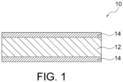
- FIG. 1 illustrates a schematic cross-sectional view of an EUV transmissive membrane 10 according to an embodiment of the present invention.
- An EUV transmissive membrane 10 has an EUV transmittance of 80.0% or more at a wavelength of 13.5 nm.
- the EUV transmissive membrane 10 includes a main layer 12 and a protective layer 14 that covers at least one side of the main layer.
- the main layer 12 has an IR emissivity of 2.0% or more at a wavelength of 2 ⁇ m, while the protective layer 14 has an IR transmittance of 70% or more at a wavelength of 2 ⁇ m.
- an EUV transmissive membrane having an EUV transmittance of 80.0% or more By combining a main layer having high IR emissivity and a protective layer having high IR transmittance with respect to IR light at a wavelength of 2 ⁇ m to constitute an EUV transmissive membrane having an EUV transmittance of 80.0% or more, it is possible to provide an EUV transmissive membrane having not only high EUV transmittance but also high IR emissivity.
- the pellicle membrane has high transmittance to EUV light but slightly absorbs EUV light. Even though the amount of EUV light absorbed is small, the pellicle membrane generates heat due to continuous irradiation of high-energy EUV light during exposure. At this time, even if the temperature of the pellicle membrane rises, the temperature of a pellicle frame rises only slightly through thermal conduction. Thus, although the pellicle membrane expands, the pellicle frame does not expand so much, causing wrinkles in the pellicle.
- Patent Literature 1 JP6858817B discloses a pellicle membrane for a lithography apparatus including a main layer and a protective layer for improving IR emissivity and particularly describes a metal such as Pd or Ag as the protective layer in a case where the main layer is Si.
- a pellicle membrane has been proposed that dissipates heat by IR radiation from the protective layer rather than the main layer.
- Pd and Ag which are considered as protective layers having high IR emissivity, have low EUV transmittance and thus do not provide a pellicle membrane having both practical EUV transmittance and high IR emissivity. All these problems are successfully solved by the EUV transmissive membrane 10 of the present invention.
- the EUV transmissive membrane 10 of the present invention can dissipate heat generated by the absorption of the EUV light by the IR radiation from the main layer while increasing the EUV transmittance of the EUV transmissive membrane 10 by combining a main layer having both high EUV transmittance and high IR emissivity (e.g., a layer composed of metal) and a protective layer having both high EUV transmittance and high IR transmittance (e.g., a layer composed of a nonmetal).
- a main layer having both high EUV transmittance and high IR emissivity e.g., a layer composed of metal
- a protective layer having both high EUV transmittance and high IR transmittance e.g., a layer composed of a nonmetal
- the IR light is emitted from the main layer 12, and the protective layer 14 transmits the IR light emitted from the main layer 12, thereby emitting the IR light to the outside of the EUV transmissive membrane 10 to dissipate the heat. Therefore, the temperature rise of the EUV transmissive membrane 10 is suppressed.
- transmittance + reflectance + absorptivity 1
- the above relational equation is satisfied for a specific wavelength, and it is possible to have an EUV transmittance of 0.95 or more at a wavelength of 13.5 nm and an emissivity of 0.1 for the main ray (IR ray at a wavelength of 2 ⁇ m) of the heat dissipation by radiation.
- the EUV transmissive membrane 10 has an EUV transmittance of 80.0% or more, preferably 85.0% or more, more preferably 90.0% or more, and even more preferably 93.0% or more at a wavelength of 13.5 nm. Since a higher EUV transmittance is desirable, the upper limit is not particularly limited. Although the upper limit is ideally 100%, the EUV transmissive membrane 10 can typically have a EUV transmittance of 99% or less, more typically 98% or less, and even more typically 95% or less.
- the main layer 12 has an IR emissivity of 2.0% or more, preferably 2.5% or more, more preferably 5.0% or more, even more preferably 8.0% or more, particularly preferably 13.0% or more, and most preferably 15.0% or more at a wavelength of 2 ⁇ m. Since a higher IR emissivity is desirable, the upper limit is not particularly limited, but the main layer 12 can typically have an IR emissivity of 30.0% or less, more typically 27.5% or less, and even more typically 25.0% or less.
- the main layer 12 preferably contains at least one selected from the group consisting of Be, Si, and B 4 C as a main component, more preferably contains Be or Si as a main component, and even more preferably contains Be as a main component.
- the main layer 12 may contain a ceramic material having a low electrical resistance equivalent to that of a metal such as B 4 C, in addition to a metal material having a particularly high EUV transmittance, such as Be or Si.
- the "main component" in the main layer 12 means a component that accounts for 98.0% by weight or more, preferably 99.0% by weight or more, and more preferably 99.5% by weight or more of the main layer 12.
- the main layer 12 may be composed of at least one selected from the group consisting of Be, Si, and B 4 C.
- the main layer can be made to have high EUV transmittance and high IR emissivity more effectively while ensuring basic functions as a pellicle membrane (such as particle adhesion preventing function).
- the thickness of the main layer 12 is preferably 10 to 70 nm, more preferably 15 to 50 nm, and even more preferably 20 to 35 nm.
- the thickness of the main layer 12 is preferably 5 nm or more given maintaining a mechanical strength sufficient for practical use.
- the thickness of the main layer 12 is preferably 50 nm or less, more preferably 40 nm or less, and even more preferably 30 nm or less.
- the protective layer 14 is a layer for protecting the main layer 12. Accordingly, the protective layer 14 covers at least one side of the main layer 12, and it is preferable to cover both sides of the main layer 12 with a pair of the protective layer 14.
- the protective layer 14 has an IR transmittance of 70% or more, preferably 75% or more, more preferably 78% or more, and even more preferably 80% or more at a wavelength of 2 ⁇ m. Since a higher IR transmittance is desirable, the upper limit is not particularly limited, but the protective layer 14 can typically have an IR transmittance of 90% or less, more typically 87% or less, and even more typically 85% or less.
- the protective layer 14 is a layer for protecting the main layer 12 in the fabrication process of the EUV transmissive membrane 10 as described above, and is formed for the purpose of preventing oxidation of the main layer 12 and preventing reaction (e.g., oxidation or corrosion) with chemicals in the process.
- the protective layer 14 has high transmittance to IR light in order not to disturb IR radiation from the main layer 12.
- the protective layer 14 also has high EUV transmittance.
- the protective layer 14 is preferably composed of at least one selected from the group consisting of calcium fluoride, silicon dioxide, and beryllium nitride, more preferably composed of silicon dioxide or beryllium nitride, and even more preferably composed of beryllium nitride.
- the protective layer 14 does not need to be composed only of these compounds as long as 99% by weight or more, preferably 99.5% by weight or more, and even more preferably 99.8% by weight or more of the protective layer 14 may be composed of these compounds.
- beryllium nitride as used herein means a comprehensive composition that allows not only a stoichiometric composition such as Be 3 N 2 but also a non-stoichiometric composition such as Be 3 N 2-x , wherein 0 ⁇ x ⁇ 2. The same is also applicable to other compound names such as calcium fluoride and silicon dioxide.
- the protective layer 14 preferably has a thickness of 5 nm or less, and more preferably 3 nm or less.
- the lower limit of the thickness of the protective layer 14 is not particularly limited, but is typically 0.3 nm or more, and more typically 0.5 or more.
- the thickness of the protective layer 14 is 5 nm or less, the EUV transmittance can be increased, and when the thickness of the protective layer 14 is 0.3 nm or more, basic functions as a protective layer such as an antioxidation function can be maintained.
- the main layer 12 preferably contains at least one selected from the group consisting of Be, Si, and B 4 C as the main component, while the protective layer 14 is preferably composed of at least one selected from the group consisting of calcium fluoride, silicon dioxide, and beryllium nitride.
- the main layer 12 is preferably composed of a metal or a semimetal (particularly, a metal), and the protective layer 14 is preferably composed of a nonmetal.
- both the main layer 12 and the protective layer 14 exhibit high EUV transmittance, preferably, by combining the main layer 12 composed of a non-dielectric which is a metal having high EUV transmittance, and the protective layer 14 composed of a dielectric which is a nonmetal having high EUV transmittance while the main layer 12 has high IR emissivity and the protective layer 14 has low IR emissivity.
- the IR radiation emitted from the main layer 12 is transmitted without being absorbed by the protective layer 14 and emitted from the EUV transmissive membrane 10.
- the EUV transmissive membrane can be more effectively made to have not only high EUV transmittance but also high IR emissivity.
- the main layer 12 contains Be as a main component is considered. Since beryllium is a metal, the thinner it is, the higher the IR emissivity.
- the IR emissivity of Be at various thicknesses was calculated using optical theory and found to be 2.1% at a thickness of 100 nm, 2.9% at 50 nm, 4.4% at 30 nm, and 6.2% at 20 nm. In this calculation, the Be layer is assumed to be in an ideal specular state, and the IR reflectance in this case is assumed to be higher than the IR reflectance of the actual Be layer. For this reason, the IR emissivity of the Be layer in the optical theory calculation is calculated to be lower than the IR emissivity of the actual Be layer.
- the actual Be layer has higher IR emissivity than the above calculation results.
- theoretical calculations show that the EUV transmittance of the Be layer is 86.7% at a thickness of 100 nm. 93.1% at 50 nm, 95.8% at 30 nm, and 97.2% at 20 nm.
- the thinner the main layer 12 containing Be as a main component the higher the EUV transmittance and the higher the IR emissivity.
- the main layer 12 preferably contains an additive. This can further increase the IR emissivity of the main layer 12.
- the IR emissivity of the main layer 12 is considered to be higher because the additive becomes a scattering source of conduction electrons.
- the EUV transmittance of the additive itself is low, the EUV transmittance of the main layer 12 will also decrease, and thus it is preferable to select an additive having high EUV transmittance.
- the constituent elements of the additive preferably have an electronegativity that is 0.3 or higher or 0.3 or lower, more preferably 0.33 or higher or 0.33 or lower, and even more preferably 0.35 or higher or 0.35 or lower than the electronegativity of the major constituent element of the main layer 12.
- the upper limit of the difference between the electronegativity of the constituent element of the additive and the electronegativity of the major constituent element of the main layer 12 is not particularly limited, but typically is 1.2 or less, and more typically 1.0 or less.
- the greater the difference between the electronegativity of the main component (e.g., Be) of the main layer 12 and the electronegativity of the additive the greater the scattering power of the conduction electrons.
- the "major constituent element" of the main layer 12 as used herein means an element most abundantly contained in the main layer 12.
- the major constituent element is Be.
- the additive preferably contains at least one element selected from the group consisting of rubidium (Rb), strontium (Sr), yttrium (Y), niobium (Nb), molybdenum (Mo), silicon (Si), potassium (K), calcium (Ca), boron (B), and carbon (C).
- the content of the additive is preferably 5 to 40 at%, more preferably 10 to 35 at%, and even more preferably 15 to 30 at% with respect to the Be content in the main layer 12.
- the content of the additive is preferably 5 to 40 at% with respect to the content of Si in the main layer 12, although the effect depends on the component of the additive.
- the content of the additive is more than 5 at%, the above-described advantages of the additive can be effectively realized.
- the content of the additive is less than 40 at%, the mechanical strength of the EUV transmissive membrane 10 can be maintained to make it less likely to be damaged, and the EUV transmittance of the main layer 12 can be increased.
- the content of these additives can be determined, for example, by cutting EUV transmissive membranes into cross sections by focused ion beam (FIB) processing to prepare samples, observing the samples with a transmission electron microscope (TEM) (JME-2100F, manufactured by JEOL Ltd.) at 200 kV, and analyzing elements with an EDS analyzer (JED-2300T, manufactured by JEOL Ltd.) at an acceleration voltage of 5 keV for elemental mapping and point analysis mode.
- TEM transmission electron microscope
- JED-2300T manufactured by JEOL Ltd.
- the protective layer 14 preferably has a nitrogen concentration gradient region where nitrogen concentration decreases as closer to the main layer 12.
- the composition of beryllium nitride may include from the stoichiometric composition such as Be 3 N 2 to the non-stoichiometric composition such as Be 3 N 2-x , wherein 0 ⁇ x ⁇ 2, as described above, the beryllium nitride constituting the protective layer 14 preferably has a gradient composition that is richer in beryllium as closer to the main layer 12.
- the thickness of the nitrogen concentration gradient region is preferably smaller than that of the protective layer 14. In other words, the entire thickness of the protective layer 14 does not need to be in the nitrogen concentration gradient region. For example, it is preferable that only a part of the thickness of the protective layer 14, for example, a region of preferably 10 to 70% and more preferably 15 to 50% of the thickness of the protective layer 14 is the nitrogen concentration gradient region.
- the main region for transmitting EUV is preferably in a form of the free-standing membrane.
- the substrate e.g., Si substrate
- the main region preferably consists of the main layer 12 and the protective layer 14.
- the EUV transmissive membrane according to the present invention can be fabricated by removing an unnecessary portion of the Si substrate through etching to form a free-standing membrane. Accordingly, the main portion of the EUV transmissive membrane is in the form of the free-standing membrane in which no Si substrate remains as described above.
- a Si substrate for forming a laminated membrane thereon is prepared.
- the main region i.e., a region to be a free-standing membrane
- the Si substrate is etched by wet etching to reduce the thickness of the main region of the Si substrate to a predetermined thickness.
- the wet-etched Si substrate is cleaned and dried to prepare a Si substrate having a cavity formed by wet etching.
- the wet etching mask may be made of any material that is corrosion resistance to Si wet etchant, for example, SiOz is suitable for use.
- the wet etchant is not particularly limited as long as it is capable of etching Si.
- TMAH tetramethylammonium hydroxide
- TMAH tetramethylammonium hydroxide
- the laminated membrane may be formed by any deposition method.
- An example of the preferred deposition method is the sputtering method.
- the beryllium membrane as the main layer 12 is fabricated by sputtering using a pure Be target and the beryllium nitride membrane as the protective layer 14 is done by reactive sputtering.
- the reactive sputtering can be performed, for example, by adding nitrogen gas to the chamber during sputtering using a pure Be target, whereby beryllium and nitrogen react to each other to generate beryllium nitride.
- beryllium nitride can be produced by forming a beryllium membrane and then irradiating the membrane with nitrogen plasma to cause a nitriding reaction of beryllium, thereby generating beryllium nitride.
- synthetic methods for beryllium nitride are not limited thereto.
- it is preferable to use different beryllium targets for forming the beryllium nitride membrane and the beryllium membrane it is also possible to use the same target for forming the beryllium nitride membrane and the beryllium membrane.
- the beryllium nitride and beryllium membranes may be formed in a one-chamber sputtering apparatus as in Examples described later, or a two-chamber sputtering apparatus may be used to form the beryllium nitride and beryllium membranes in separate chambers.
- the introduction of nitrogen gas may be stopped and switched to metallic beryllium deposition while continuing a sputtering. In this way, a region is formed in which the nitrogen concentration in the film-deposited membrane decreases in the thickness direction as the concentration of nitrogen gas decreases.
- the nitrogen concentration gradient region can be formed by starting the introduction of nitrogen gas in the middle of the process while sputtering is performed, contrary to the above. The thickness of the nitrogen concentration gradient region can be controlled by adjusting the time for which the nitrogen gas concentration is changed.
- the method of adding is not particularly limited as long as the additive is mixed in the main layer at a uniform concentration.
- the method of adding the additive to the main layer include:
- Etching of Si may be performed by any method, but etching with XeF 2 is preferred.
- a composite free-standing membrane (EUV transmissive membrane) with a three-layer structure of beryllium nitride/beryllium/beryllium nitride was fabricated as follows.
- a Si wafer 20 having a diameter of 8 inches (20.32 cm) was prepared ( Figure 2A (a) ).
- a SiOz membrane 22 having a thickness of 50 nm was formed on both sides of the Si wafer 20 by thermal oxidation ( Figure 2A (b) ).
- Resist was applied to both sides of the Si wafer 20, and a resist mask 24 for SiOz etching was formed by exposure and development so that a 110 mm ⁇ 145 mm resist hole was created on one side ( Figure 2A(c) ).
- An exposed portion of the SiOz membrane 22 was etched and removed by wet-etching one side of the substrate with hydrofluoric acid to fabricate a SiOz mask 22a ( Figure 2A(d) ).
- the resist mask 24 for SiOz etching was removed with an ashing apparatus ( Figure 2A(e) ). Si was then etched with a TMAH solution. This etching was performed only for an etching time to obtain a target Si substrate having thickness of 50 ⁇ m with an etching rate measured in advance ( Figure 2A(f) ). Finally, the SiOz membrane 22 formed on the surface not subjected to Si etching was removed and cleaned with hydrofluoric acid to prepare a Si substrate 28 ( Figure 2B(g) ). The Si substrate outline may be diced with a laser 30, if necessary ( Figure 2B (h) ), to achieve the desired shape ( Figure 2B (i) ). In this way, a 110 mm ⁇ 145 mm cavity 26 was provided at the center of the 8-inch (20.32 cm) Si wafer 20 to prepare the Si substrate 28 having a Si thickness of 50 ⁇ m in the cavity 26 portion.
- a composite membrane with a three-layer structure of beryllium nitride/beryllium/beryllium nitride was formed as follows ( Figure 2B(i) ).
- the Si substrate 28 was set in a sputtering apparatus, and a pure Be target was attached thereto.
- a chamber was evacuated, the flow ratio of argon gas and nitrogen gas was adjusted to 1:1 to carry out reactive sputtering at an internal pressure of 0.5 Pa, and the reactive sputtering was terminated at the time when 2 nm of beryllium nitride was film-deposited.
- the Si substrate 28 with the composite membrane prepared in (2) above was set in a chamber of an XeF 2 etcher capable of processing an 8-inch (20.32 cm) substrate.
- the chamber was sufficiently evacuated. At this time, if moisture remains in the chamber, the moisture reacts with the XeF 2 gas to generate hydrofluoric acid, and corrosion of the etcher or unexpected etching occurs. Therefore, the sufficient evacuation was performed. If necessary, vacuuming and nitrogen gas introduction were repeated in the chamber to reduce residual moisture in the chamber. When the sufficient evacuation was achieved, a valve between a XeF 2 material tank and a preliminary space was opened. As a result, XeF 2 was sublimated, and XeF 2 gas was also accumulated in the preliminary space.
- the valve between the preliminary space and the chamber was opened to introduce the XeF 2 gas into the chamber.
- the XeF 2 gas was decomposed into Xe and F, and F reacted with Si to generate SiF 4 . Since the boiling point of SiF 4 was -95°C, SiF 4 generated was rapidly evaporated, causing a reaction of F with the newly exposed Si substrate.
- the Si etching proceeded and F in the chamber decreased, the chamber was evacuated, and the XeF 2 gas was introduced into the chamber again to perform the etching.
- the IR characteristics of the protective layer material were determined by film-depositing only the protective layer material on a calcium fluoride substrate having known IR characteristics by employing the same process as in (2) above, then performing measurement, and subtracting the influence (IR characteristics) of the calcium fluoride substrate from the obtained data.
- the IR characteristics of the main layer material were determined in the same manner as in the method used to determine the IR characteristics of the protective layer material. In this way, the IR emissivity at a wavelength of 2 ⁇ m in the main layer and the IR transmittance at a wavelength of 2 ⁇ m in the protective layer were determined. The results were as shown in Table 1.
- EUV light having a wavelength of 13.5 nm was irradiated onto the obtained EUV transmissive membrane to measure the amount of transmitted EUV light with a sensor.
- the EUV transmittance was determined by comparing the obtained measurement value with a value obtained by directly measuring the amount of EUV light with a sensor without using the EUV transmissive membrane. The results were as shown in Table 1.
- a composite free-standing membrane was fabricated and evaluated in the same manner as in Example 1, except that the main layer contained Si as an additive by forming the composite membrane as follows. The results were as shown in Table 1.
- a composite membrane with a three-layer structure of beryllium nitride/Si-containing beryllium/beryllium nitride was formed as follows ( Figure 2B(i) ).
- the Si substrate 28 was set in a multi-target sputtering apparatus, and a pure Be target and a Si target were attached thereto.
- a chamber was evacuated, the flow ratio of argon gas and nitrogen gas was adjusted to 1:1 to carry out reactive sputtering using the Be target at an internal pressure of 0.5 Pa, and the reactive sputtering was terminated at the time when 2 nm of beryllium nitride was film-deposited.
- sputtering was performed only with argon gas at an internal pressure of 0.5 Pa by alternately using Be and Si targets without introducing nitrogen gas, and beryllium and Si were alternately film-deposited with a thickness on the order of sub-nm to form a main layer (a Si-containing beryllium membrane) on the beryllium nitride membrane.
- Switching between Be sputtering and Si sputtering was performed by opening and closing the shutters of the pure Be target and the Si target in the sputtering apparatus.
- the film-deposition time ratio of beryllium to Si was calculated from the film-deposition densities and sputtering rates of beryllium and Si so that the amount of Si added was 10 at% with respect to the Be content in the main layer, and beryllium and Si were alternately film-deposited such that each had a thickness on the order of sub-nm.
- Be and Si were alternately film-deposited with a thickness of 0.16 nm and 0.04 nm, respectively, to form a main layer having a thickness of 30 nm. In this manner, a main layer containing beryllium as the main component and additive Si was formed.
- the conditions are set such that the energy of sputtering is increased, and the film-deposited material penetrates to a certain depth, thus allowing the additive Si to reach the inside of the beryllium layer.
- the main layer becomes a uniform mixed state instead of a multi-layered state by controlling the thickness of each layer to be thin during film-deposition.
- a composite free-standing membrane was fabricated and evaluated in the same manner as in Example 2, except that Be and Si were alternately film-deposited with a thickness of 0.12 nm and 0.08 nm, respectively, to form a main layer having a thickness of 30 nm, such that the Si content was 20 at% with respect to the Be content in the main layer.
- the results were as shown in Table 1.
- a composite free-standing membrane was fabricated and evaluated in the same manner as in Example 2, except that Be and Si were alternately film-deposited with a thickness of 0.08 nm and 0.12 nm, respectively, to form a main layer having a thickness of 30 nm, such that the Si content was 40 at% with respect to the Be content in the main layer.
- the results were as shown in Table 1.
- the main layer is a Si 3 N 4 layer having a thickness of 22 nm
- the protective layer is a Ru layer having a thickness of 2 nm.
- the theoretical value of the EUV transmittance of the pellicle was calculated to be 78.8%. Table 1 shows the results.
- Example 1 Example 2
- Example 3 Example 4
- Protective layer IR transmittance (%) 89 - EUV transmissive membrane IR transmittance (%) 3.3 7.7 14.4 23.8 - IR reflectance (%) 79.2 70.5 64.8 56.5 - IR emissivity (%) 17.5 21.8 20.8 19.7 35 EUV transmittance (%) 91.8 91.5 91.1 91.3
- 78.8 * denotes comparative example.
- the EUV transmissive membranes in Examples 1 to 4 had higher EUV transmittance and IR emissivity. Particularly, for IR light having a wavelength of 2 ⁇ m, the IR emissivity of the EUV transmissive membrane without Si in the main layer (Example 1) was 17.5%, while IR emissivities of the EUV transmissive membranes with Si content of 10, 20, and 40 at% in the main layer (Examples 2, 3, and 4) were 21.8%, 20.8%, and 19.7%, respectively, which were all high.
Landscapes
- Physics & Mathematics (AREA)
- General Physics & Mathematics (AREA)
- Optics & Photonics (AREA)
- Preparing Plates And Mask In Photomechanical Process (AREA)
- Laminated Bodies (AREA)
- Optical Filters (AREA)
- Physical Vapour Deposition (AREA)
Applications Claiming Priority (2)
| Application Number | Priority Date | Filing Date | Title |
|---|---|---|---|
| PCT/JP2021/038811 WO2023067739A1 (fr) | 2021-10-20 | 2021-10-20 | Film transmettant les euv |
| PCT/JP2022/034590 WO2023067957A1 (fr) | 2021-10-20 | 2022-09-15 | Film transmettant les rayons euv |
Publications (2)
| Publication Number | Publication Date |
|---|---|
| EP4227736A1 true EP4227736A1 (fr) | 2023-08-16 |
| EP4227736A4 EP4227736A4 (fr) | 2025-06-11 |
Family
ID=86058073
Family Applications (3)
| Application Number | Title | Priority Date | Filing Date |
|---|---|---|---|
| EP21954413.7A Pending EP4194948A4 (fr) | 2021-10-20 | 2021-10-20 | Film transmettant les euv |
| EP24203173.0A Pending EP4465129A3 (fr) | 2021-10-20 | 2021-10-20 | Membrane transmettant les uv extrême |
| EP22883267.1A Pending EP4227736A4 (fr) | 2021-10-20 | 2022-09-15 | Film transmettant les rayons euv |
Family Applications Before (2)
| Application Number | Title | Priority Date | Filing Date |
|---|---|---|---|
| EP21954413.7A Pending EP4194948A4 (fr) | 2021-10-20 | 2021-10-20 | Film transmettant les euv |
| EP24203173.0A Pending EP4465129A3 (fr) | 2021-10-20 | 2021-10-20 | Membrane transmettant les uv extrême |
Country Status (7)
| Country | Link |
|---|---|
| US (2) | US12591172B2 (fr) |
| EP (3) | EP4194948A4 (fr) |
| JP (3) | JP7492649B2 (fr) |
| KR (2) | KR102891816B1 (fr) |
| CN (2) | CN118076920A (fr) |
| TW (1) | TW202328806A (fr) |
| WO (2) | WO2023067739A1 (fr) |
Families Citing this family (3)
| Publication number | Priority date | Publication date | Assignee | Title |
|---|---|---|---|---|
| JP7372501B1 (ja) * | 2022-09-15 | 2023-10-31 | 日本碍子株式会社 | Euv透過膜 |
| EP4636478A1 (fr) * | 2024-02-29 | 2025-10-22 | Ngk Insulators, Ltd. | Film transmettant les euv, pellicule et procédé d'exposition |
| WO2025182054A1 (fr) * | 2024-02-29 | 2025-09-04 | 日本碍子株式会社 | Film transmettant les rayons euv, procédé de traitement associé et procédé d'exposition à la lumière |
Family Cites Families (17)
| Publication number | Priority date | Publication date | Assignee | Title |
|---|---|---|---|---|
| JPS62114738A (ja) | 1985-11-14 | 1987-05-26 | Toshikazu Okuno | コイリングマシン |
| JPH01162332A (ja) * | 1987-12-18 | 1989-06-26 | Sharp Corp | X線リソグラフィ用マスクメンブレン |
| JPH10340843A (ja) * | 1997-06-06 | 1998-12-22 | Nikon Corp | 照明装置および露光装置 |
| JP2000338299A (ja) * | 1999-05-28 | 2000-12-08 | Mitsubishi Electric Corp | X線露光装置、x線露光方法、x線マスク、x線ミラー、シンクロトロン放射装置、シンクロトロン放射方法および半導体装置 |
| JP2001221689A (ja) * | 2000-02-08 | 2001-08-17 | Yokogawa Electric Corp | 赤外線光源及び赤外線ガス分析計 |
| US7456932B2 (en) | 2003-07-25 | 2008-11-25 | Asml Netherlands B.V. | Filter window, lithographic projection apparatus, filter window manufacturing method, device manufacturing method and device manufactured thereby |
| JP4928494B2 (ja) | 2008-05-02 | 2012-05-09 | 信越化学工業株式会社 | ペリクルおよびペリクルの製造方法 |
| JP6308592B2 (ja) * | 2014-04-02 | 2018-04-11 | 信越化学工業株式会社 | Euv用ペリクル |
| WO2016001351A1 (fr) | 2014-07-04 | 2016-01-07 | Asml Netherlands B.V. | Membranes à utiliser dans un appareil lithographique et appareil lithographique comprenant une telle membrane |
| KR102186010B1 (ko) * | 2016-01-26 | 2020-12-04 | 한양대학교 산학협력단 | Euv 펠리클 구조체, 및 그 제조 방법 |
| JP6518801B2 (ja) * | 2017-03-10 | 2019-05-22 | エスアンドエス テック カンパニー リミテッド | 極紫外線リソグラフィ用ペリクル及びその製造方法 |
| EP3404487B1 (fr) | 2017-05-15 | 2021-12-01 | IMEC vzw | Procédé de formation d'une membrane de pellicule ä nanotubes de carbone |
| KR102873593B1 (ko) | 2017-11-06 | 2025-10-21 | 에이에스엠엘 네델란즈 비.브이. | 응력 감소를 위한 금속 실리사이드 질화 |
| JP7258878B2 (ja) | 2017-12-12 | 2023-04-17 | エーエスエムエル ネザーランズ ビー.ブイ. | ペリクルに関連する状態を決定するための装置および方法 |
| CA3116145A1 (fr) * | 2018-10-15 | 2020-04-23 | Asml Netherlands B.V. | Procede de fabrication d'un ensemble membrane |
| NL2027098B1 (en) | 2020-01-16 | 2021-10-14 | Asml Netherlands Bv | Pellicle membrane for a lithographic apparatus |
| JP7372501B1 (ja) * | 2022-09-15 | 2023-10-31 | 日本碍子株式会社 | Euv透過膜 |
-
2021
- 2021-10-20 EP EP21954413.7A patent/EP4194948A4/fr active Pending
- 2021-10-20 CN CN202180055382.6A patent/CN118076920A/zh active Pending
- 2021-10-20 WO PCT/JP2021/038811 patent/WO2023067739A1/fr not_active Ceased
- 2021-10-20 KR KR1020237002844A patent/KR102891816B1/ko active Active
- 2021-10-20 JP JP2023507498A patent/JP7492649B2/ja active Active
- 2021-10-20 EP EP24203173.0A patent/EP4465129A3/fr active Pending
-
2022
- 2022-09-15 KR KR1020237006160A patent/KR102947881B1/ko active Active
- 2022-09-15 CN CN202280007294.3A patent/CN118140177A/zh active Pending
- 2022-09-15 WO PCT/JP2022/034590 patent/WO2023067957A1/fr not_active Ceased
- 2022-09-15 JP JP2023515782A patent/JP7498855B2/ja active Active
- 2022-09-15 EP EP22883267.1A patent/EP4227736A4/fr active Pending
- 2022-09-20 TW TW111135499A patent/TW202328806A/zh unknown
-
2023
- 2023-02-24 US US18/173,955 patent/US12591172B2/en active Active
- 2023-05-02 US US18/310,609 patent/US20230305192A1/en active Pending
-
2024
- 2024-04-12 JP JP2024064701A patent/JP7598504B2/ja active Active
Also Published As
| Publication number | Publication date |
|---|---|
| WO2023067739A1 (fr) | 2023-04-27 |
| KR20230058055A (ko) | 2023-05-02 |
| JP7492649B2 (ja) | 2024-05-29 |
| EP4194948A1 (fr) | 2023-06-14 |
| US20230213848A1 (en) | 2023-07-06 |
| KR20230058044A (ko) | 2023-05-02 |
| US12591172B2 (en) | 2026-03-31 |
| KR102891816B1 (ko) | 2025-11-26 |
| JP2024088797A (ja) | 2024-07-02 |
| KR102947881B1 (ko) | 2026-04-02 |
| EP4194948A4 (fr) | 2024-05-01 |
| TW202328806A (zh) | 2023-07-16 |
| CN118076920A (zh) | 2024-05-24 |
| EP4465129A2 (fr) | 2024-11-20 |
| CN118140177A (zh) | 2024-06-04 |
| JPWO2023067739A1 (fr) | 2023-04-27 |
| WO2023067957A1 (fr) | 2023-04-27 |
| JP7498855B2 (ja) | 2024-06-12 |
| EP4465129A3 (fr) | 2025-02-12 |
| JP7598504B2 (ja) | 2024-12-11 |
| JPWO2023067957A1 (fr) | 2023-04-27 |
| US20230305192A1 (en) | 2023-09-28 |
| EP4227736A4 (fr) | 2025-06-11 |
Similar Documents
| Publication | Publication Date | Title |
|---|---|---|
| EP4227736A1 (fr) | Film transmettant les rayons euv | |
| US11762281B2 (en) | Membrane for EUV lithography | |
| US7029803B2 (en) | Attenuating phase shift mask blank and photomask | |
| KR102795591B1 (ko) | 마스크 블랭크, 위상 시프트 마스크, 및 반도체 디바이스의 제조 방법 | |
| US12596299B2 (en) | EUV transmissive membrane | |
| EP4636488A1 (fr) | Film transmettant les rayons euv, procédé de traitement associé et procédé d'exposition à la lumière | |
| KR20250005111A (ko) | 반사형 마스크 블랭크, 반사형 마스크 블랭크의 제조 방법, 반사형 마스크, 반사형 마스크의 제조 방법 | |
| KR101593390B1 (ko) | 블랭크 마스크와 포토마스크 및 그의 제조방법 | |
| EP4636478A1 (fr) | Film transmettant les euv, pellicule et procédé d'exposition | |
| US20240094620A1 (en) | Euv transmissive membrane, method of use thereof, and exposure method | |
| Shoki et al. | Damage-free extreme ultraviolet mask with TaBN absorber | |
| KR20230072331A (ko) | 반사형 블랭크 마스크 및 그 제조방법 | |
| TW202536525A (zh) | 反射型空白光罩、反射型光罩及反射型光罩之製造方法 |
Legal Events
| Date | Code | Title | Description |
|---|---|---|---|
| STAA | Information on the status of an ep patent application or granted ep patent |
Free format text: STATUS: THE INTERNATIONAL PUBLICATION HAS BEEN MADE |
|
| PUAI | Public reference made under article 153(3) epc to a published international application that has entered the european phase |
Free format text: ORIGINAL CODE: 0009012 |
|
| STAA | Information on the status of an ep patent application or granted ep patent |
Free format text: STATUS: REQUEST FOR EXAMINATION WAS MADE |
|
| 17P | Request for examination filed |
Effective date: 20230511 |
|
| AK | Designated contracting states |
Kind code of ref document: A1 Designated state(s): AL AT BE BG CH CY CZ DE DK EE ES FI FR GB GR HR HU IE IS IT LI LT LU LV MC MK MT NL NO PL PT RO RS SE SI SK SM TR |
|
| DAV | Request for validation of the european patent (deleted) | ||
| DAX | Request for extension of the european patent (deleted) | ||
| A4 | Supplementary search report drawn up and despatched |
Effective date: 20250513 |
|
| RIC1 | Information provided on ipc code assigned before grant |
Ipc: G03F 1/62 20120101AFI20250507BHEP |